Analysis of the effect of modulation delays on the size of the
output capacitor
Jorge Cortés, Vladimir Svikovic, Pedro Alou, Jesús A. Oliver and José A. Cobos,
Keywords
<<Converter Control>>, <<Pulse Width Modulation (PWM)>>, <<Integrated Circuit (IC)>>.
Abstract
Constant frequency (PWM), constant on-time (COT) and constant off-time modulations exhibit in-herent delays where the controller is unable to respond instantaneously. These delays can increase the required size of the output capacitor to meet dynamic requirements in applications with high demanding load such as the supply of microprocessors. This paper analyzes the minimum required output filter (output inductor and output capacitor) to meet a given specification and quantifies the effect that different modulations have in the minimum size of the output capacitor. The paper also shows a novel technique to mitigate the delays of the modulations by means of synchronizing the load step with the clock of the modulation. This technique is applicable to most of controllers as it only acts on the modulator
Introduction
Controls of power converters can be modulated in several ways such as constant frequency, constant on-time, constant off-time and hysteretic modulation.
Constant frequency modulation, also known as Pulse Width modulation (PWM), is the most widely applied. It forces a constant switching frequency and modulates the width of the duty cycle. On the other hand, constant on-time modulation (COT) is becoming more and more popular in the industry in applications with high demanding loads such as in Point of Load converters (PoL) [1,2] thanks to its allegedly better dynamic performance and efficiency [3]. This modulation forces a constant on-time and modulates the off-time of the duty cycle. Hysteretic modulation is another increasingly used modulation for fast dynamic response [4, 5]. As opposed to the aforementioned, the hysteretic modulation does not have any time restrictions and modulates both the on-time and the off-time of the duty cycle.
(a) Conceptual scheme (b) Implementation of capacitor current sensor Figure 1: Control scheme of V2Ic.
Therefore, the delays of the modulation affect the worst-case voltage deviation and, consequently, the minimum required size of the output capacitor to comply with dynamic requirements.
This paper studies the effect that different modulations have on the size of the output capacitor. It also shows a novel technique called “Clock Pulse Synchronization” based on the capacitor current (CPSIc) in order to counteract the limitations of the modulator [6].
The paper is structured as follows. The first section exemplifies the problematic with the control V2Ic control modulated with constant switching frequency. The second section explains the effect in the deviation of the output voltage of the inherent delays of the modulator. The third section explains the proposed technique to overcome the limitations of the modulation and minimize the voltage deviation under load transients. The fourth section shows the experimental validation of the proposed technique and the last section summarizes the contributions of the article. The simulation results of the article are obtained from the program Simplis.
Exemplification of the delay in constant frequency modulation in a V
2I
ccontrol
V2Ic (fig.1a), proposed in [7], is a ripple-based control that presents a very fast dynamic response under load perturbations and reference voltage steps [8, 9]. It is composed by a slow loop, where the output voltage is regulated with a linear controller, and a fast loop, composed by the error of the output voltage and the current through the output capacitor. An optional artificial compensating ramp can be added in the fast loop in order to stabilize the converter.
As the current through the output capacitor is the difference between the current through the inductor and the output current, the control exhibits inherently a feedforward of the load current. Whenever the load changes, this disturbance is reproduced in the current through the output capacitor which produces an almost instantaneous change in the control signal and in the duty cycle. This way, the control presents a very fast response under load perturbations. The error of the output voltage is also added in the fast loop and, consequently, a step in the reference voltage causes an instantaneous reaction in the control signal. Therefore, V2Ic can be used in applications with reference voltage tracking such as in microprocessors with dynamic voltage scaling.
The current through the output capacitor is estimated with a trans-impedance amplifier [10] (fig.1b) in order not to increase the impedance of the capacitor. The current sensor is designed so that it behaves like an impedance proportional to the impedance of the output capacitor and, as a result, the measured current is proportional to the current through the output capacitor. Notice that the actual implementation of V2Ic only needs to sense the output voltage.
(a) Output voltage deviation under a loading and an un- (b) Control signals of the loading transient of (a). The loading transient. slow loop signal and the fast loop signal that create the
switching action are shown.
Figure 2: Load transient response of V2Ic control with constant frequency modulation.
an additional drop of the output voltage that does not depend on the dynamic behavior of the control. For the constant on-time modulation, an additional overshoot of the output voltage, that is independent of the control, occurs if a negative load transient occurs during the constant on-time.
Fig.2 shows the worst-case load transients for positive load step and negative load step of a constant frequency V2Ic peak control. First, notice that, for the unloading transient, the control commands a lengthy off-time so the deviation of the output voltage is the absolute minimum overshoot achievable for this power stage and it is 300mV. On the other hand, when the positive load step occurs at the beginning of the off-state and the control is unable to react until the end of the period. When a new period starts, the control commands a lengthy on-time to recover from the drop of the output voltage. The drop of the output voltage for this loading transient is 430mV. Fig.2b shows, for the delayed load transient response of fig.2a, the fast and the slow signals of the control that generate the switching action (in fig.1a, the slow loop and fast loop signals correspond to the ref and the control signals that enter the modulator, respectively). Notice that the fast loop signal immediately drops below the slow loop signal when the load disturbance occurs so that control is trying to command an on-time just after the perturbation. But the switching action is delayed until the end of the period because the modulator is forcing a constant switching frequency.
Fig.2 shows that V2Ic control performs excellent and achieves the absolute minimum voltage deviation for the power stage and modulation. However, the larger drop is due to the constraint of the modulation, where the control is not able to command the power stage.
As a consequence of this inherent delay, the effectiveness of very fast controls, such as V2Ic, is hindered by the delay of the modulation as this deviation of the output voltage is independent of the dynamic behavior of the control.
Effect in the size of the output capacitor of the inherent delays in the
switch-ing action of the modulators
Even an ideal instantaneous control cannot prevent a certain deviation of the output voltage under a load transient. For a Buck converter, the minimum deviation of the output voltage, Av™l"oad, is given by the
equation (1).
min 1 (t^ ^ o 2 ^lo \
^vo load = ^ ' (*-" ' Z^R) Wi H ( 1 )
2C V m¡
where m¡ is the slope of the inductor current and correspond to the positive slope for the case of the loading transient, m1 = (V¡n — v0)/L, and the negative slope for the case of the unloading transient,
WÍ2 = v0/L. The other parameters are the load current step, Ai0, the input voltage, V¡n, the output voltage,
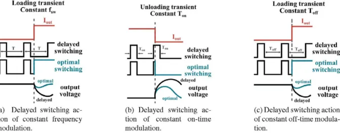
(a) Delayed switching ac-tion of constant frequency modulation.
(b) Delayed switching ac-tion of constant on-time modulation.
output voltage delayed
(c) Delayed switching action of constant off-time modula-tion.
Figure 3: Conceptual scheme of the delayed switching actions of different modulation techniques and comparison with the optimal switching action.
By analyzing the topology and equation (1), it is well-known [11]–[12] that the deviation of the output voltage under unloading transients is greater than under loading transients for Buck converters operating with a small duty cycle.
But these equations are derived assuming that the control is able to react instantaneously after the load transient. However, if constant on-time, constant off-time or constant switching frequency modulations are used, then, there are intrinsic delays that limit the effectiveness of the control. This is because there is an additional voltage deviation that is independent on how fast the control is.
Fig.3 illustrates these delays and compares the response of the modulation with the optimal response:
• In the case of constant frequency modulation (fig. 3a), this would be the case if a positive load step occurs during the off-state begins, as the control is not able to react until the end of the period. In order to overcome this problem, the clock needs to be synchronized with the load disturbance so that an on-time can occur just after the perturbation.
• In the case of constant Ton modulations (fig. 3b), the control is not able to react until the end of the constant on-time if a negative load step occurs during the on-state. In order to overcome this problem, the generation of the constant on-time needs to be reset so that an off-time can occur just after the perturbation.
• In the case of constant Tof f modulations (fig. 3c), the control is not able to react until the end of the constant off-time if a positive load step occurs during the off-state. In order to overcome this problem, the generation of the constant off-time needs to be reset so that an on-time can occur just after the perturbation.
• On the other hand, it is important to point out that ideal hysteretic modulations, which modulate with variable switching frequency, do not exhibit this problem as these modulations do not have time restrictions.
Without considering the ESR and the ESL of the output capacitor, the additional drop of the output voltage due to a time delay is:
AVdelay — ( 2m\ •1 / 1 2 td Aiitd + Ai0td (2)
where td is the time delay, A/¿ is the ripple of the inductor current in steady-state.
In constant frequency and constant off-time modulations, the worst-case is if the control is unable to respond during the whole off-time. Then, td = T0ff = (1 - d)T and the additional drop of the output
voltage is:
A 1/1 All 2 2 1 A / 1) A \ 1 A
AVdelay = ~ — ( ( 1 - d) T A m 1 - a r + A /0( 1 - d)T ) = — A /0( 1 - d)T (3)
Table I: Minimum voltage deviation for a loading transient, Av^ ¡oaí¡ing
for different modulations. The equations do not consider the ESR of the output capacitor.
mn , and an unloading transient, Av™m unloading
Modulation A y i n i n
o loading
A v m i n o unloading
Constant switching frequency (PWM) 1
C Ai0{1
-d)T-\-Ai2
2(Vin - V0)
L — · ——L 1 A2 C 2v0
Constant on-time (COT) 1 Ai2
C 2(Vin - v0)
L 1
C Ai0dT +
Af
2v0
o L
Constant off-time 1
C
Ai2 A- C T i ^l°
¿\i0{1 - d)l-\— L
2(V-V„)
1 Ai20j
· L
C 2v0
Hysteretic / Without delay 1 Alg
c 2(y¿n- L
1 A2
— · ——L C 2v
In constant on-time modulation, the worst-case is if the control is unable to respond during the whole on-time. Then, td = Ton = dT and the additional drop of the output voltage is:
1 / 1 Ail 2 2
A\delay = 7 "T^T" T
C 2 dl
Ai^dT + Ai0dT Ai0dT (4)
Notice that, in both cases, the worst-case additional drop of the output voltage due to the delay does not depend on the inductor of the power stage.
Table I shows the minimum voltage deviation for a loading transient and an unloading transient for different modulations taking into account the additional voltage drop due to the delay of the modulations.
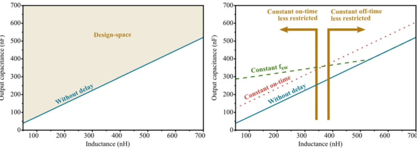
Now, by studying table I, for small duty cycles and constant frequency modulation, the worst-case de-viation of the output voltage could occur under the loading transient. In order to better study how the delays can affect the size of the output capacitor, figures 4 and 5 show the design space for the sizing of the inductor and the output capacitor. The parameters of the converter are fsw = 10MHz, V¿n = 5V,
Vout = 1.2V, iout = 0A 1A, L = 100nH. The maximum allowed static ripple of the output voltage is
vout ± 30mV and the maximum allowed voltage deviation during a transient is vout ± 100mV.: .
• Figure 4a shows the design space for a switching frequency of 10 MHz and supposing that the
modulation does not have a delay in the response. The upper orange area represents the L-C combination that can be designed in order to comply with the dynamic requirements for a load transient.
• Figure 4b shows the same graphic but superposing the design space for constant switching
fre-quency and constant on-time modulations. Several important conclusions can be drawn from this figure:
- By examining the design space for constant switching frequency modulation (green dotted line), notice that above 500nH of inductance, the design space matches the one for the mod-ulation without delay. This is because, below L = 500nH, the worst-case voltage deviation is the loading transient (which exhibits the delay) and , above L = 500nH, the worst-case volt-age deviation is the unloading transient. Therefore, the delay of constant switching frequency modulation does not affect the worst-case voltage deviation in the case of larger values of in-ductance.
- On the other hand, the design space of the constant on-time is parallel to the one of the modulation without delay. This is because the additional voltage deviation caused by the delay adds up to the already larger voltage deviation which is the unloading transient in the case of applications of small duty cycle. Consequently, as opposed to constant switching frequency modulations, the delay of constant on-time modulation always increases the worst-case voltage deviation for these applications.
- Lastly, notice also that around L = 400nH, the design spaces of the constant switching fre-quency and constant on-time modulations intersect. As a result, lower values of the induc-tance benefit constant on-time while greater values of inducinduc-tance benefit constant switching frequency.
• Figures 5a and 5b show the design space of different modulations for switching frequencies of
(a) Design space for a switching frequency of 10 MHz (b) Design space for a switching frequency of 10 MHz and a modulation without delay. and for different modulations.
Figure 4: Conceptual scheme of the delayed switching actions of different modulation techniques and comparison with the optimal switching action for 10MHz.
(a) Design space for a switching frequency of 5 MHz (b) Design space for a switching frequency of 20 MHz and for different modulations. and for different modulations.
Figure 5: Conceptual scheme of the delayed switching actions of different modulation techniques and comparison with the optimal switching action for 5MHz and 20MHz.
eases the delay of these modulations and, therefore, increases the minimum required output capac-itor. Furthermore, by comparing the design spaces of constant switching frequency and constant on-time modulations, it is concluded that constant on-time can be preferable for lower switching frequencies because it exhibits less voltage deviation while constant switching frequency can be preferable for higher switching frequencies.
Clock Pulse Synchronization based on the capacitor current (CPSI
c)
[6] proposes a novel technique called Clock Pulse Synchronization” based on the capacitor current (CPSIc) that significantly reduces the delay in constant switching frequency modulation. Figure 6 shows the proposed technique applied to a V2IC control.
The proposed technique predicts sudden change in the load current by means of monitoring the capacitor current (figure 6a) or the derivative of the capacitor current (figure 6b). When, a positive step occurs, the change is seen on the capacitor current and the oscillator is forced to be synchronized. In this way, an on-time is allowed to occur even if the controller has not end the period set by the clock.
(a) Using the capacitor current (b) Using the derivative of the capacitor current
Figure 6: Proposed Clock Pulse Synchronization technique (in red) on a V2Ic control.
(a) Loading transient response without including CPSIc (b) Loading transient response including CPSIc in the in the control. control.
Figure 7: Loading transient response of the same converter modulated with constant switching frequency without including (a) and including CPSIc (b).
4.4mD., ESL = 650pH, K¿ = 0.13Í1, Kv = 1, Vfamp = 0.6V, Hv(s) = 38400/*. The control is designed
for an inductance of L = 1.3/JH. When the loading occurs at the off-time, the control cannot react till the end of the period and, consequently, the drop of the output voltage is very large (Avout = 350mV).
Fig.7.b shows the very same control and the same loading transient response but including the proposed CPSIc. When the loading occurs, the current through the output capacitor instantly drops which triggers a pulse that resets the clock of the control and the next on-time begins right after the load transient. In the figure, Vth¿ is the threshold voltage of the measurement of the current through the output capacitor
to trigger the clock synchronization. With CPSIc, the control is able to react without delay and the drop of the output voltage is dramatically reduced (98% of reduction). Notice that CPSIc only changes during one period the switching frequency. When the clock is synchronized, the converter returns to switch at the nominal frequency.
(a) Without including CPSIc, the minimum required (b) Including CPSIc, the minimum required output
ca-output capacitance is 11/uF (highlighted in black). pacitance is 700nF (highlighted in black). The re-The response including CPSIc and C=700nF is in the sponse without including CPSIc and C=1. 1/nF is in the
background in grey. background in grey.
Figure 8: Comparison of the minimum required output capacitance to comply with requirements without including and including CPSIc. The load steps are from full load (1 A) to no load (0 A) and vice versa.
• the capacitance of the output capacitor affects the same way to the contributions of both deviations of the output voltage: due to the load disturbance and the additional drop due to the delay i n the response.
• the lower the inductance, the lower the voltage deviation due to load disturbances. But the ad-ditional voltage drop due to the delay i n the response remains the same independently of the inductance.
Therefore, converters w i t h l o w inductance are greater benefited f r o m using CPSIc because, for these
cases, the additional drop of the output voltage due to the delay is dominant. This is very interesting for the case of high-frequency integrated converters. These converters have a low inductance for integration purposes. Fig.8 shows a comparison of the m i n i m u m required output capacitor needed to comply w i t h the requirements of a specific high-frequency converter. The parameters of the converter are the same as i n figures 4 and 5. Fig.8a shows the unloading and the loading transient of V2IC control without including
CPSIc. When C = 1.1/uF, the output voltage just reaches the lower dynamic l i m i t under the loading, so
this is the m i n i m u m required output capacitance. Fig.8b shows the unloading and the loading transient of
V2Ic control including CPSIc. Now, when C = 700nF, the output voltage just reaches the upper dynamic
l i m i t under the unloading. This means that, when CPSIc is included i n the control, the required output
capacitance can be reduced by a 36%, i n this specific example.
Experimental validation
This section documents the experimental validation of CPSIc on a 300kHz Buck converter w i t h V2IC
control. The nominal parameters of the Buck converter are the same as i n figure 7. The P W M controller UC3823 [13] is used to modulate the V2IC control w i t h constant frequency. This P W M controller allows
the external synchronization of the clock signal.
Fig.9 shows the experimental validation of CPSIc. When a positive load step f r o m 0 A to 4 A occurs i n
the off-time, the drop of the output voltage is 340mV (fig.9.a). When the same load transient occurs at the same instant of the off-time but including CPSIc, the drop of the output voltage is 140mV (fig.9.b),
achieving a 58% reduction. Notice that the measurement of the current through the output capacitor (in light blue i n fig.9.b) is inverted as the implemented current sensor inverts the measurement. Notice that the reduction of the drop of the output voltage is not as dramatic as previously shown i n simulations. This is because there is still a certain delay i n the response due to the implementation of CPSIc w i t h discrete
components. For example, notice that there is some delay between the pulse that synchronizes the clock and the actual synchronization of the clock. This delay would be reduced i f CPSIc is integrated i n the
(a) Load step 0A to 4A without including CPSIc in the (b) Load step 0A to 4A including CPSIc in the control. control.
Figure 9: Experimental validation of CPSIc on a 300kHz Buck converter with V2Ic control. Output voltage in green, output current in blue, measurement of the current through the output capacitor in light blue, comparator signal in purple, synchronization pulse (lower digital signal) and duty cycle (upper digital signal) in black.
Summary and conclusions
This paper has presented a throughout analysis of the effect that delays of constant frequency and constant on-time modulations have on the minimum required size of the output capacitor. The analysis can help designers to better understand the most appropriate modulator for their specific application. For example, it has been explained that the delay of constant frequency modulation increases the voltage deviation under a loading transient whereas the constant on-time modulation increases the voltage deviation under an unloading transient. As in small duty cycle applications, the worst-case transient is the unloading, the delay of constant frequency modulation may not affect at all the minimum required output capacitance. On the other hand, the delay of the constant on-time always increases the required capacitance for these applications.
The paper has also shown and validated a technique to improve the dynamic response of controls with constant frequency modulation that is extensible to other modulations and can be implemented in a wide variety of controllers. By using the proposed technique, the delay of constant frequency modulation can be mitigated enough so that it does not affect the minimum required size of the output capacitor.
References
[1] “D-CAPTM mode with all-ceramic output capacitor application,” Tech. Rep. [Online]. Available:
http://www.ti.com/lit/an/slva453/slva453.pdf
[2] “FAN2365. TinyBuckTM 15 a integrated synchronous buck regulator,” Tech. Rep. [Online]. Available: http://www.fairchildsemi.com/ds/FA/FAN2365.pdf
[3] Y. Yan, F. Lee, and P. Mattavelli, “Comparison of small signal characteristics in current mode con-trol schemes for point-of-load buck converter applications,” Power Electronics, IEEE Transactions on, vol. 28, no. 7, pp. 3405–3414, 2013.
[4] “TPS62122. 15V, 75mA high efficienct buck converter.” Tech. Rep. [Online]. Available:
http://www.ti.com/lit/ds/symlink/tps62122.pdf
[5] “LX7167. 3MHz, 2.4A step down converter,” Tech. Rep. [Online]. Available:
http://www.microsemi.com/document-portal/doc download/132564-lx7167-datasheet
[6] J. Cortes, V. Svikovic, P. Alou, J. Oliver, and J. Cobos, “Improved transient response of controllers by synchronizing the modulator with the load step: application to V2Ic,” IEEE Transactions on Power Electronics, vol. Early Access Online, 2014.
[8] J. Cortes, V. Svikovic, P. Alou, J. A. Oliver, and J. A. Cobos, “Comparison of the behavior of voltage mode, v2 and v2ic control of a buck converter for a very fast and robust dynamic response,” in Applied Power Electronics Conference and Exposition, 2014. APEC 2014, 2014, pp. 2888–2894.
[9] ——, “Impact of the control on the size of the output capacitor in the integration of buck con-verters,” in 8th International Conference on Integrated Power Electronics Systems, Feb. 2014, pp. 1–6.
[10] S. Huerta, P. Alou, J. Oliver, O. Garcia, J. Cobos, and A. Abou-Alfotouh, “Design methodology of a non-invasive sensor to measure the current of the output capacitor for a very fast non-linear control,” in Applied Power Electronics Conference and Exposition, 2009. APEC 2009. Twenty-Fourth Annual IEEE, 2009, pp. 806–811.
[11] E. Meyer, Z. Zhang, and Y.-F. Liu, “An optimal control method for buck convertersusing a practical capacitor chargebalance technique,” Power Electronics, IEEE Transactions on, vol. 23, no. 4, pp. 1802–1812, 2008.
[12] ——, “Controlled auxiliary circuit to improve the unloading transient response of buck converters,” Power Electronics, IEEE Transactions on, vol. 25, no. 4, pp. 806–819, 2010.