An analysis of the surface-normal coupling efficiency of a metal grating
coupler embedded in a Scotch tape optical waveguide
Carlos Ángulo Barrios , Víctor Canalejas-Tejero
A B S T R A C T
The coupling efficiency at normal incidence of recently demonstrated aluminum grating couplers in-tegrated in flexible Scotch tape waveguides has been analyzed theoretically and experimentally. Finite difference time domain (FDTD) and rigorously coupled wave analysis (RCWA) methods have been used to optimize the dimensions (duty cycle and metal thickness) of Scotch tape-embedded ID Al gratings for maximum coupling at 635 nm wavelength. Good dimension and tape refractive index tolerances are predicted. FDTD simulations reveal the incident beam width and impinging position (alignment) values that avoid rediffraction and thus maximize the coupling efficiency. A ID Al diffraction grating integrated into a Scotch tape optical waveguide has been fabricated and characterized. The fabrication process, based on pattern transfer, has been optimized to allow complete Al grating transfer onto the Scotch tape waveguide. A maximum coupling efficiency of 20% for TM-polarized normal incidence has been mea-sured, which is in good agreement with the theoretical predictions. The measured coupling efficiency is further increased up to 28% for TM polarization under oblique incidence. Temperature dependence measurements have been also achieved and related to the simulations results and fabrication procedure.
1. Introduction
Implementation of photonic and optoelectronic devices and systems on flexible supports is a subject of increasing interest because it opens the door to new device functionalities as com-pared to conventional schemes on rigid substrates. For example, flexible films can be wrapped around curved and angled surfaces enabling conformal integration of photonic sensors and electronics on hemispherical lenses [1] and human body parts [2]. These technologies can also produce tunable optical devices for adaptive photonic systems [3] and flexible waveguides for interconnections
[4-6]. This has boosted research and development of innovative optical materials and nanofabrication methods targeting simpli-city, low cost, high-throughput and mass production.
Polymeric materials have been traditionally used to implement flexible optical configurations as they can be customly synthesized to offer targeted optical, mechanical and thermal characteristics. This can be done by properly engineering the chemical composi-tion, doping (e.g. with dyes or nanoparticles) and synthesis
conditions of the polymers. In addition, inorganic materials, like chalcogenide glass [7] and Si [8], can be incorporated by well-known techniques such as low-temperature deposition and pat-tern transfer onto polymeric substrates to provide specific optical functionalities (e.g. high-index-contrast and non-linear features).
Conventional pressure-sensitive adhesive (PSA) polymeric tapes, such as Scotch office tapes, are flexible, can be adhered to a variety of surfaces by applying slight pressure without the need for solvent, heat, UV or water for activation. They can also be made highly transparent at optical wavelengths, like general purpose office tapes made of polypropylene films. These characteristics make PSA polymeric tapes suitable material platforms to develop cost-effective and easy-to-use flexible and sticky optical wave-guides. To couple light into a PSA tape, out-of-plane (normal) optical coupling appears to be an appropriate procedure due to the quasi-2D geometry of tapes and the difficulty in achieving po-lished facets for direct in-plane optical coupling. In this respect, diffraction gratings are well-suited configurations [9], particularly when relatively large spot beams are to be coupled, a planar coupling structure is required, and the application is not critically power limited.
Al diffractive grating couplers. The latter consisted of 2D nanohole arrays (NHAs) drilled in an Al thin film incorporated to the PSA tape by using a simple stick-and-peel transfer procedure [11 ]. Due to the NHA 2D geometry (square lattice), light incident onto the grating coupler was split into four normal propagation directions in the tape waveguide, resulting in a low one-direction coupling efficiency (3.6%). For most applications, maximum coupling into a given direction is desirable, for which a ID (stripe array) grating coupler is advantageous over a 2D configuration. In this work we address this issue by analyzing the surface-normal coupling effi-ciency of a 1D Al grating coupler embedded in a Scotch tape wa-veguide. The analysis is focused on normal incidence in order to evaluate the capability of the coupler to be directly adhered onto the flat active surface of semiconductor light sources (light emit-ting and laser diodes) and photodetectors. The coupling graemit-ting is modeled through computer simulations to determine the optimal dimensions (duty cycle, metal thickness and grating length), sen-sitivity to the tape refractive index, and best incident beam para-meters that maximize the surface-normal coupling efficiency. Based on the theoretical analysis, an actual device that increases significantly the aforementioned reported one-directional cou-pling efficiency is demonstrated, and both, its temperature de-pendence and angular response are measured.
2. Device fabrication
2.2. Aluminum ID grating fabrication
Al ID gratings were first fabricated on a 1 cm x 1 cm poly-carbonate (PC) substrate from a standard compact disc (MPO Ibérica, Madrid, Spain) as follows [12]. The PC chip was washed with detergent in ultrasonic bath, rinsed in deionized water (DIW) and isopropyl alcohol and dried with N2 flow. Then, an e-beam
evaporated 100-nm-thick layer of Al was deposited on the flat surface (i.e., with no track) of the PC substrate. Next, ZEP-520 positive tone e-beam lithography (EBL) resist was spin-coated on the Al surface resulting in a 120 nm thick resist film. The chip was then immediately baked for 10 min at 120 °C to remove solvent residues and improve both resist uniformity and resist adhesion to the substrate. Stripe arrays of 500 nm pitch were patterned in the resist film by using a Crestec CABL-9000C high resolution EBL system (acceleration voltage=50 keV, beam current =100 pA, ex-posure time = 100 us). The exposed resist was developed at - 1 5 °C for 10 s and N2-dried. Next, inductively coupled plasma (ICP) chemical dry etching was used to drill lines in the Al layer down to the PC substrate using the patterned ZEP-520 film as a mask. The ICP process was achieved using BC13 (20 seem) and Cl2 (10 seem) gases, and RF and ICP powers of 100 W. Immediately after the ICP etch, the chip was rinsed in DIW for 5 min to dissolve residual A1C13. Then, 02 plasma was used to remove resist residues. Finally, the chip was exposed to an additional 02 plasma treatment to allow subsequent nanostructured Al film delamination.
The latter plasma step was a necessary modification relative to our previous fabrication of releasable NHAs on PC [10,11 ]. The EBL writing time for defining stripes was much longer than that for nanoholes. This over-exposure modified the PC surface, increasing the Al stripe-PC bonding strength and avoiding the complete subsequent detachment of the ID Al gratings by a stick-and-peel procedure. The plasma oxygen treatment solved this problem by slightly etching PC and critically undercutting the Al stripes. The undercut decreases the interfacial area between Al and PC, weakening the bonding force between them. Fig. 1(a) and (b) shows a photograph of two 1.2 mm x 1.2 mm Al ID gratings fabricated on PC and a scanning electron microscope (SEM) top grating image (stripe width ~270nm), respectively.
b)
2.2. Grating-waveguide integration
A general purpose 50-(im-thick transparent Scotch tape (#550 Scotch®, 3M, St. Paul, MN, USA) was stuck on a 1.2 mm x 1.2 mm Al ID grating (period = 500 nm, stripe width=270 nm) on PC, the tape length being perpendicularly oriented with respect to the Al stripe direction. After applying finger pressure at room tempera-ture, the tape was peeled off, resulting in complete Al grating transfer onto the tape thanks to the aforementioned 02 plasma treatment. To facilitate handling, reduce light scattering and avoid dust particle contamination, a bare piece of Scotch tape was stuck on the sticky side of the former with the same orientation, em-bedding the Al grating between two tapes ("double-tape" config-uration) as reported in [10] (Fig. 1(c)). Finally, a 2-mm-wide wa-veguide was created by simply cutting the double-tape with a scalpel (Fig. 1(d)).
matched layer (PML) boundary condition was employed along the incident-beam propagation direction (z-axis) and along the wa-veguide direction (x-axis). Frequency analysis of the coupling ef-ficiency was achieved by launching a pulsed excitation towards the Al grating and calculating the fast Fourier transform (FFT) of the time-domain field components on the waveguide monitor surface. Continuous wave (CW) analysis of the coupling efficiency was carried out by launching a 635-nm-wavelength (operation wavelength) excitation and recording the power flux through the waveguide monitor area. Simulations were achieved for both TE (£-field along y-axis) and TM (£-field along x-axis) incident light polarizations.
4. Results and discussion
4.1. Simulation results
3. Device modeling
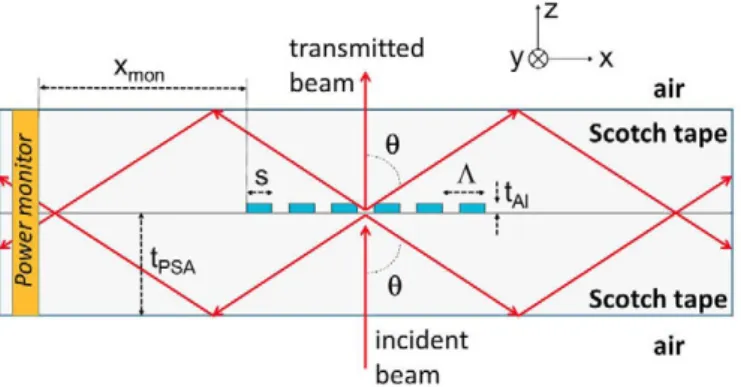
The device performance was computer simulated by using 2D finite difference time domain (FDTD) and rigorously coupled wave analysis (RCWA) methods [13]. Fig. 2 shows a schematic cross-section of the simulated structure. The geometry is invariant along the y-axis. It consists of an Al stripe grating embedded between two 4-(xm-thick PSA tapes in an air background. The thickness of the simulated PSA tape (tPSA) was chosen to be smaller than that of the actual tape (50 urn) in order to reduce both, computation time and computer memory requirements. The grating period is
A = 500 nm. The Al stripes are along the y-axis and all have the
same width (s) and thickness (tA1). The dielectric constant of Al was modeled by the frequency dependent Drude-Lorentz equation according to the material parameters found in [12]. The refractive indexes of the PSA tape (nPSA) and air (nair) were assumed to be frequency-independent and equal to 1.45 (measured with re-flectance interferometry) and 1, respectively.
FDTD method was used to calculate the coupling efficiency (coupled power/incident power) of finite (limited number of per-iods) and semi-infinite length gratings whereas the diffraction efficiency (diffracted power/incident power) of infinite length gratings was analyzed through the RCWA algorithm (number of harmonics=5). All simulations were carried out at normal in-cidence (perpendicular to the grating). The coupling efficiency was computed by launching a Gaussian beam of 1/e width W, and re-cording the normalized power flux through a cross-sectional z-y surface (power monitor) of the double-tape waveguide placed at Xmon (ranging from 9 urn to 15 urn) from the grating edge. Perfectly
tz
s
- S
V
•^mon
transir
s
\ .
'itted
y¿ ^
0
s^
¿* — _ *TA I
8 \ N . /
incident beam
•X
s. Scotch tape
Scotch tape
air
Fig. 2. Schematic cross-sectional diagram of the simulated ID Al grating embedded
between two PSA Scotch tapes of thickness tPSA- The incident beam is diffracted at
an angle 8 by the grating and coupled into the double-tape waveguide. The coupled propagating power is calculated by FDTD computation of the power flux through a cross-sectional surface of the waveguide (power monitor) placed at a distance xmon
from the grating edge.
Under normal incidence, wavelengths (A) coupled to the wa-veguide should meet: i) the diffraction equation: Asm6={mA¡ nPSA), and ii) the total internal reflection (TIR) condition: sine* > nair/nPSA, where 6 is the angle of the diffracted beam and m is an integer. This leads to the following coupling condition:
n3kA<\m\2 < nKAA (1)
For m = l (1st diffraction order), A = 500nm, nPSA=1.45 and na i r= l , Eq. (1) states a coupling bandwidth of [500 nm, 725 nm].
Fig. 3 shows the calculated spectral distribution of the power coupled into a double-tape waveguide embedding a 14-period-long Al grating for TM (red line) and TE (black line)-polarized in-cident light. The Al stripe width and thickness are 250 nm and 100 nm, respectively. It is seen that the coupled power spectra exhibit a bandwidth that approximately coincides with that de-rived from the ray-theory-based Eq. (1) for m = \. Similar band-width was obtained for TE-polarization. The operation wavelength 635 nm lies in the spectral region of maximum coupling. In ad-dition, at this wavelength, the used Scotch tape is highly trans-parent [10], Al absorption loss is relatively low (extinction coefficient=7.3) and there is abundant availability of cost-effective semiconductor optoelectronic devices.
0.30-1
>~ 0.25 <D
O 0.20
CL
"8
0.15
N
ro o.io
O 0.05
o.oo
I ' } ' I • I ' • I ' I
1 1
1 1
i A A '
i fI f 1 /1 /1 A1
i •
i
itm VA \
Í <
\
TE
Jf i l \ >.
i l 1 • 1 1 1 1 r -L- 1 1 1 1
400 500 600 700 800 900
wavelength (nm)
Fig. 3. FDTD-calculated spectra of the normalized power coupled into a waveguide
Fig. 4. RQVA-calculated diffraction efficiency at 635-nm-wavelength of an infinite length ID Al grating of period 500 nm embedded between PSA tapes as a function of the
Al stripe width (s) and thickness (tAi) for TM (a) and TE (b) incident light polarizat
Fringes seen in Fig. 3 are attributed to Fabry-Perot (F-P) re-sonances produced by reflections at the tape/air interfaces and the Al grating. Since the configuration is not lossless, the amplitude of those fringes is greatly reduced for thicker tapes like that of the actual device. In particular, assuming that the F-P resonator finesse
FSK n\{a• tpsA) [14], where a is the resonator overall loss coeffi-cient, the finesse for tPSA=50 urn (experimental device) is that for tP S A=4um divided by 12.5, and the peak (Jmax)-to-valley (/min) intensity ratio would be [14]: Jmax/Jmin=l+(2F/7r)2 = 1.0025.
The diffraction equation indicates that, besides the zero-order (m=0) diffraction beam (i.e. directly transmitted/reflected beam), the analyzed ID Al grating only produces + 1st order diffraction beams (lml = l) in reflection and transmission at 635 nm wave-length, with 0=61.15°. Fig. 4 plots the RCWA-computed total (transmission+reflection) 1st order diffraction efficiency (here-after, diffraction efficiency) at 635 nm wavelength of a ID Al grating embedded in PSA tapes for different values of Al stripe width (s) and thickness (tA1). The maximum efficiencies for TM and TE polarizations are 0.27 (s=250nm, tA1=125nm) and 0.23 (s=250 nm, tAi=175 nm), respectively. For TM, the diffraction efficiency is in the range 0.240.27 for tA[=100150 nm and s = 2 0 0 -300 nm, whereas for TE, the efficiency is within 0.19-0.23 for tA1=100-200 nm and s=250-300 nm. These values indicate good dimension tolerance.
As indicated in the previous section, the refractive index of the tape (nPSA) has been assumed to be uniform and equal to 1.45 according to reflectance interferometry measurements carried out on a piece of tape. This should be considered as an effective index value since the actual tape consists of a polypropylene backing and a synthetic acrylic adhesive material. Since the latter is directly contacting the grating, it is relevant to evaluate the effect of pos-sible deviations of the considered nPSA on the diffraction efficiency. For a grating of dimensions s = 2 5 0 n m and tA1=100nm, it was calculated (Fig. 5) that, for nPSAe[1.40, 1.50], the maximum varia-tions of TM and TE efficiencies relative to the corresponding values for nPSA=1.45 were 1% and 5.5%, respectively, both occurring at nPSA=1.40. These variations are not particularly substantial taking into account the considered large nPSA variations. Note that this analysis not only determines the effect of under- or over-esti-mating the actual tape refractive index, it also reveals that the modeled structure is low-sensitive to moderate (10~4-10~3) re-fractive index changes of the tape, which is an interesting feature for implementing temperature-insensitive optical interconnec-tions to the printed circuit board (PCB) level.
^
o
£=
CD O
a=
CDc O
-4—»
Ü
03
H=
I D
CD
>
•4—' CO CD
f
O
CD
m
>
-4i2 -6
n • r n • 1~
TM
TE
— i ' 1 ' 1 ' 1 ' 1 ' 1 —
1.40 1.42 1.44 1.46 1.48 1.50
nPSA
Fig. 5. Variation of the diffraction coupling efficiency relative to that for nPSA= 1-45 as a function of the tape refractive index in the interval [1.40,1.50], for TM (black square dots) and TE (red circular dots) polarizations. The grating geometry is s=250nm and tAi = 100nm. (For interpretation of the references to color in this figure legend, the reader is referred to the web version of this article.)
In our model, it has been also assumed that the adhesive ma-terial fills the grating trenches uniform and conformally, which is a reasonable assumption due to the good wetting capability of syn-thetic acrylic adhesives. However, it is conceivable the existence of air voids between the Al stripes and therefore pertinent to analyze its effect on the grating efficiency. This was achieved by calculating the TM and TE coupling efficiencies of an embedded grating (s=250 nm, tAi=100 nm) with tArthick air regions between the Al stripes. The efficiency variations (efficiency with voids - efficiency without voids) relative to that to the case of no voids were - 8.65% and 14.95% for TM and TE, respectively. Although these are sig-nificant variations, particularly for TE polarization, it should be noted that the modeled void-containing case is an extreme situa-tion where all trenches are empty (filled with air). In the actual device this is expected to be unlikely because the adhesive material is soft enough to flow under the applied pressure and dwell-time conditions. Hereafter, all simulation results will correspond to the model geometry and parameters described in Section 3, that is, with tape material of nPSA= 1.45 that fills all grating trenches.
rediffraction transmission
1 o
H,
-1.0
Fig. 6. Hy-field distribution in a semi-infinite ID Al grating (red line) embedded
between two PSA tapes for a TM- polarized, 635-nm-wavelength, 5-nm-wide Gaussian beam impinging the grating at x—17.5 nm. L is the minimum distance for a diffracted ray to bounce twice in the grating. Rediffraction occurs because x > L ( = 14.4 nm); the resulting rediffracted beams are normal to the grating and, therefore, not coupled into the waveguide. (For interpretation of the references to color in this figure legend, the reader is referred to the web version of this article.)
should be taken into account when analyzing the grating coupling efficiency. Rediffraction occurs when a diffracted beam is reflected at a waveguide/air interface and the reflected beam impinges the grating [15]. The rediffracted beam does not meet the total internal reflection condition and therefore reduces the power coupled into the waveguide, i.e. the coupling efficiency. The minimum distance for a diffracted ray to bounce twice in the grating will be referred to as the rediffraction length I, and is given by:
L = (2tPSA)tani? (2)
From a simple ray theory perspective, rediffraction takes place for incident beams wider than L and/or for incident beams hitting the grating at a distance from the grating edge larger than L. Re-diffraction is illustrated in Fig. 6, which shows the FDTD-calculated magnetic Hy-field distribution in an embedded Al grating when a TM-polarized 5-(im-wide incident beam hits the grating at x = 17.5 urn >L ( = 14.4 urn) and rediffracted beams propagate perpendicularly to the grating reducing the coupling power.
Fig. 7(a) shows the calculated coupling efficiency as a function of the W/L ratio, where W is the 1/e width of a TM-polarized in-cident Gaussian beam measured from the grating (s=250nm, tA1=100 nm) edge. It is seen that the coupling efficiency equals the diffraction efficiency for W/L < 1 and decays for W/L > 1, which is in agreement with the previous ray theory reasoning. A similar behavior is observed in Fig. 7(b) which plots the coupling effi-ciency as a function of the incidence position (x) of a TM-polarized Gaussian beam of 1/e width W=5 urn. These results indicate that, in order to obtain the highest coupling efficiency, the maximum practical length of the grating is L. For longer gratings both, the spot size and position (alignment) of the incident beam on the Al grating should be properly optimized in order to avoid rediffraction.
4.2. Experimental results
A linearly polarized 635 nm wavelength laser diode (World Star Tech TECRL-635) was used to characterize waveguide loss, cou-pling efficiency, beam alignment and incidence angle tolerance. Polarization state of the beam incident on the grating was selected by employing a half-wave plate and a polarizer. A 20 x microscope objective was used to focus the laser beam onto the embedded Al
a)
0.0 0.5 1.0 1.5 2.0 2.5 3.0 3.5W/L
0 . 2 4
C 0.21 -(D O | 0 . 1 8
-O) — 0 . 1 5
-CL
3 '
Ü 0 . 1 2-0 -09
• I • ! ' I
• • • Bv
*
' I ' 1 ' 1
v
,
r
•
I
r
y
y
i • i *
•
i •
^
-0.0 1.8 3.6 5.4 7.3 9.1 10.9 12.7
W / tP S A
b)
0 0x/L
0.5 1.0 1.5 2.0 25
0.25-C 0.20 0)
' o
0)
0.15-c
g- 0.10
o
o
0.05 -I
~i • r
-oo
1 8 3 6 5 4 7 3 9 1X/t, PSA
Fig. 7. Calculated TM coupling efficiency at 635 nm wavelength of a semi-infinite
Al grating (s—250 nm, tAi = 100nm) embedded in PSA tapes as a function of (a) the
incident Gaussian beam width (W) and (b) the incidence position from the grating edge (x) of a 10A-wide Gaussian beam. L is the rediffraction length, i.e., the mini-mum distance for a diffracted ray to bounce twice in the grating and tPSA is the tape
thickness.
gratings to a spot size of approximately 200 urn. Unless stated otherwise, incident light was normal to the grating. Power exiting the double-tape waveguide was measured with a large area (1 cm x 1 cm) photodetector (Newport 818-ST2/DB) placed in close proximity and normally to the waveguide tip; a rectangular aperture of the same dimensions as the tip cross-section (2 mm x 100 urn) in front of the photodetector was used as an spatial filter to suppress the detection of unguided light. This large area photodetector was also employed to record the power im-pinging onto the grating, i.e., light power exiting the objective. Waveguide losses were evaluated by using the cut-back method. The coupled power was also measured as a function of the em-bedded grating temperature by attaching it onto a temperature-controlled holder consisting of a Peltier element and a thermistor. The angular variation of the coupling efficiency was measured by placing the device in a rotation stage with a resolution of +1°.
4.2.2. Waveguide losses and coupling efficiency
a.
c
3 2
o 2 . 8
2 . 4
-^
2 . 0
-1 1
K \
w
\
• i
Ü.
1 • 1 • 1
• T M
• TE
X
N~ \ ]
\ N
.
r 1 1
i ' i • i *
35 40 45 50 55 60
Length (mm)
Fig. 8. Measured output power (Pout) from a double-tape Scotch waveguide for different waveguide lengths for TM (square dots) and TE (circular dots) polariza-tions. Black and red dashed lines are linear fits of the measured data for TM and TE, respectively. (For interpretation of the references to color in this figure legend, the reader is referred to the web version of this article.)
Al grating coupler as a function of the waveguide length for TM (square dots) and TE (circular dots) polarizations of the incident beams. Linear fitting of the measured data indicates waveguide losses of (0.072 + 0.005) m i r r1 and (0.071 + 0.005) m i r r1 for TM and TE polarizations, respectively. These values agree well with the material losses of the Scotch tape determined in our previous work
[10], indicating that waveguide losses are mainly due to material loss and the scattering contribution (due to, e.g., embedded con-taminant particles and/or air bubbles produced during the grating embedment between the tapes) is low.
The coupling efficiency was determined taking into account the measured waveguide losses. The maximum coupling efficiencies for TM- and TE-polarized incident beam were 0.20 and 0.15, re-spectively. These values are smaller than the calculated diffraction efficiencies for s=270nm, that is, 0.25 and 0.22 for TM and TE polarization, respectively. This is attributed to: i) structural im-perfections of the device due to the existence of Al film cracks created during the hand-made transfer procedure, and ii) re-diffraction, which may occur because the laser beam spot is slightly larger than the rediffraction length value for tPSA=50 urn (actual PSA tape thickness): 1=181.5 urn. The presence of Al film cracks introduce undesired light scattering that reduce the overall diffraction efficiency. This problem can be mitigated by (semi-) automating the peeling-off process via an ad hoc electro-me-chanical instrument for optimizing and controlling the peeling angle and speed in order to minimize Al film defects during the transfer operation. The reduction of the coupling efficiency due to the large beam width (W/L>1) was discussed in the previous section (Fig. 7(a)). Smaller incident spot sizes should be obtained through the use of proper focusing optics.
Fig. 9(a) shows Pout as a function of the beam x-position. It is seen that the maximum coupling occurs near the edge (x SK 0.5 urn) of the grating (output waveguide power is measured at x < 0) and decays drastically when the distance of the incident position to the edge is larger than 200 urn. According to the the-oretical analysis of the previous section (Fig. 7(b)), this agrees well with the expected x-position for the coupling power to decrease due to rediffraction (L= 181.5 urn). This effect is clearly observed in
Fig. 9(b), which shows light guiding along the waveguide direction close to the impinging beam position at the edge of the grating coupler. Negligible power propagates along the opposite direction because of light rediffraction at the grating.
a)
1008 0
6 0
4 0
2 0
-0
' ' 777777777
yyyy^T^
'^/////^
y//7/y/^
^v/////^
É1P
\ • • • •
-X (mm)
b)
Fig. 9. (a) Variation of the output power (Pout) from a double-tape Scotch wave-guide with incident TM-polarized beam x-position. Pout error bars are equal or
smaller than the dot size. Output light is collected at x < 0. Dashed region indicates the Al grating extension, (b) Photograph of light guiding along - x-direction when a 635-nm-wavelength laser beam is focused close to the edge of the embedded Al grating (the incident spot is clearly seen). Rediffraction highly attenuates light guiding along the opposite (+x) direction.
CD § O Q . "O
CD O Z! n o CD
>
-*—> CO
CD
Ql
C O
A—>
10
m
>
3 2 1 0 1 2 3 4
-i
•
i
•
•
i
#
•i • i
i i
•
- : i
i • i ' i
•
i
1
i
•
1 I 1
• T E
• T M "
-•
•
i •
i
-i
1 ' 1
20 22 24 26 28 30
Temperature (°C)
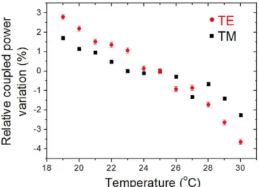
Fig. 10. Variation of the coupled power relative to that at 25 °C as a function of the
temperature for TM (black square dots) and TE (red circular dots) polarizations. (For interpretation of the references to color in this figure legend, the reader is referred to the web version of this article.)
4.2.2. Temperature behavior
(23-27 °C) and, out of this interval, it increases (decreases) as the temperature decreases (increases). The thermo-optic coefficient (TOC) of polymers is on the order of -10~4(°C) _ 1. Thus, the negative value of TOC and the modeling analysis of the coupling efficiency dependence with the tape refractive index (Fig. 5) could explain the measurements trend observed in Fig. 10. However, the experimental relative variations of the coupled power for tem-peratures out of the (23-27 °C) range are approximately two or-ders of magnitude larger than those assuming a tape TOC= - 1 0 ~4 (°C) _ 1. On another hand, thermal expansion of the polymeric PSA tape could originate small variations in the length of the grating period (A) and therefore affect the diffraction effi-ciency. The coefficient of thermal expansion (CTE) for most poly-mers (including polypropylene and acrylic) is on the order of 10~4(oC)~\ Thus, assuming this value for the PSA tape CTE, a temperature variation of 10 °C would result in a period length variation of 0.5 nm. This increment, according to our RCWA cal-culations, would lead to a relative variation of the coupling effi-ciency of approximately 0.1%, which is one order of magnitude smaller than the experimental value. Additionally, the diffraction efficiency variation with A was calculated to be negative for TM polarization (-0.12%/nm) and positive for TE polarization (+0.21%/nm), which does not agree with the measured trends.
Rediffraction could also play a role in the temperature behavior of the device since both, nPSA and A variations modify the dif-fraction angle 6 (difdif-fraction equation) and therefore the re-diffraction length L (Eq. (2)). For example, considering the previous values of TOC and CTE, a temperature increment of 10 °C would result in a I increment of 0.54 um according to the thermo-optic effect, and a L decrement of 0.77 urn according to the thermal expansion effect, for both TM and TE polarizations. If the beam width is larger than these L values (W/L > 1), the diffraction effi-ciency would increase and decrease, respectively (Fig. 7(a)). Therefore, both effects, thermo-optical and thermal expansion, would mostly cancel each other out. Besides, the corresponding variations of the diffraction efficiency obtained from Fig. 7(a) are one order of magnitude smaller than the experimental results.
In view of this, none of the aforementioned material and device parameters appears to be the main cause for the observed tem-perature behavior for temtem-peratures out of (23-27 °C). Thus, the large measured relative efficiency variations might be originated by a more drastic effect like significant grating deformation, which could also alter the angle of incidence and therefore the diffraction efficiency, as will be seen in the next sub-section. Since the tapes embedding the grating were attached manually, it is reasonable to expect that the applied stresses on each of them were not exactly equal at the time of the attachment. This would lead to a differ-ential stress that can be enhanced due to temperature variations and deform the grating, altering its geometry and, therefore, af-fecting the coupling efficiency. It should be mentioned that the measured temperature effect within the studied temperature range was reversible, making the device appropriate for thermo-optic modulation applications. Although further investigations are needed to fully understand the effect of temperature on the optical and mechanical properties of the embedded grating, the tape at-tachment-related stress issue should be taken into account for the development and refinement of future versions.
4.2.3. Non-normal incidence
Despite this analysis is focused on surface-normal coupling, it is convenient from a practical point of view to determine the angular tolerance of the embedded Al grating because of flatness non-uniformities that might be found on both, the emitting/detecting device surface and the coupling element. Fig. 11 shows the mea-sured angular variation of the output (coupling) power for TM and TE polarizations. It is seen that the coupling power for TM
40
20-0
O o
D_ -20
Q_ -40
<
-60
-80
• * • * • * • »
-TE
. . "
V
• - •
'"•
TM
• •
• •
— i — . — i —. — i — i — i —i — i — . —i — . — i — .
-15 -10 -5 0 5 10 15
incidence angle
$
(degree)
Fig. 11. Angular variation of the output power (Pout) relative to that at normal in-cidence (P°out) for TM (black square dots) and TE (red circular dots) polarizations.
AP=P0ut-P°out- Error bars are equal or smaller than the dot size. Collected output
light propagates along the - x-direction. (For interpretation of the references to color in this figure legend, the reader is referred to the web version of this article.)
polarization increases 40% with respect to that at normal incidence when the incidence angle (</>) equals 7°. This means a coupling efficiency of 28%. The TM coupled power at <p=0° varies + 10% for an incident angle variation of + 2° from the normal. Better angular tolerance (lower coupling power variation) around <p=0 is ob-served for TE polarization. A theoretical study of the grating an-gular response is beyond the purpose of this work.
A demonstration of the capability of the fabricated Scotch tape
a)
b)
¿u 0-¡£
-20-^^.
of -
40-- 1 ,
3 o Q_ 6 0
-<
v—'
8 0
1 0 0
-•
i » • ! . *.___»*
• i • "
TE ...•:'! •:-.
« •
* • • *
.-" TM;
' i
•
i
:
•
•
* •
• •-80 -60 -40 -20 20 40 60 80
torsion angle
\\i
(degree)
Fig. 12. Light coupling and guiding in the analyzed flexible waveguiding
config-uration under torsion deformation, (a) Photograph of the operation of the twisted device and sign convention adopted for the torsion angle (v). (b) Measured relative variation of the output power (Pout) for TM (black square dots) and TE (red circular
dots) polarizations. AP—Pouc-P°ouc, where P°out is the output power for the
optical waveguide configuration to work in the case of bending is illustrated in Fig. 12, which shows and characterizes light coupling and guiding under torsion deformation of the flexible device. Longitudinal twisting was carried out by fixing the waveguide exit end and applying a torque to the waveguide end containing the grating coupler via a rotating clamper. It is seen in Fig. 12(b) that acceptable light coupling is obtained for both polarizations even for torsion angles (y/) as large as + 45°.
4.3. Coupling improvement
The measured coupling efficiency is approximately 80% of the theoretical prediction. Thus, although the actual surface-normal coupling efficiency could, in theory, be more increased by a refined and optimized fabrication procedure, no significant enhancement should be expected. Oblique incidence at (p=l° increases the coupling efficiency for TM polarization, as discussed before. However, if the embedded coupler is intended to be attached onto the flat surface of an emitting/detecting semiconductor device, means to provide such an angle, like a plastic or glass wedge be-tween the tape and the emitter/detector surface, should be contemplated.
For further increase in coupling efficiency, different possibilities can be considered, like fabricating a saw tooth shape and adding a metal mirror [16]. However these approaches require a number of extra processing steps, increasing fabrication complexity, and stringent dimension accuracies. In order to maintain the geome-trical and fabrication simplicity of the studied configuration, other materials apart from Al could be examined. For example, the RCWA-calculated surface-normal TM coupling efficiencies at 635 nm wavelength for an embedded grating coupler similar to that studied (s=250 nm, tA1=100 nm A = 500 nm) made of Au, Ag, Cu and crystalline Si (c-Si) were 0.25, 0.29, 0.26 and 0.36, re-spectively. Materials parameters used in the calculations were obtained from the employed simulation software database [13].
That is, as compared to Al, similar efficiencies are predicted for Au and Cu, whereas higher values are obtained for Ag and c-Si be-cause of their lower material absorption at the operation wave-length and, in the case of Si, higher refractive index contrast. Using Ag instead of Al would increase the fabrication cost (Ag is ~425 times more expensive than Al) while offering a quite modest crement in efficiency. On the other hand, Si appears to be an in-teresting alternative to Al as the efficiency increment is more significant and c-Si gratings could be fabricated on silicon-on-in-sulator (SOI) wafers and transferred onto a flexible polymeric film as described in [8]. However, SOI wafers are much more expensive than standard PC compact discs as that used in this work; there-fore, careful evaluation of the performance-cost tradeoff must be carried out for each application.
5. Conclusions
The surface-normal coupling efficiency of a ID Al grating em-bedded in a flexible waveguide made of Scotch tape has been analyzed theoretically and experimentally. Simulations have re-vealed a coupling bandwidth in the visible of ~225 nm for a 500-nm-period grating. A maximum surface-normal coupling effi-ciency of 25 + 2% at 635 nm wavelength for TM-polarized incident beam has been calculated for an Al strip width of 250 + 50 nm and thickness of 125 + 25 nm, indicating good dimension tolerance. The optimal length of the grating is determined by the rediffrac-tion effect, which, in turn, depends on the diffracrediffrac-tion angle and tape thickness. The modeled structure has exhibited low sensi-tivity to variations of the refractive index of the tape, which is desirable for temperature-insensitive (or low sensitive)
applications. An actual device with stripe dimensions within the calculated optimum ranges has displayed a maximum perpendi-cular coupling efficiency of 20% for TM polarization at 635 nm wavelength. This value is significantly larger than that of the first demonstration of this type of optical material platform and close to that of its ideal (simulated) counterpart. Temperature depen-dence measurements have shown larger power coupling varia-tions than should be expected due to the tape TOC and CTE alone, suggesting that other issues such as differential stress between the tapes embedding the grating may play a major role. The measured coupling efficiency is increased up to 28% for oblique incidence
{(p=l°) and TM polarization. Measurements have also indicated a
moderate angular sensitivity around normal incidence for small angle deviations. This study provides useful insight into the de-sign, fabrication and performance of this recently introduced easy-to-fabricate flexible optical component, and the exhibited coupling efficiency is large enough to be used for applications like flexible optical connections and modulators, optical (bio)sensing and mi-cro-opto-electro-mechanical systems (MOEMS) based on cost-ef-fective ready-to-use solutions.
Acknowledgments
This work was funded by Fundación BBVA through "2015 edi-tion of the BBVA Foundaedi-tion Grants for Researchers and Cultural Creators".
References
[1] H.C. Ko, M.P. Stoykovich, J. Song, V. Malyarchuk, W.M. Choi, C. Yu, J.B. Geddes,
J. Xiao, S. Wang, Y. Huang, J.A. Rogers, A hemispherical electronic eye camera based on compressible silicon optoelectronics, Nature 454 (2008) 748.
[2] M.C. McAlpine, H. Ahmad, D. Wang, J.R. Heath, Highly ordered nanowire arrays
on plastic substrates for ultrasensitive flexible chemical sensors, Nat. Mater. 6 (2007) 379.
[3] I.M. Pryce, K. Aydin, YA. Kelaita, R.M. Briggs, H.A. Atwater, Highly strained
compliant optical metamaterials with large frequency tunability, Nano Lett. 10 (2010) 4222.
[4] E. Bosmand, G. Van Steenberge, B. Van Hoe, J. Missinne, J. Vanfleteren, P.
Van Daele, Highly reliable flexible active optical links, IEEE Photon. Technol. Lett. 22 (2010) 287.
[5] R. Brack, P. Muellner, N. Kataeva, A. Koeck, S. Trassl, V. Rinnerbauer,
K. Schmidegg, R. Hainberger, Flexible thin-film polymer waveguides fabricated in an industrial roll-to-roll process, Appl. Opt. 52 (2013) 4510.
[6] L. Li, Y Zou, H. Lin, J. Hu, X. Sun, N.N. Feng, S. Danto, K. Richardson, T. Gu,
M. Haney, A fully-integrated flexible photonic platform for chip-to-chip optical interconnects, J. Lightwave Technol. 31 (2013) 4080.
[7] L. Li, H. Lin, S. Qiao, Y Zou, S. Danto, K. Richardson, J.D. Musgraves, N. Lu, J. Hu,
Integrated flexible chalcogenide glass photonic devices, Nat. Photon. 8 (2014) 643.
[8] Yu Chen, Huan Li, Mo Li, Flexible and tunable silicon photonic circuits on
plastic substrates, Sci. Rep. 2 (622) (2012) 1-6.
[9] M. Neviere, R. Petit, M. Cadihac, About the theory of optical grating
coupler-waveguide systems, Opt. Commun. 8 (1973) 113.
[10] C.A. Barrios, V. Canalejas-Tejero, Light coupling in a Scotch tape waveguide via
an integrated metal diffraction grating, Opt. Lett. 41 (2016) 301.
[11] C.A. Barrios, V. Canalejas-Tejero, Compact discs as versatile cost-effective
substrates for releasable nanopatterned aluminium films, Nanoscale 7 (2014) 3435.
[ 12] C.A. Barrios, V. Canalejas-Tejero, S. Herranz, M.C. Moreno-Bondi, M. Avella-Oliver, R. Puchades, A. Maquieira, Aluminum nanohole arrays fabricated on polycarbonate for compact disc-based label-free optical biosensing, Plas-monics 9 (2014) 645.
[ 13] Rsoft Components Design Suite [software], <https://optics.synopsys.com/rsoft/>.
[14] B.E.A. Saleh, M.C. Teich, Fundamentals of Photonics, 2nd ed., John Wiley &
Sons, Inc., Hoboken, New Jersey 2007, pp. 365-375.
] 15] N. Destouches, D. Blanc, J. Franc, S. Tonchev, N. Hendrickx, P. Van Daele, O. Parriaux, Efficient and tolerant resonant grating coupler for multimode optical interconnections, Opt. Express 15 (2007) 16870.