Enhanced exchange and reduced magnetization of Gd in an Fe/Gd/Fe trilayer
M. Romera,1 M. Muñoz,2 M. Maicas,1 J. M. Michalik,4,5 J. M. de Teresa,3,4,5 C. Magen,3,4,6 and J. L. Prieto1 1 Instituto de Sistemas Optoelectrónicos y Microtecnología, Universidad Politécnica de Madrid, Avenida Complutense s/n,E-28040 Madrid, Spain
2Instituto de Física Aplicada, CSIC, C/Serrano 144, E-28006 Madrid, Spain
3Laboratorio de Microscopías Avanzadas, Instituto de Nanociencia de Aragón, Universidad de Zaragoza, E-50018 Zaragoza, Spain ^Departamento de Física de la Materia Condensada, Universidad de Zaragoza, E-50009 Zaragoza, Spain
^Instituto de Ciencia de Materiales de Aragón, CSIC-Universidad de Zaragoza, E-50009 Zaragoza, Spain 6Fundación ARAID, E-50004 Zaragoza, Spain
The exchange interaction of Gd adjacent to Fe has been characterized by transport measurements on a double spin valve with a Fe/Gd/Fe trilayer as the middle layer. Our measurements show that the ferromagnetism of the Gd is enhanced by the presence of the Fe, and it remains ferromagnetic over its Curie temperature up to a thickness no smaller than 1 nm adjacent to the Fe. This thickness is more than double what has been reported before. Additionally, the saturation magnetization of the thin Gd layer sandwiched in Fe was found to be half of its bulk value. This reduced magnetization does not seem to be related to the proximity of Fe but rather to the incomplete saturation of Gd even for very high fields.
I. INTRODUCTION
Rare earths (REs) and their compounds with transition metals (TMs) are of great importance in modern magnetism, permanent magnets (NdFeB or SmCo) being perhaps the most notorious example. The antiferromagnetic (AF) coupling of many REs with TM1 recently opened the door to very inter-esting science. In giant mangetoresistance (GMR) multilayers, RE and TM coupling can result in an inverse GMR.2 The alloys of RE and TM can also lead to negative mangetoresistance (MR) in a structure, as the alignment of its magnetic moment with the external magnetic field will depend on the proportion of RE and TM. Typical examples for this are the Gdi_xCox and Gdi_x(CoFe)x alloys,3-5 whose magnetic moment and spin polarization can be adjusted with the composition.6 Other recent applications of REs and their alloys are the reduction of spin-transfer noise in reading heads,7 tuning the resonance of a magnetic domain wall,8 and the nucleation and characterization of an in-plane magnetic domain wall.9,10
Any study or application related to thin films of REs and their alloys with TMs requires a careful characterization of their magnetic structure. This is usually done with techniques that are available only in a few sites around the world, such as resonant x-ray magnetic scattering or polarized neutron reflectometry. Transport measurements are more standard tools to determine the direction of magnetization of a structure through its anisotropic magnetoresitance (AMR),11 but they are not sensitive enough to other important effects, such as interface coupling and surface effects.
In this work we characterize the properties of Gd films and their coupling with adjacent Fe layers via transport measure-ments in a double spin valve (DSV). We show that the Gd remains ferromagnetic well above its bulk Curie temperature when it is close to the Fe layer. This enhanced ferromagnetism extends more than 1 nm into the Gd layer, which is more than double the distance reported previously,12 measured by x-ray resonance magnetic reflectivity and magnetic circular dichroism. Also, we show that the magnetization of Gd in thin
films is substantially reduced from the bulk value. The mag-netization we measure in thin films is 1030 emu/cm3, while the bulk value is almost double, 2056 emu/cm3. A 20-30% reduction of the magnetization of Gd in Gd/Fe multilayers has previously been reported by several groups, 13~15 but very rarely
is the reduction as large as the one reported here.16,17 Beyond the different values obtained for the enhanced exchange and the reduced magnetization of Gd, this work shows that a DSV is an efficient tool for characterizing magnetic materials in general and compounds of REs in particular, which is of great interest for many magnetic research fields.
II. EXPERIMENTAL DETAILS
the independent layers and the trilayers of Fe/Gd/Fe for the different thicknesses of Gd were characterized by VSM. All these hysteresis loops allowed us to know the switching sequence for the multilayer stack. The resistance value of this DSV will depend on the relative orientation of the two spin valves CoFe(pinned)/Cu/Fe and Fe/Cu/CoFe(free), as the Gd that separates these two spin valves does not contribute to the MR.18
III. RESULTS AND DISCUSSION
Before analyzing the transport measurements, it is worth noting a few details of the artificial ferrimagnetic trilayer Fe(3)/Gd(í)/Fe(3). Fe and Gd form a very good interface as the solubility of Fe on Gd is very poor19 [see also our
STEM-EELS map in Fig. 1(a)]. At the interface, Fe and Gd couple antiparallel. The length scale of this strong coupling was measured on about 1-2 interatomic distances inside the Gd layer (~0.5 nm) and predicted to hold way over its Curie temperature.12 The magnetization process of a Fe/Gd/Fe
trilayer will depend on the ratio of the magnetic moment of the Fe layers to the magnetic moment of the Gd layer. When (at low temperatures) the magnetic moment of Gd is larger than that of Fe, the Gd aligns with the external field and the Fe is antiparallel (Gd-aligned state). If the external field increases further, the Zeeman energy is too large for the Fe to remain antiparallel, so the magnetization of both layers aligns with the field away from the interface, while the interface aligns in plane but perpendicular to the external field. This configuration is called the twisted state, and it results from minimizing both the Zeeman and the exchange energies.20'21
If the magnetic moment of Fe is larger than that of Gd (high temperatures), the situation is reversed, and the Fe aligns with the field (Fe-aligned state) until the twisted state is reached for larger fields.
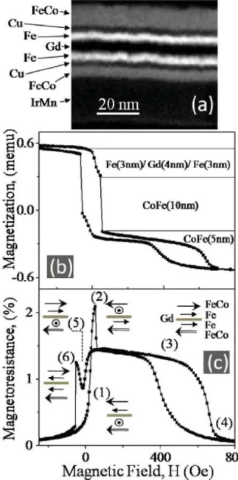
Figure 1(a) shows a map of the integrated intensity of the Fe ¿2,3 edge in a SI obtained in the DSV with 4 nm of Gd (t = 4 nm). As can been seen in this image, the Fe layer introduces a roughness that is transmitted to all the layers above. In all the samples analyzed by STEM-EELS we appreciate the roughness introduced by the Fe layer, and it can be estimated on 0.33 nm rms for the bottom Fe layer and 0.43 nm rms for the top Fe layer, with a length scale of about 9 nm. These values are similar to those reported by other authors.16-17-19
Figures 1(b) and 1(c) show the hysteresis loop and the MR response of this DSV with 4 nm of Gd, measured at 300 K. At this temperature the Gd layer is expected to be paramagnetic
(Tc of Gd in bulk is 293 K). If this is the case, neither Fe layer would be exchange coupled through the Gd, and they would be free to switch independently. Starting from negative fields, as the field is reduced from saturation the bottom Fe layer (the one with less roughness) starts to switch gradually [point (1) in Fig. 1(c)]. The resistance reaches a maximum as the bottom Fe layer switches completely and the top Fe layer is partially switched [point (2)]. Then there is a sharp drop of resistance corresponding to the switching of the free CoFe layer. This sharp transition also "drags" the top Fe layer to complete its switching as it is partially magnetostatically coupled to the CoFe free layer due to its roughness (orange-peel coupling). Finally, the pinned layer switches, and all the layers are parallel
at point (4) in Fig. 1(c). When the loop is plotted from positive to negative fields, the first layer to switch is the pinned FeCo and then the bottom Fe. In this case, though, we measure a drop in the resistance [point (5)] as the bottom spin valve is almost in a parallel state and the top spin valve is in a parallel state. The resistance rises again when the bottom Fe layer completes the switching and the top Fe layer is almost fully switched
[point (6)]. Finally, the free layer completes the switching, again dragging the top Fe layer.
The two asymmetric peaks represented by points (2) and (5) in Fig. 1(c) are a signature of the Gd being paramagnetic and the Fe layers switching independently. If the Gd is removed, leaving a unique layer of Fe in the middle of the DSV, points (2) and (5) in Fig. 1(c) should have similar MR values because the whole Fe layer would switch in a single transition. This is shown in Fig. 2(a) for a room-temperature MR loop of a DSV with only Fe in the interlayer. The MR loops can be described as follows: coining from the DSV saturated at negative fields, the Fe layer is the first to start switching at point (1), increasing slightly the resistance. Before the Fe completes its switching, the free FeCo layer switches, and the DSV reaches the maximum resistance at point (2). Only at slightly higher positive fields does the Fe layer complete its switching, and the resistance drops slightly to the plateau at
Magnetic Field, II (Oe)
-200 O 200 400 600 800 Magnetic Field //(Oe)
FIG. 2. Room-temperature MR curve (a) for a DSV with 0 nm of Gd (i.e., 6 nm of a continuous Fe layer in the middle of the DSV) and (b) for a DSV with 2 nm of Gd. The inset in (b) is a STEM-EELS map at the Fe ¿2,3 edge. The scans of this sample show a Gd thickness between 2.5 and 2.8 nm.
point (3). The Fe and the free FeCo layers are again slightly coupled due to the roughness introduced by the Fe (orange-peel coupling). Finally, the pinned FeCo switches to complete the saturation for positive fields.
Figure 2(b) shows the room-temperature MR response of the DSV with 2 nm of Gd (icd = 2 nm). This sample also shows a symmetrical switching for both branches of the hysteresis loop, indicating that the Fe/Gd/Fe switches all as a single layer. If this is the case, the Fe layers are exchange coupled through the Gd layer, which must be ferromagnetic. The inset in Fig. 2(b) shows a STEM-EELS Fe ¿2,3 integrated intensity map of the DSV edge, showing the continuity of the Gd layer. The intensity line profiles give a thickness of the Gd layer for this sample between 2.5 and 2.8 nm. This entire thickness is kept ferromagnetic at room temperature by its exchange interaction with the adjacent Fe layers. The MR loop shown in
Fig. 2(b) maintains its shape and MR values up to 350 K, the
highest temperature we can measure in our cryostat and well over the Curie temperature of the Gd.
The thickness of Gd where the ferromagnetism is enhanced by the presence of Fe was measured by previous authors12 at
300 K in about 0.4 nm close to the Gd-Fe interface. Our results show that this thickness could be more than double (1-1.2 nm) up to 350 K. The roughness in our samples is comparable to the one reported in Ref. 12, so it cannot be the reason for the larger value we measure. Additionally, our STEM-EELS maps for this sample with iGd = 2 nm show that only a few scattered
pin-holes might be present in the Gd layer, masked by the effect of the finite thickness of the cross-section specimen, so this is also an unlikely cause for the large exchange distance we measure. In order to confirm that our interpretation of the MR loops in terms of the enhanced ferromagnetism of the Gd layer is correct, we have measured the samples with a thicker Gd layer at lower temperatures. Figure 3 shows the MR loop for the sample with iGd = 4 nm measured at 25 K. At low
-2.0-1.5-1.0-0.5 0.0 0.5 1.0 1.5
Magnetic Field H(kOe)
FIG. 3. MR loop for the sample with 4 nm of Gd at 25 K. The shape of this loop is very similar to the one shown in Fig. 2(a) for no Gd, which shows that the two Fe layers are exchange coupled through the Gd. The inset shows a sequence for several temperatures for a low-field zoom of the loop. The vertical scale of the inset is shown on its right.
temperatures the MR values are similar for both branches, as it is the MR loop for the sample without Gd (tGd = 0 nm). At low temperatures, the layer of Gd is ferromagnetic, and the two Fe layers are exchange coupled through the Gd layer, thus being forced to switch together. The inset in Fig. 3 shows a sequence for the transformation of the asymmetric section of the MR loop as the temperature is reduced. At 25 K the section of the loop that goes from negative to positive fields switches more gradually than in the branch that goes from positive to negative fields. The reason for this, as in all the samples shown in this study, is the magnetostatic coupling via interface roughness between the Fe layer (or Fe/Gd/Fe) and the top FeCo free layer. From negative to positive fields, the first layer to switch gradually is the Fe/Gd/Fe trilayer, and it only completes its switching when the free layer switches. On the other branch, from positive to negative directions, the first layer that rotates is the pinned layer and then again the Fe/Gd/Fe layer, increasing slightly the resistance just before the sharp drop caused by the switching of the free FeCo layer.
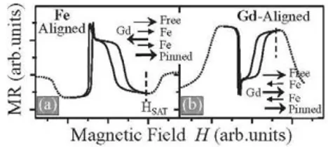
At low temperatures, as we mentioned in the Introduction, the Fe/Gd/Fe can be Gd aligned with the external magnetic field or Fe aligned, depending on which layer has more magnetic moment. The shape of the MR loop for the DSV will depend on whether the Fe/Gd/Fe trilayer is Gd or Fe aligned. Figure 4(a) shows a schematic with the expected shape of the MR loop for an Fe-aligned trilayer, whose shape is similar to the ones shown so far in this work. At the saturation field, the Fe layers are aligned parallel to the free and pinned CoFe
^ •
v i
-tó •
5
-Fe Aligned
_\...._J
„ — > Free
1 G4-»- Fe f
\ \ — • Pinned /
IV
HsAT "Ú
Gd-Aligned
r G dT * F e
" " • Pinned
Magnetic Field H (arb.units)
80
40
3
^ 8 0
-
4
0-tGd=6 nm
^ J
íG¿=10nm EH
\
\¿7*"—_
K2
íG¿=8 nm
A
id
S,
M
-^tGi=\S n m X .
-5 0 5 -5 0 5 Magnetic Field H(KOe)
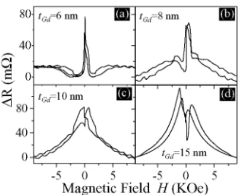
FIG. 5. MR loops measured at 10 K for a DSV with the structure described in Fig. 1 and varying the thickness of the Gd layer, indicated in each plot. The transition from (a) Fe aligned to (d) Gd aligned happens between (b) iod = 8 nm and (c) iod = 10 nm.
layers, giving a minimum of the resistance. For even higher fields, the Fe/Gd/Fe reaches the twisted state20 (represented
by a dotted line in Fig. 4), effectively reducing the thickness of the Fe layer that is aligned with the FeCo layers.
Alternatively, if the trilayer Fe/Gd/Fe is Gd aligned, the shape of the MR loop would be inverted like the schematic shown in Fig. 4(b). Here, as the Gd aligns with the saturating magnetic field, it leaves the Fe antiparallel to the free and pinned CoFe layers, giving the highest resistance value at that field. For even higher fields, the trilayer goes into the twisted state (represented by a dotted line), and the resistance drops again because the Fe begins to rotate toward the field.
We have measured the MR loops for several samples with different thicknesses of Gd in order to find the critical Gd thickness that makes the sample go from Fe aligned to Gd aligned. Figure 5 shows the MR loops measured at 10 K for samples with different thicknesses of Gd. For iGd = 6 nm the
sample is clearly Fe aligned, and for iGd = 15nm it is Gd
aligned. The transition happens between iGd = 8nm and tGd = 10 nm, as can be seen in Figs. 5(b) and 5(c), where the shape of the curve changes.
Selecting iGd = 9 nm as the critical thickness, we can use this
value to estimate the saturation magnetization of the Gd in our thin films. The saturation magnetization of the Fe layerremains roughly constant from 10 K to room temperature for Ms(Fe) =
1545 emu/cm3 (the value for our samples; see Fig. 6); therefore
9 nm of Gd compensating 6 nm of Fe results in a saturation
- 6 - 4 - 2 0 2 4 6
Applied Magnetic Field H (T)
FIG. 6. Hysteresis loop with the field applied perpendicular to the sample plane for a thin film of Ta(3 nm)/Fe(6 nm)/Ta(3 nm) (circles) and a thin film of Ta(3 nm)/Gd(4 nm)/Ta(3 nm) (triangles), measured at 10 K.
magnetization for Gd of Ms (Gd) = 1030 emu/cm3. This value
is considerably smaller than the bulk saturation magnetization for Gd, 2056 emu/cm3, but it is similar to the reduced
magnetization in thin-film Gd reported by other authors.16'17
The saturation magnetization of a single Gd thin film was measured very close to the bulk value (see Fig. 6). This saturation is obtained for an external field of about 3 T, while only half of the moment of the sample follows the external field at 0.5 T. This indicates that this reduced magnetization might not be intrinsically associated with the proximity of the Fe layer, but rather with the formation of perpendicular-to-plane domains.22
In conclusion, we have used a DSV to determine the properties of Gd in a thin film. We find that the Gd remains ferromagnetic well over its Curie temperature for a thickness of more than 1 nm when it is adjacent to an Fe layer. This value is almost double the values reported previously. Additionally, we have measured a reduced magnetization of Gd in thin films, in agreement with previous results. Nevertheless, this reduction seems to be caused by partial magnetization of the Gd film, rather than by the presence of Fe.
ACKNOWLEDGMENTS
This work was partially supported by Project Nos. MAT2008-02770/NAN and MAT2009-08771 from the Span-ish Ministerio de Ciencia e Innovación. M. Romera was funded through the FPU Fellowship No. AP2007-00464.
!R. E. Camley and R. L. Stamps, J. Phys. Condens. Matter 5, 3727 (1993).
2F. E. Stanlet, M. Perez, C. H. Marrows, S. Landridge, and B. J. Hickey, Europhys. Lett. 49, 528 (2000).
3D. Z. Yang, B. You, X. X. Zhang, T R. Gao, S. M. Zhou, and J. Du,
Phys. Rev. B 74, 024411 (2006).
4C. Bellouard, H. D. Rapp, B. George, S. Mangin, G. Marchal, and J. C. Ousset, Phys. Rev. B 53, 5082 (1996).
5X. J. Bai, J. Du, J. Zhang, B. You, L. Sun, W. Zhang, X. S. Wu, S. L. Tang, A. Hu, H. N. Hu, and S. M. Zhou, J. Appl. Phys. 103, 07F305 (2008).
6C. Kaiser, A. F Panchula, and S. S. P. Parkin, Phys. Rev. Lett. 95, 047202 (2005).
7S. Maat, N. Smitch, M. J. Carey, and J. R. Childress, Appl. Phys. Lett. 93, 103506 (2008).
8S. Lepadatu, J. S. Claydon, D. Ciudad, C. J. Kinane, S. Langridge, S. S. Dhesi, and C. H. Marrows, Appl. Phys. Lett. 97, 072507 (2010).
9S. Mangin, G. Marchal, C. Bellouard, W. Wernsdorfer, and B. Barbara, Phys. Rev. B 58, 2748 (1998).
"M. Vaezzadeh, B. George, and G. Marchal, Phys. Rev. B 50, 6113 (1994).
12D. Haskel, G. Srajer, J. C. Lang, J. Pollmann, C. S. Nelson, J. S. Jiang, and S. D. Bader, Phys. Rev. Lett. 87, 207201 (2001).
13M. Sajieddine, Ph. Bauer, K. Cherifl, C. Dufour, G. Marchal, and R. E. Camley, Phys. Rev. B 49, 8815 (1994).
14W. Hahn, M. Loewenhoupt, Y. Y. Huang, G. P. Felcher, and S. S. P. Parkin, Phys. Rev. B 52, 16041 (1995).
15C. Dufour, Ph. Bauer, M. Sajieddine, K. Cherifl, G. Marchal, Ph. Mangin, and R. E. Camley, J. Magn. Magn. Mater. 121, 300 (1993).
16N. Ishimatsu, H. Hashizume, S. Hamada, N. Hosoito, C. S. Nelson, C. T. Venkataraman, G. Srajer, and J. C. Lang, Phys. Rev. B 60, 9596 (1999).
N. Hosoito, H. Hashizume, N. Ishimatsu, I. Bae, G. Srajer, J. C. Lang, C. T. Venkataraman, and C. S. Nelson, Jpn. J. Appl. Phys. 41, 1331 (2002).
'M. Romera, M. Muñoz, P. Sánchez, C. Aroca, and J. L. Prieto,
J. Appl. Phys. 106, 023922 (2009).
'J. Landes, Ch. Sauer, B. Kabius, and W. Zinn, Phys. Rev. B 44, 8342(1991).
'C. Dufour, K. Cherifl, G. Marchal, Ph. Mangin, and M. Hennion,
Phys. Rev. B 47, 14572 (1993).
B. B. van Aken, J. L. Prieto, and N. D. Mathur, J. Appl. Phys. 97, 063904 (2005).