OPTIMIZING BOTTOM SUBCELLS FOR III-V-ON-Si MULTIJUNCTION SOLAR CELLS
E. García-Tabarés1, I. García1, D. Martín2 and I. Rey-Stolle1
1 Instituto de Energía Solar – Universidad Politécnica de Madrid – Avda. Complutense 30 – 28040 Madrid (Spain) 2 Ing. Tec. Informática de Sistemas; CES Felipe II – Universidad Complutense de Madrid – Aranjuez, Madrid (Spain)
ABSTRACT
Dual-junction solar cells formed by a GaAsP or GaInP top cell and a silicon bottom cell seem to be attractive candidates to materialize the long sought-for integration of III-V materials on silicon for photovoltaic applications. Such integration would offer a cost breakthrough for photovoltaic technology, unifying the low cost of silicon and the efficiency potential of III-V multijunction solar cells. In this study, we analyze several factors influencing the performance of the bottom subcell of this dual-junction, namely, 1) the formation of the emitter as a result of the phosphorus diffusion that takes place during the prenucleation temperature ramp and during the growth of the III-V layers; 2) the degradation in surface morphology during diffusion; and 3) the quality needed for the passivation provided by the GaP layer on the emitter.
INTRODUCTION
Multijunction solar cell architectures offer a tremendous potential for achieving very high photovoltaic conversion efficiencies. However, state-of-the-art III-V multijunction designs are based on a substrate material (namely germanium) which is both costly and rare. These two factors have given rise to an active quest for alternative substrates, where silicon emerges as a natural choice as a result of its abundance and relative low cost with pristine crystallographic quality. In this context, the integration of III-V materials on silicon substrates offers a tremendous potential to fabricate highly efficient photovoltaic devices. Consequently, interesting efforts in this direction were carried out in the 90s of the past century and have remerged strongly in the last years. One of the most successful approaches so far investigated is based on the use of a GaP nucleation layer to achieve a defect-free III-V template on silicon [1-3]. On this template GaAsP or GaInP graded buffers can be grown, onto which GaAsP or GaInP topcells of the adequate bandgap can be integrated, thus forming a GaAsP/Silicon [4-5] or a GaInP/Silicon [6] dual junction solar cell (structure depicted in figure 1). This paper reviews both theoretically and experimentally several key features for the bottom subcell in this design to optimize the overall performance. In summary, we investigate 1) the formation of the emitter as a result of the phosphorus diffusion that takes place during the MOVPE process; 2) the degradation in substrate surface morphology during diffusion and 3) quality needed for the passivation provided by the GaP layer on the silicon subcell emitter.
Figure 1. Structure of the III-V on Si tandem solar cell structure considered in this work
EXPERIMENTAL
1E+14 1E+15 1E+16 1E+17 1E+18 1E+19 1E+20 1E+21
0 200 400 600 800 1000
P ho s phor us pr of il e [c m -3] Distance [nm] 4h 2h
1h 0.5 h
675ºC
825ºC
0.1 Ω·cm
1 Ω·cm
10 Ω·cm
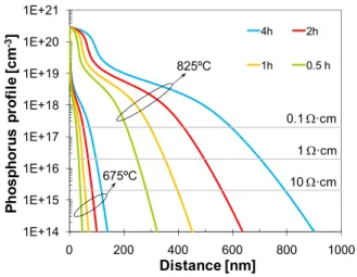
Figure 2. Phosphorus diffusion profiles in silicon for times ranging from 0.5h to 4h and temperatures of 675ºC and 825ºC. Horizontal lines represent the background doping of wafers with different resistivity.
PHOSPHORUS DIFFUSION AND SILICON SUBCELL EMITTER DESIGN
When manufacturing a multi-junction solar cell on silicon, one of the first processes to be addressed is the formation of the emitter of the silicon subcell. Essentially, two alternatives exist for this process: 1) the emitter can be grown epitaxially, which implies that the III-V on Si cell will start with the homoepitaxial growth of n-type silicon on the p-type wafer; 2) mimicking what is done on III-V on Ge multijunction solar cell technology, the emitter of the silicon subcell can be formed by diffusion of a group-V element at the initial stages of the heteroepitaxial process.
The use of homoepitaxial growth has demonstrated to be a beneficial factor in the production of high quality GaP layers [2,3], though introduces an additional degree of complexity in the epitaxial process. However, several groups have also reported high quality GaP layers without homoepitaxial silicon buffers [1, 4]. Accordingly, we will focus on this strategy and consider the formation of the emitter from diffusion (as indicated in figure 1) as is the case in conventional triple-junction solar cells based on germanium.
Phosphorus diffusion in crystalline silicon is a well known phenomenon which has been thoroughly studied in the past 40 years [9]. However, the formation of the n++ emitter in the silicon subcell in a MOVPE environment is a complex process somewhat dissimilar to the traditional diffusion step in conventional PV technology. In a MOVPE reactor, at the initial stage (pre-nucleation) several phosphorus compounds may coexist depending on the process followed and the temperature used: atomic P desorbed from the reactor walls and susceptor; PH3 intentionally injected and the byproducts of its pyrolysis (PH2). All these compounds interact with the wafer surface to provide a final coverage of P dimmers. As a result of a given phosphorus surface coverage at the elevated temperatures characteristic of the MOVPE process,
diffusion of P into the wafer takes place. In a second stage (in a process without a silicon homoepitaxial buffer), GaP nucleation starts while still an important phosphorus supply remains as a result of interdiffusion between the epilayer and the silicon substrate. Finally, in a third stage, during the growth of the graded buffer and the top subcell (figure 1), the diffused phosphorus further penetrates into the substrate. In summary, the final junction depth will be combined result of these processes.
In order to have a first estimate of the emitter P profile and thickness, diffusion models for phosphorus in silicon have been implemented considering the various mechanisms (vacancy-mediated diffusion at high P concentrations and an interstitially driven diffusion at lower P concentrations) that give rise to the typical kink-and-tail profiles [9]. The simulations only consider three independent parameters: diffusion temperature, time and phosphorus concentration at the surface; and have been calculated considering an unlimited phosphorus supply during the whole process (which might not be the case for all situations in a MOVPE reactor) due to the balance between P and H in the surface coverage [10]. Figure 2 shows an example of the diffusion profiles simulated for two different temperatures (675ºC and 825ºC) and times ranging from 0.5h to 4h. These temperatures define two characteristics cases for the temperatures involved in the growth of the III-V silicon. Typically, an initial short time (0.5-1 hour) anneal at high temperatures (820-1050ºC) takes place to desorb the oxide and to create the double step configuration that avoids the formation of antiphase domains. In some recipes, a GaP nucleation layer is also grown at this high temperature range [1]. A temperature of 825ºC can be seen as lower limit for this high temperature regime, though higher temperatures seem to be needed for a complete removal of the oxide layer in a MOVPE environment [11]. In a subsequent stage, the growth of the III-V layers takes place for some hours (1-4) at significantly lower temperatures (500-675ºC). A temperature of 675ºC could represent a typical maximum temperate for this step. As shown by figure 2, which aims to provide a visual appraisal of the impact of diffusions taking place at these two limiting cases, the penetration of phosphorus at temperatures of 675º (or lower) will be very shallow even for long times, whilst yet short anneals at 825ºC will cause P diffusions with much deeper penetration both for the saturation and tail regions. The actual junction depth will depend on the original wafer doping (resistivity) as indicated by horizontal lines in figure 2. In summary, figure 2 indicates that phosphorus exposure during the high temperate pre-nucleation phase, either intentional (PH3 flush) or unintentional (P background pressure in the reactor), may be the determinant step in terms of emitter formation in the silicon sub-cell.
the experimental free electron concentration as measured by ECV. For conventional silicon technology, the chemical and the electrical concentration overlap for concentrations below 1020 cm-3, so electrical activation of P cannot account for this huge difference. It seems that the origin of this difference is fundamentally linked to the phosphorus surface concentration used in the calculations (2·1020 cm -3), which is roughly an order of magnitude higher than the
values measured (3·1019 cm-3). These values are in agreement with other studies using PH3 as the dopant source [12] and maybe the result out-diffusion, impact of atomic hydrogen in the diffusion, or of the self-limiting nature of the adsorption process of phosphorus on the silicon surface. This self-limitation causes that the saturation of the surface coverage with phosphorus can be attained with rather low PH3 flows. Higher PH3 flows do not increase the surface coverage (i.e. the P surface concentration) as shown by figure 3, in which the profiles obtained with 100 sccm and 450 sccm are virtually identical for the initial part of the profile (x<80nm) where lower error is to be expected.
1,E+15 1,E+16 1,E+17 1,E+18 1,E+19 1,E+20 1,E+21
0,000 0,025 0,050 0,075 0,100 0,125 0,150 0,175 0,200 Theory [1h @825ºC] 450 sccm [1h @825ºC] 100 sccm [1h @825ºC]
F
ree
el
e
ct
ron
c
o
nc
e
nt
rat
ion
[c
m
-3]
Depth [µm]
Figure 3. ECV Profiles measured on silicon wafers annealed at 825ºC under different flows of PH3. The expected theoretical profile is included as a solid line. White symbols represent experiments conducted at 100 mbar with a total reactor flow of 14 slpm
Figure 4 shows some simulations made using PC1D for the internal quantum efficiency (IQE) of silicon solar cells with the emitter profiles shown in figure 2 for diffusions at 825ºC on a substrate with a resistivity of 1 Ω·cm. The absorption edges for three different GaAsP compositions for the top cells –namely, GaAs0.6P0.4, GaAs0.7P0.3 and GaAs0.8P0.2− are also indicated in the figure. This figure shows that the region (shadowed in gray) where the differences in IQE are apparent due to the different emitter designs lies above the absorption edge of any of the GaAsP compositions considered. Thereby, as in a tandem configuration only the high-wavelength part of the spectrum reaches the bottom subcell, its effective IQE will be basically independent of the P diffusion depth. In other words, the short circuit current attained by the bottom subcell will be basically determined by the cell base (i.e.
the p-type silicon substrate), provided that the MOVPE environment introduces no significant degradation of its SRH lifetime. Therefore, the emitters formed by P diffusion need to be thick enough to minimize the risk of shunts, while still thin for the maximization of open circuit voltage through the minimization of emitter saturation currents.
Figure 4. Simulated internal quantum efficiency of a Si solar cell with the emitter profiles shown in fig. 2 for diffusions at 825ºC on a substrate with resistivity of 1
Ω·cm. Absorption edges for three different GaAsP compositions of the top cells are indicated
SURFACE MORPHOLOGY
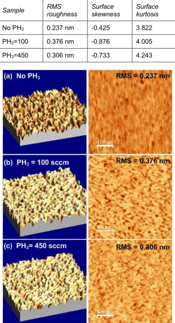
A side effect of the diffusion process can be the degradation of the substrate surface morphology. It has been described that exposure of silicon (100) surfaces to PH3 may result in roughening of the surface due to silicon hydridation and subsequent dimmer displacement [13, 14]. Other authors have also observed the formation of SiP compounds [15]. Roughening and foreign species typically generate antiphase disorder and other crystallographic defects in the GaP nucleation layer, which grows exhibiting poor morphology and thus limiting the quality of the active layers of the device. Consequently, the optimum diffusion conditions for the formation of the bottom subcell emitter have to be attained without degrading the morphology of the substrate.
which should be zero for a morphology consisting of evenly distributed peaks and valleys of homogeneous heights– is negative in the three cases, indicating that the samples present larger valleys (holes) than peaks. Surface kurtosis also increases with PH3 anneal suggesting a transition to a spikier surface.
Table I: Roughness parameters of the AFM scans included in Fig 5.
Sample RMS roughness Surface skewness Surface kurtosis
No PH3 0.237 nm -0.425 3.822
PH3=100 0.376 nm -0.876 4.005
PH3=450 0.306 nm -0.733 4.243
Figure 5. AFM topography scans of silicon wafers annealed at 825ºC for 60 min. under different PH3 flows. The images in the right column are plain views and the images on the left are 3D representations of the same image. (a) No PH3; (b) 100 sccm of PH3; (c) 450 sccm of PH3. RMS roughness for each case is indicated on the top-right corner of each scan.
Figure 6. (a)STEM image of a GaP layer grown on silicon; (b) HRSTEM detail of the GaP/Si interface ; and (c) TEM detail of the GaP/Si interface
GaP PASSIVATION OF THE SILICON EMITTER
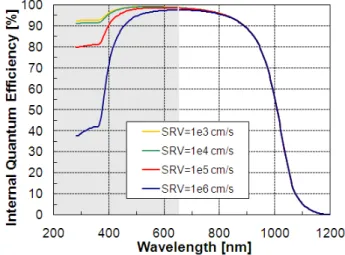
A final aspect being evaluated is the quality of the passivation provided by the GaP nucleation layer to the emitter of the silicon subcell. Emitter passivation is an important issue in conventional crystalline silicon solar cell technology though it might not be so critical for the III-V-on-silicon dual-junction solar cell due to the limited amount or high energy photons reaching the bottom subcell after the absorption in the upper layers. Figure 7 shows the internal quantum efficiency –simulated with PC1D– as a function of emitter surface recombination velocity (SRV) of a silicon solar cell with the emitter profiles shown in figure 2 for a diffusion of 60 min at 825ºC on a substrate with resistivity of 1 Ω·cm. The wavelengths shadowed in gray in the figure would be filtered by a GaAs0.8P0.2 top cell. Accordingly, from 650 nm onwards the IQE seems unaffected by changes in three orders of magnitude in the emitter surface recombination velocity (all curves virtually overlap in this range). Thereby, emitter SRV is a parameter with little impact in the short circuit current of the bottom subcell, though it may impact the open circuit voltage through the emitter dark saturation current. The experimental characterization of the SRV at the GaP/Si interface is ongoing using Photoconductive Decay (PCD) and will be presented in future works.
Figure 7. Simulated internal quantum efficiency as a function of emitter surface recombination velocity of a silicon solar cell with the emitter profiles in figure 2 for a diffusion of 60 min at 825ºC on a substrate with resistivity of 1 Ω·cm. Wavelengths shadowed in gray would be filtered by a GaAs0.8P0.2 top cell.
SUMMARY AND CONCLUSIONS
The integration of III-V materials on silicon may provide a cost breakthrough for photovoltaic technology, unifying the low cost of silicon and the efficiency potential of III-V multijunction solar cells. Dual-junction solar cells formed by a GaAsP or GaInP top cell and a silicon bottom cell
seem to be excellent candidates for this integration and thereby have been intensely investigated in recent years. In this study, we analyze several factors influencing the performance of the bottom subcell of this dual-junction. To study the formation of the silicon subcell emitter we have implemented phosphorus diffusion models that consider vacancy-mediated diffusion at high P concentrations and an interstitially driven diffusion at lower P concentrations and thus are able to reproduce typical kink-and-tail profiles observed for P in Si. This model is being applied to the analysis of different diffusion experiments during the growth of GaP nucleation layers on silicon in a MOVPE reactor. Preliminary experiments reveal that the P diffusion actually taking place is less intense than predicted presumably as a result of a lower phosphorus surface concentration achievable when doping from a gas phase. AFM measurement indicate that some degradation of the morphology occurs when exposing the wafers to PH3 for diffusion , though the RMS roughness values measured seem tolerable for the growth of high quality nucleation layers. Finally, some simulations have been made to assess the impact of different surface recombination velocities for the GaP/Si interface on the internal quantum efficiency of the silicon bottom subcell. These simulations show that the influence of such interface is negligible for practical dual-junction designs since the top cell absorbs the wavelength range affected.
ACKNOWLEDGEMENTS
The authors are deeply indebted to Dr. Jasmin Hofstetter for her assistance with the simulation of the phosphorus profiles. AFM images included in this work were taken at the Centre for Electronic Microscopy “Luis Bru” (Universidad Complutense de Madrid) with the kind assistance of Mrs. Ana Soubrie. TEM analysis was conducted at the Instituto de Nanociencia de Aragón (Universidad de Zaragoza) under the guidance of Dr. Rodrigo Fernández-Pacheco y Dr. Alfonso Ibarra. This work is supported by the Spanish Ministerio de Ciencia e Innovación under the CONSOLIDER-INGENIO 2010 program by means of the GENESIS FV project (CSD2006-004) and research projects with references TEC2009-11143, TEC2008-01226 and PSS-440000-2009-30. The Comunidad de Madrid has also contributed under the NUMANCIA II program (S2009/ ENE1477) and with project CCG10-UPM/ENE-566.
REFERENCES
[1] Y. Takano, T. Takagi, Y. Matsuo, and S. Fuke, "Surface Evolution of GaP Grown on Si Substrates Using Metalorganic Vapor Phase Epitaxy", Japanese Journal of Applied Physics 49 (2010) 035502
[3] T.J. Grassman, M. R. Brenner, S. Rajagopalan, R. Unocic, R. Dehoff, M. Mills, H. Fraser, and S. A. Ringel, “Control and Elimination of Nucleation-Related Defects in GaP/Si(001) Heteroepitaxy” Applied Physics Letters, 94, 232106, (2009).
[4] J. F. Geisz, J.M. Olson, M.J. Romero, C.S. Jiang, A.G. Norman, "Lattice-mismatched GaAsP Solar Cells Grown on Silicon by OMVPE", 4th World Conference on Photovoltaic Energy Conversion (2006), pp.772-775
[5] T J. Grassman, M. R. Brenner, M. Gonzalez, A. M. Carlin, R. R. Unocic, R. R. Dehoff, M. J. Mills, and S. A. Ringel, "Characterization of Metamorphic GaAsP/Si Materials and Devices for Photovoltaic Applications", IEEE Transactions on Electron Devices, 57 (10) pp. 3361-3369
[6] T. Roesener, H. Döscher, A. Beyer, S. Brückner, V. Klinger, A. Wekkeli, P. Kleinschmidt, C. Jurecka, J. Ohlmann, K. Volz, W. Stolz, T. Hannappel, A.W. Bett, F. Dimroth, "MOVPE Growth of III-V Solar Cells on Silicon in 300 mm Closed Coupled Showerhead Reactor", 25th European Photovoltaic Solar Energy Conference and Exhibition, Sept. 2010, (Valencia, Spain) pp. 964 - 968
[7] A. Ishizaka and Y. Shiraki, “Low temperature cleaning of Silicon and its application to Silicon MBE”, J. Electrochem. Soc.: Electrochemical Science and Technology, 133, n 4, pp. 666-671, 1986
[8] I. Horcas, R. Fernández, J.M. Gómez-Rodríguez, J. Colchero, J. Gómez-Herrero, A.M. Baro, “WSXM: A software for scanning probe microscopy and a tool for nanotechnology”, Rev. Sci. Instrum. 78 (2007) 013705.
[9] A. Bentzen, A. Holt, J.S. Christensen y B.G. Svensson, “High concentration in-diffusion of phosphorus in Si from a spray-on source”, J. Appl. Phys., 99, 2006, 064502
[10] Y. Tsukidate, M. Suemitsu, “Saturated adsorption of PH3 on Si(100):P and its application to digital control of phosphorus coverage on Si(100) surface”, Applied Surface Science 151 (1999) pp.148–152
[11] H. Döscher, S. Brückner, T. Hannappel, “Investigation of oxide removal from Si(100) substrates in dependence of the MOVPE process gas ambient”, Journal of Crystal Growth 318 (2011) 563–569
[12] B. Kalkofen, M. Lisker, E. P. Burte, “Phosphorus diffusion into silicon after vapor phase surface adsorption of phosphine”, Materials Science and Engineering B 124– 125 (2005) 288–292
[13] D.-S. Lin, T.-S. Ku, T.-J. Sheu, "Thermal reactions of phosphine with Si(100): a combined photoemission and scanning-tunneling-microscopy study", Surface Science 424 (1999) pp. 7–18
[14] Y. Takano, T. Okamoto, T. Takagi, S. Fuke, “Influence of PH3 Preflow Time on Initial Growth of GaP on Si Substrates by Metalorganic Vapor Phase Epitaxy”, IEICE Transactions on Electronics, Volume E92.C, Issue 12, pp. 1443-1448 (2009)