Abstract—A methodology for the analysis and synthesis of multiple hysteresis loops in the frequency characteristic of a voltage-controlled oscillator (VCO) is presented. This is achieved through the coupling of an oscillator inductance to multiple external (passive) resonators, with resonant frequencies in the tuning range of the VCO. A possible application to the implementation of a compact chipless Radio Frequency Identification (RFID) system is explored, using the oscillator as a reader and placing the external resonators in the tag. The system takes advantage of the high sensitivity to the tag resonances in the presence of hysteresis, which leads to vertical jumps in frequency versus the tuning voltage. A desired bit pattern would be encoded in the tag by enabling or disabling passive resonances at a sequence of frequencies. In the practical realization, the inductors in the oscillator and the external board are implemented through spiral inductors so that the resonators in the VCO and the tag have strong broadside coupling. The coupling effect is modeled through electromagnetic simulations, from which a linear admittance, representing the coupled subnetwork, is extracted. The multi-hysteresis oscillator characteristic can also be obtained experimentally through a new methodology able to stabilize the physically unstable sections without altering their steady-state values. Different demodulation methods for reading the tag are discussed.
Index Terms— Arc-length continuation, hysteresis, oscillator, measurement techniques, simplicial decomposition.
I. INTRODUCTION
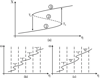
Hysteresis [1]-[4] is often observed in nonlinear circuits (both autonomous and driven) such as voltage-controlled oscillators, injection-locked oscillators and power amplifiers. It is due to the coexistence of stable solutions in a certain parameter interval. In a typical hysteresis (between two stable solutions of the same kind), the solution curve exhibits three coexisting sections and two turning points [1]-[4], as shown in the sketch of Fig. 1(a), where a representative variable X (e.g. a voltage amplitude or the oscillation frequency, in an autonomous circuit) is represented versus the parameter . Sections 1 and 3 are stable, whereas section 2 (in a dashed
This work was supported in part by the Spanish Ministry of Economy and Competitiveness and the European Regional Development Fund (ERDF/FEDER) under research project TEC2017-88242-C3-1-R.
This paper is an expanded version from the IEEE MTT-S International Microwave Symposium (IMS 2019), Boston, MA, USA, June 2-7, 2019.
A. Suárez and F. Ramírez are with the Communications Engineering Department, University of Cantabria, 39005, Santander, Spain (e-mail: [email protected]; [email protected]).
R. Melville is with is with EMECON, LLC, Berkeley Heights, NJ, USA, (e-mail: [email protected]).
line) is unstable and, thus, cannot be physically observed. When increasing (decreasing) the parameter from a low (high) value the circuit initially operates in section 1 (section 3) and jumps to section 3 (section 1) at the turning point T1 (T2). In most cases, the hysteresis is due to an expansion of the circuit negative resistance in a certain interval of the excitation amplitude [5], which enables the fulfilment of the steady-state conditions for three distinct amplitude values. In most previous works, hysteresis was undesired, so several simulation tools [1]-[3] were proposed for its accurate prediction at the design stage.
In harmonic balance (HB) [1]-[3],[6],[7] the circuit variables are represented as a Fourier series, whose coefficients constitute the unknowns of a nonlinear algebraic system, solved numerically. Unlike standard time-domain integration [8], the HB method is insensitive to the physical stability properties of the solution, so with the aid of complementary techniques [1]-[3], it is able to provide the complete solution curve in Fig. 1(a), including the unstable section 2. In the absence of these techniques, when just sweeping the parameter, one obtains either discontinuous jumps or a loss of convergence in the neighborhood of the turning points, where the Jacobian matrix of the HB system becomes singular [1]-[3]. To circumvent this problem, the works [3], [9]-[11] make use of a continuation method, based on the introduction of an auxiliary generator (AG) into the circuit, which enables a simple implementation of a parameter-switching continuation technique [2]. In [12] a mathematical condition, fulfilled at the turning points, is derived, which enables a direct calculation of these points. The works [13]-[14] take a different approach using a contour-intersection method, applied to an outer-tier admittance function extracted from HB. On the other hand, the work [15] addresses the experimental characterization of the full hysteresis loop in driven circuits. This requires the stabilization of section 2 [in the sketch of Fig. 1(a)] without altering its steady-state values.
The recent work [16] describes a hysteresis phenomenon obtained through the coupling of a free-running oscillator to an external resonator. This behavior had been observed in the so called “dip oscillator” [17]-[18], which exhibits an amplitude change when weakly coupled to a passive resonant circuit, tuned to its free-running frequency. When increasing the coupling, hysteresis is obtained versus the tuning parameter, which, as shown in this work, is due to a multi-resonance behavior about the original free-running frequency. As also shown here, this kind of hysteresis is easy to control and several distinct hysteresis loops can be synthesized in the
Analysis and Synthesis of Hysteresis Loops in
an Oscillator Frequency Characteristic
Almudena Suárez, Fellow, IEEE, Robert Melville, Senior Member, IEEE, and Franco Ramírez, Senior
oscillator frequency characteristic. This can be relevant to chipless radiofrequency identification (RFID) [19]-[23] because the vertical jumps [Fig. 1(a)] give rise to a distinct oscillator response to the external resonators. As another example, in a sensor/actuator, the core oscillator would contain the sensing capacitance and the hysteresis cycles, induced by the coupling to the external resonators, would give rise to an upward or downward frequency jump when this capacitance exceeds or goes below certain levels. The upward/downward jump in a given cycle would provide a control signal to turn on or off a particular switch.
This work extends [16] with an in-depth analysis of the oscillator behavior under the effect of several coupled resonators. Multiple hysteresis loops are synthesized in a controlled fashion, for the first time to our knowledge, and the possible application to chipless RFID systems is studied. This implementation will be based on the principle described in [22], where the impedance of the tag influences the frequency of a sweep-tuned oscillator, acting as a reader. Then, the tag bit pattern is detected from the subsequent change to the DC bias current. Unlike the present approach, no hysteresis is involved. In [23] a detailed analysis and simulation of the system in [22] is presented, considering chipless tags with orthogonally-polarized antennas [21]. A practical limitation may be the small impact of the tag resonances on the oscillator frequency. Here the possibility to increase the reading sensitivity by inducing hysteresis, and hence physical jumps, in the oscillator characteristic is explored. The aim will be to use hysteresis loops to encode the bit pattern of the tag. As will be shown, this procedure enables a much more distinct signal for the individual bits encoded by the passive tag than the one resulting from ordinary resonances.
“1” “0” “1” “0” “1” “1” “1” “1” 1 T1 T2 X (b) (c) (a) 2 3
Fig. 1. Sketch of the hysteresis phenomenon. (a) Typical hysteresis loop between two solutions of the same kind. (b) Bit pattern “1111” implemented through hysteresis loops. (c) Bit pattern “1010”.
The hysteresis loops are synthesized according to the desired bit pattern of the tag, which is encoded by enabling or disabling the resonators that give rise to the distinct hysteresis loops. For instance, Fig. 1(b) and Fig. 1(c) shows the expected responses for “1111” and “1010”, where is the oscillation frequency. Each hysteresis loop occurs in a distinct parameter
interval, as shown in the sketch of Fig. 1. Otherwise, in the same parameter interval there could be more than two stable solutions. In the RFID application considered in the paper, this would give rise to uncertainty in the tag reading. Different methods of detecting the encoded bit pattern ("reading" the tag) with different sensitivities and circuit complexities are discussed.
The paper is organized as follows. Section II presents an analytical investigation of the multi-hysteresis mechanism. Section III describes the analysis of the oscillator coupled to the resonators in the external board. Section IV presents the experimental characterization of the hysteresis cycles. Section V discusses the implementation of the tag reader.
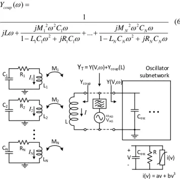
II. MULTI-HYSTERESIS MECHANISM A. Oscillator Equation
Let us consider an oscillator loaded with a resonant circuit composed by of an inductor L and a capacitor Cosc, as shown in Fig. 2. Now, the oscillator will be placed near a number N of external resonators, each one composed of an inductor, capacitor and resistance Ln, Cn and Rn, where n = 1 to N. It is assumed that the inductors Ln can be coupled to the oscillator inductor L. A periodic solution is assumed and the system will be analyzed at the fundamental frequency. The oscillator circuit, excluding the coupled inductor L, will be described in terms of the admittance function Y(V,), as shown in Fig. 2, where V and are, respectively, the excitation amplitude and frequency. Then, the oscillator is governed by the following equations: ( , ) ( , ) 0 T Y V V Y V V I (1) 1 1+ + 2 2 N N V jL I jMI jM I jM I (2) where YT is the total admittance, calculated between the terminals of the inductor (L) in the oscillator circuit, as indicted in Fig. 2, I is the current circulating through L, In is the current through the inductor (Ln) of each of the external resonators and Mn (n = 1 to N) are the coupled inductances, related with the coupling factors kn as Mn kn L Ln . The currents In through the external resonators are calculated from:
1 1 1 1 1 2 2 2 2 2 1 0 1 0 1 0 N N N N N jM I R jL I jC jM I R jL I jC jM I R jL I jC (3)
Note that the coupling among the external resonators themselves has been neglected, which, as demonstrated in Section III, constitutes a reasonable approximation. Each of the equations in (3) can be solved for the particular current, I1 to IN, in terms of I. This provides:
1 n n n n n M I j I R jL jC (4)
The above expression relates the current through each resonator (Ln, Cn and Rn) to the induced voltage jMnI. Replacing (4) for I1 to IN in the expression for V in (2) and this, in turn, in the main oscillator equation (1), one obtains:
( , ) ( , ) ( ) 0
T coup
Y V Y V Y (5)
where Ycoup( ) is the input admittance seen from the terminals of the oscillator inductor L (Fig. 2), in the presence of the whole set of coupled resonators:
2 2 2 2 1 1 2 2 1 1 1 1 ( ) 1 ... 1 1 coup N N N N N N Y jM C jM C jL L C jR C L C jR C (6) L1 L2 LN C1 C2 CN R1 R2 RN M1 M2 MN L Ycoup Y(V,) Cosc Oscillator subnetwork i(v) = av + bv3 i(v) + V ‐ Cosc R YT = Y(V,)+Ycoup(L) I I1 I2 IN AG VAG
Fig. 2. Sketch of the generic oscillator with an inductance L coupled to multiple external resonators. The exemplary case of a Van der Pol oscillator is considered, with the parameters a = -0.03 A/V, b = 0.01 A/V2, R = 200 ,
Cosc = 86 pF. The auxiliary generator used for simulation purposes is also represented.
For a compact expression of Ycoup it is possible to define the following impedance terms Zn( ) , where n = 1 to N:
2 2 2 ( ) 1 n n n n n n n jM C Z L C jR C (7)
Then, (5) can be rewritten as:
1 ( , ) ( , ) ( ) 1 ( , ) 0 ( ) ... ( ) ... ( ) T coup n N Y V Y V Y Y V jL Z Z Z (8)
Assuming small values of the coupled inductances M1 to Mn, one can perform a Taylor-series expansion of the second term in (8) about 1/(jL). This provides the following approximate expressions:
1
2 1 1 ( ) ( ) ... ( ) ... ( ) ( ) coup n N Y Z Z Z jL L (9)which can be used to obtain an approximate version of equation (8):
1
2 1 ( , ) ( , ) 1 ( ) ... ( ) ... ( ) 0 ( ) T n N Y V Y V jL Z Z Z L (10)At this point, it is interesting to note that ( ) / ( )2
n Z L can be expressed as: 2 2 2 2 ( ) ( ) 1 n n n n n n n Z M jC L L L C jR C (11)
Then, (10) can be rewritten as:
2 1 2 1 1 1 2 2 1 1 ( , ) ( , ) 1 1 ... 0 1 T N N N N M Y V Y V jL L R jL jC M L R jL jC (12)
Thus, under weak coupling, the oscillator behaves as if it were loaded with N series subnetworks, connected in parallel between the coupling node and ground. As also gathered from (11), there is a scaling effect, due to the constant coefficients
2/ 2
n
M L .
If the resonance frequencies n are too closely spaced, neighboring resonators may significantly affect one another. In this situation, the Taylor series expansion in (9) may not be accurate enough, due to the large magnitude excursions of the total coupled impedance Z1( ) ... ZN( ) . In order to avoid this problem, the frequency spacing must be larger than the bandwidth of the resonators in (12), depending on their individual Q factors Lnn/Rn. In these conditions, the coupled oscillator can be analyzed by splitting (12) into real and imaginary parts:
2 2 2 2 2 2 1 2 2 2 2 2 2 1 ( , ) ( , ) ( ) ( , ) (a) 0 1 ( , ) ( , ) ( ) 1 ( , ) (b) 1 0 1 r r r T coup r N n n n n n n n n i i i T coup i N n n n n n n n n n Y V Y V Y Y V R C M L L C R C Y V Y V Y Y V L C L C M L L C R C
(13)where the superscripts “r” and “i” respectively indicate real and imaginary part. As gathered from (13) the coupling to the external resonators affects both the real and imaginary parts of the total admittance function YT.
B. Multi-Resonance Effects
To illustrate the multi-resonance effects, a computational test has been performed, considering the coupling of an inductor L to six external resonators. The inductance values are L = Ln = 450 nH. The capacitors C1 to CN are calculated to obtain equally spaced resonances going from 30 MHz to 40 MHz. The coupling factor is the same for all the resonators,
k = kn n, and given by: k = 0.025. Initially, the resonator resistance is R = Rn = 1 . In Fig. 3(a), the red solid curve corresponds to i ( )
coup
Y and the blue dashed curve corresponds to 1/ L . As gathered from the inspection of (13b), for < 1, the first resonance at 1 tends to shift the curve i ( )
coup
Y upwards (with respect to 1/ L ), due to the positive value of 2
1 1
1 L C . On the other hand, for > N, the last resonance at N pushes the curve downwards, due to the negative value of 1 2
N N
L C
. For the middle resonances, 2 to N , the two effects are approximately balanced. 1
28 30 32 34 36 38 40 42 Frequency (MHz) -0.012 -0.01 -0.008 28 30 32 34 36 38 40 42 Frequency (MHz) -0.012 -0.01 -0.008 im ag (Yac o p ) ( -1 )i m ag (Yac o p ) ( -1 ) (a) (b) Free-running Free-running R = 1 R = 2 Resonances overlap Fig. 3. Variation of i ( ) acop
Y in (13b) for L = Ln = 450 nH under two different
quality factors. (a) Parasitic resistance R = 1 . The minima and maxima of the higher-frequency resonances are overlapped. (b) Parasitic resistance R = 2 . Distinct resonances and no overlapping of maxima and minima.
As shown in the next subsection, to avoid the overlapping of the hysteresis cycles, the maximum of i ( )
coup
Y about each resonance n must be smaller than the minimum of i ( )
coup
Y about the next resonance n+1. This non-overlap condition is violated in Fig. 3(a), since the maximum of the fifth resonance is higher than the minimum of the sixth one. When
considering the full oscillator circuit [instead of i ( ) coup
Y only] this will give rise to more than three steady-state solutions coexisting for the same parameter values (overlapping of the hysteresis cycles). The overlapping in Fig. 3(a) is due to the high Q resulting under R = Rn = 1 . On the other hand, for excessively low Q, each resonator Ln, Cn and Rn will not give rise to a sufficient difference between the maximum and minimum induced by this resonator on the susceptance
( ) i coup
Y . As a compromise, Fig. 3(b) presents the results obtained for R = 2 (hence lower Q), with clearly distinguished extremes (maximum and minimum) about each resonance frequency of the external resonators. Note that n there is no overlapping of the full set of maxima and minima.
C. Multiple Hysteresis Cycles
To get insight into the impact of the coupling effects on the oscillator characteristic, only one resonator will be initially considered in (13), with the associated impedance term
( ) n
Z . The real and imaginary parts of the total oscillator admittance (YT) are given by:
2 2 2 2 2 2 2 2 2 2 2 2 ( , ) ( , ) 1 1 ( , ) ( , ) 1 0 1 n n r r n T n n n n i i T n n n n n n n n R C M Y V Y V L L C R C Y V Y V L C L C M L L C R C (14)As stated, the coupling effects introduce a scaled version of the admittance of the series network Rn, Ln, Cn (in parallel between the analysis node and ground). For better clarity, the simple Van der Pol oscillator in Fig. 2 will be initially considered. The oscillator admittance Y V( , ) (excluding L)
is ( , ) 3 / 4 2
osc
Y V a bV jC . Suitable values for the
parameters a and b are given in the caption of Fig. 2. In these conditions, system (14) simplifies to:
2 2 2 2 2 2 2 2 2 2 2 2 2 3 ( , ) 0 4 1 1 ( ) 1 0 1 n n r n T n n n n i T osc n n n n n n n n R C M Y V a bV L L C R C Y C L C L C M L L C R C (15)Now, the oscillator will be tuned by varying Cosc. It is assumed that for the particular capacitor value Cosc,n, and in the absence of coupling effects (Mn = 0), the oscillation frequency is n 1/ L Cn n . In the presence of coupling effects (Mn ≠ 0), the imaginary part YTi( ) will be zero at
1/ n L Cn n
. Hoverer, i( ) T
additional frequencies, below and above , as easily n gathered from (15). Replacing the three frequencies in
( , ) r T
Y V one obtains three different amplitude values, one for each frequency, which explains the hysteresis induced by linear coupling effects. Note that, in the general case (14), the amplitude dependence of the imaginary part i( , )
T
Y V , will give rise to a small deviation from the original free running frequency n.
Now, the Van der Pol oscillator will be analyzed in the presence of N coupled resonators. This is done by replacing
2
( , ) 3 / 4 osc
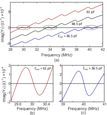
Y V a bV jC into (13). Evaluating YTi( ) for distinct values of Cosc (acting as the tuning parameter) one obtains the curves in Fig. 4(a). The Cosc values considered are 36.5 pF, 48.5 pF and 61 pF. Increasing Cosc one basically shifts upwards the imaginary part i( )
T
Y . For some intervals of Cosc, there will be three crossings through zero of YTi( ) , as a result of the particular shape of i ( )
coup
Y . In Fig. 4(b) an expanded view of the curve corresponding to Cosc = 61 pF about f1 = 30 MHz is presented. This demonstrates three roots of i
T
Y about this frequency. Fig. 4(c) presents an expanded
view of the curve corresponding to Cosc = 36.5 pF about f6 = 40 MHz. 28 30 32 34 36 38 40 42 Frequency (MHz) -5 0 5 im ag (YT ) ( -1 ) ×1 0 -3 (a) 48.5 pF Cosc = 36.5 pF 61 pF 29.6 30 30.4 Frequency (MHz) -2 -1 0 1 2 im ag (YT ) ( -1 ) ×1 0 -4 (b) Cosc = 61 pF (c) 40 41 Frequency (MHz) -4 -2 0 2 4 Cosc = 36.5 pF 39
Fig. 4. Imaginary part of the total oscillator admittance in the presence of six external resonators for k = 0.04. (a) Variation of i
T
Y for three distinct values
of Cosc, given by 36.5 pF, 48.5 pF and 61 pF. (a) Cosc = 61 pF. Expanded view. There are three solutions of i 0
T
Y about 30 MHz. (b) Cosc = 59 pF. Expanded
view. There are three solutions of i 0
T
Y about 40 MHz.
In the presence of the six external resonators, and under variations of Cosc, one obtains six hysteresis cycles. This can
be seen in Fig. 5. For good accuracy the curve has been obtained in commercial harmonic balance (Keysight Advanced
Design System) [1]-[3],[6],[7] with a number (NH) of
harmonic terms NH = 7, introducing an auxiliary generator (AG) into the circuit [3], [9]-[11], as shown in Fig. 2. The AG is an independent voltage source in series with an ideal bandpass filter, operating at the oscillation frequency AG = and amplitude VAG (both must be determined in the analysis procedure). The AG is connected in parallel at a sensitive circuit node (Fig. 2), such as a device terminal, and must fulfill a non-perturbation condition [2]-[3], given by the zero value of the ratio between the AG current and voltage
YAG = IAG/VAG = 0. In commercial harmonic balance [3], [9], the condition YAG = 0 is achieved through optimization of the AG frequency and amplitude, through it is also possible to optimize other quantities.
The AG allows passing through turning points, which cannot be done through a simple parameter sweep, as indicated in the introduction. This is achieved by switching the analysis parameter to an AG variable (either frequency or amplitude) in the multivalued interval. In the case of Fig. 5, the AG frequency has been swept (which agrees with the oscillation frequency), solving YAG = 0 in terms of the oscillation amplitude, VAG, and the physical parameter Cosc. With this parameter switch, the infinite-slope points become zero-slope points, without any simulation difficulty.
To emphasize the dependence of the hysteresis cycles on the resonance effects induced by the coupling, the value of the capacitor Cosc has been represented versus the AG frequency. This can be compared with the imaginary part of the total admittance, i( )
T
Y , represented on the right axis. In the calculation of the oscillator curve, three different values of the coupling factor have been considered: k = 0.02, 0.04, 0.06. As gathered from the figure, the six multi-valued regions are located about the resonance frequencies of the six external resonators. The excursions due to the resonance minima and maxima increase with the coupling factor and will give rise to overlapping for too high k. Fig. 5(b) shows the oscillation amplitude versus the tuning capacitor Cosc for the same three k values.
To summarize, hysteresis arises because of the particular form of variation of the susceptance about the original oscillation frequency n under weak coupling conditions (see Fig. 4). If the active device can supply negative conductance at the three resonance frequencies, the steady-state oscillation conditions, Re(YT) = 0 and Im(YT) = 0, will be fulfilled at three distinct solution points. This will generally be the case, since the device will exhibit negative conductance in a certain frequency band and the two additional resonant frequencies [at which Im(YT) = 0] are close to the original one. The condition Re(YT) = 0 will be fulfilled for a different amplitude in each case, since, due to the coupling, Re(YT) exhibits a frequency dependence.
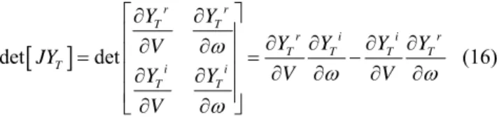
Regarding the stability properties, as shown in [3], the oscillator exhibits a dominant real pole proportional to
det[JYT]
det det r r T T r i i r T T T T T i i T T Y Y Y Y Y Y V JY V V Y Y V (16)and [JYT] is the Jacobian matrix of the admittance function YT with respect to the two state variables V and . Expression (16) formally agrees with the one derived in [24] under a fundamental-frequency analysis. Thus, the solution will exhibit a negative dominant real pole for det[JYT] 0 ,
corresponding to the stability condition derived in [24]. In general, the second term of det[JYT] in (16) is much lower
than the first term. In most cases, the standalone oscillator will fulfill: r / 0, i / 0
T T
Y V Y
. First condition implies a reduction of negative conductance with the excitation amplitude, as occurs in all physical devices from a certain amplitude value, and second condition implies an increase of the susceptance with frequency as in a Foster network. Under weak coupling to an external resonator, one will have three steady-state solutions, as explained above. Due to the form of variation of the susceptance (Fig. 4), one will have
/ 0
i T
Y
at the original oscillation. Because the coupled resonator is linear and the coupling is weak, this coupling will have only a small effect on the total conductance. Thus, the coupling will destabilize the original oscillation and will give rise to two stable oscillations at a higher and lower frequency, having /i 0 T Y . 28 30 32 34 36 38 40 42 Frequency (MHz) 60 80 100 120 60 70 80 90 100 110 Capacitance Cosc (pF) 2 2.05 2.1 -0.012 -0.01 -0.008 im ag ( YT ) ( -1 ) Ca pa ci ta nc e C os c (p F ) A m pl itud e ( V ) (a) (b) k = 0.02 0.04 0.06
Fig. 5. Oscillator solution curve. (a) The value of the tuning capacitor Cosc has
been represented versus the AG frequency, agreeing with the oscillation frequency. The imaginary part of the total admittance, i( )
T
Y , has been
represented on the right axis. In the calculation of the oscillator curve, three different values of the coupling factor have been considered: k = 0.02, 0.04, 0.06. (b) Oscillation amplitude versus the tuning capacitor, Cosc, for the three k
values.
The edges of the multi-valued regions of the oscillator solution curve are determined by a turning-point condition [3],
[12] at which the Jacobian matrix of the oscillator equations becomes singular. In terms of the total admittance function, this singularity condition is given by:
( , ) 0 det 0 T r i i r T T T T T Y V Y Y Y Y JY V V (17)As gathered from the previous study, the sign of the derivative
/ i T
Y
will undergo two changes about each resonant frequency n. It will change from positive to negative and then to positive again (Fig. 4). As stated, in ordinary oscillators, the second term in the determinant of (17) is smaller than the first term, so the change of sign of i/
T
Y
will induce determinant zeroes. In the fundamental-frequency analysis of the Van der Pol oscillator, the imaginary part of the oscillator admittance does not depend on the excitation amplitude. Then, condition (17) simplifies to YT 0 and / 0
i T
Y
. Thus, the boundaries of the hysteresis regions are obtained when the minima and maxima of i
T
Y are tangent to the zero axis, in agreement with the inspection of Fig. 4.
III. SYNTHESIS OF THE OSCILLATOR MAGNETICALLY
COUPLED TO THE RESONATORS IN AN EXTERNAL BOARD
In the proof-of-concept implementation, the Colpitts oscillator in Fig. 6, implemented with a bipolar transistor, has been considered. Varactor diodes are used for tuning. The choice of a Colpitts circuit using a bipolar device is convenient for the VHF frequency range (40–50 MHz) of the current experimental setup, but other oscillator topologies could be used as well. The goal will be to obtain four hysteresis cycles in the oscillator tuning range between 40 MHz and 50 MHz. Note, that as reported in [16], the same hysteresis effect has been observed experimentally at a center frequency in excess of 600 MHz. The circuit of Fig. 6 could be extended to sweep over a larger frequency range (e.g., to allow more bits in the tag) with a band-switching arrangement.
As shown in the following, the coupled subnetwork (composed by the oscillator inductor L and the external resonators) can be implemented separately from the oscillator core. This independent design is possible because of the relatively small coupling effects required for a multi-hysteresis curve with no overlapped hysteresis cycles.
A. Implementation of the Resonators
The coupled resonators will be synthesized using planar spiral inductors and lumped capacitors. The planar nature of the inductors is well suited for an RFID tag implementation. Their moderate quality factor will help prevent an undesired overlapping of the maxima and minima of i ( )
coup
Y [as in the case of Fig. 3(a)]. Here it will be assumed that the inductors in all the external resonators are equal, i.e.,
Tag R∞ RN Y(V,,Vtune) Ycoup() (a) (b) C1 18 pF RE 422 C2 18 pF RC 100 RB1 4.7 k Q1 2N3904 D1 MV209 D2 MV209 VCC RB2 10 k LE 820 nH CB 330 pF RD 43 k Vtune L RN L Mn AG
YT = Ycoup() + Y(V,,Vtune)
Fig. 6. Colpitts oscillator with varactor tuning. (a) Schematic. (b) Separation into a coupled network and an oscillator core. The admittance Ycoup( ) is obtained with the electromagnetic simulations of Subsection III.B. The function Y V( , ,Vtune) is calculated with an auxiliary generator.
The spiral geometries required to implement the oscillator inductor L and the inductors Lt in the external board have been initially estimated from the inductance expression based on current sheet approximation [25]-[26]. This depends on the spiral number of turns, average diameter, fill ratio and some constant coefficients, determined by the spiral shape (square, hexagonal, circle…). As stated, four resonances will be synthesized in the range 40 MHz to 50 MHz.
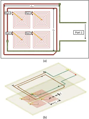
The external inductor value is set to Lt = 474 nH. Fig. 7(a) shows the symmetrical layout of a board with four squared-shaped spiral inductors. These board inductors have nT =7 turns and external and internal diameters dout = 17.5 mm and din = 1 mm, respectively.
The oscillator inductance is L= 469 nH. Although this value is similar to the previous one, it has to be implemented in a different manner to enable near-identical coupling effects in all the inductors of the external board. This is done by reducing the number of turns to nT = 2 and increasing the external and internal diameters to dout = 59.25 mm and din = 52 mm. The whole coupled structure is shown in Fig. 7(b), where the oscillator spiral inductor, with a square shape too, placed over the board inductors, can be noted.
As gathered from the inspection of Fig. 7, the central orthogonal axis of the spirals Lt in the external board exhibits a lateral displacement x = 14.7 mm with respect to that of the spiral L. This will give rise to a reduction in the coupling effects that can be compensated, if needed, by approaching the
inductor L to the external board. The coupling coefficient k of each inductor can be easily estimated following the expressions in [27]. For x =14.7 mm and a vertical distance of 1.5 cm, the estimated coupling coefficient k is 0.02, in the order of those considered in the resonance analysis of Section II.
B. Electromagnetic Simulation of the Coupling Effects
For an accurate calculation of the coupling admittance, an electromagnetic simulation [28] of the coupling of the four spirals in the board and the big-sized spiral is carried out. Initially, a 5×5 scattering matrix describing the whole passive configuration is obtained, defining Port 1 between the terminals of the oscillator spiral and Port 2 to Port 5 at the locations where the capacitors should be connected (at a later stage) to the board spirals. For a distance d = 22.5 mm between the spiral L and the board, the magnitudes of the scattering parameters Sj1, where j = 2 to 5, are shown in Fig. 8, where they have been represented versus frequency. As can be seen, the power transfer is quite similar for all the spirals.
(b) (a) Port 1 Port 2 Port 4 Port 3 Port 5 do ut din din do ut
Fig. 7. Inductors symmetrically arranged in an external board and coupled to the inductor L, corresponding to the oscillator circuit (larger spiral). The board inductors have nT=7 turns and external and internal diameters dout = 17.5 mm and din = 1 mm. The oscillator inductor has nT = 2 turns and
30 35 40 45 50 55 60 Frequency (MHz) -36 -34 -32 -30 -28 |Sj1 | ( d B ) d = 22.5 mm S21 S51 S41 S31
Fig. 8. Electromagnetic analysis. Scattering parameters when defining five-ports at the locations where the capacitors should be connected. The resulting magnitudes of the parameters Sj1, where j = 2 to 5 have been represented
versus frequency.
The spirals are loaded with the capacitors needed to obtain resonances at f1 = 41 MHz, f2 = 44 MHz, f3 = 46 MHz,
f4 = 49 MHz, connected in parallel at the ports 2 to 5. Then,
one calculates the input admittance Ycoup() seen from Port 1. The imaginary part of Ycoup() varies versus frequency as shown in Fig. 9. Results are compared with those obtained with the theoretical values of L and Lt, and the estimated coupling factor k (in dashed line). There are four clear resonances, superimposed on an inductive characteristic, in full agreement with the theoretical investigation of Section II.
40 42 44 46 48 50 Frequency (MHz) -9 -8 -7 -6 im ag (Yco u p ) m -1 d = 22.5 mm Electromagnetic simulation
Fig. 9. Imaginary part of the input admittance Ycoup() seen when defining a
single port between the terminals corresponding to Port 5 in Fig. 7(a). The results of the electromagnetic simulation are compared with those obtained with the theoretical values of L and Lt, and the estimated coupling factor k (in
dashed line).
C. Oscillator Solution
The coupled oscillator circuit will be analyzed with an original method, which should facilitate as many electromagnetic tests as needed, without having to repeat demanding harmonic-balance simulations. This is because the total admittance function is calculated as:
( , , ) ( , , ) ( )
T tune tune coup
Y V V Y V V Y (18) where, as shown in Fig. 6, Ycoup( ) is the admittance obtained from electromagnetic simulations and ( , ,Y V Vtune) is the admittance function of the oscillator core (excluding the coupled inductor L), which is calculated only once, through
harmonic-balance simulations. The function ( , ,Y V Vtune) is obtained connecting an auxiliary generator [13],[14] in parallel at the node RN, as shown in Fig. 6. The high value parallel resistor R∞ is used to prevent any convergence problems. A triple sweep is carried out in Vtune, and V, performing a harmonic-balance simulation at each sweep step, with as many harmonic components as desired. At each steady-state solution, both the real and imaginary parts of YT must be equal to zero, which, for each Vtune, provides two real equations in two unknowns V and . The solutions of this equation system can be obtained through the following geometrical procedure.
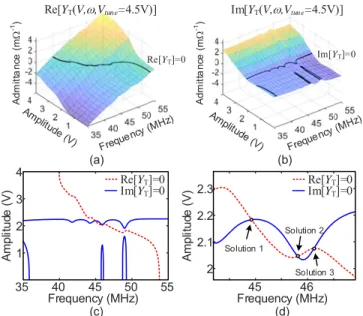
For each Vtune, the function YT in (18) is calculated versus the excitation amplitude V and frequency . The real and imaginary parts of YT provide two surfaces in the spaces V, , Re(YT) and V, , Im(YT), respectively [14]. As an example, Fig. 10(a) and Fig. 10(b) show the two surfaces obtained in the Colpitts oscillator for Vtune = 4.5 V, when considering a distance d = 22.5 mm between the oscillator and the board.
35 40 45 50 55 Frequency (MHz) Frequency (MHz)45 46 A m pl itu de ( V ) A m pl itu de ( V ) 1 2 3 4 2 2.1 2.2 2.3 (c) (d) Adm itt a nc e ( m -1) Im[YT]=0 Re[YT]=0 Im[YT(V,,Vtune=4.5V)] Re[YT(V,,Vtune=4.5V)] (a) (b) Adm itt a nc e ( m -1) Solution 1 Solution 2 Solution 3 Re[YT]=0 Im[YT]=0 Re[YT]=0 Im[YT]=0
Fig. 10 Contour intersection method. (a) Surface Re[YT(V,)] obtained for the
particular Vtune = 4.5 V and intersection with the plane Re(YT) = 0, providing
the contour r c
Y . (b) Surface Im[YT(V,)] and intersection with the plane Im(YT) = 0, providing the contours Y . (c) Intersection of the contours ci
r c Y
and i c
Y for Vtune = 4.5 V. (d) Expanded view about the region where the
contours r c Y and i
c
Y intersect. Three distinct solution points are obtained.
Then, one obtains the intersection of the surface Re[YT(V,)] with the plane Re(YT) = 0 and the intersection of the surface Im[YT(V,)] with the plane Im(YT) = 0 [13],[14]. For each Vtune, these intersections provide two contours, Ycr and i
c
Y , in the plane defined by V and , as shown in Fig.
10(a) and Fig. 10(b). The two contours r c
Y and Yci can be compactly defined as:
( ) , Re ( , , ) 0 r c tune T tune Y V contour V Y V V (19)
( ) , Im ( , , ) 0 i c tune T tune Y V contour V Y V V (20)For each Vtune, the solutions S V( tune) of the complex equation YT = 0 are the intersections of the two contours in (19) and (20), that is, ( ) r( ) i( )
Tune c tune c tune
S V Y V Y V . The intersections obtained for Vtune = 4.5 V are shown in Fig. 10(c) and Fig. 10(d). The latter presents an expanded view about the region where the two contours intersect.
Note that the method will be valid provided the oscillator waveform at the resonator node (RN) has a limited harmonic content, since it neglects the coupling effects at higher harmonic terms. This condition is valid for reasonably high-Q inductor. The same assumption is made in the experimental implementation of Section IV.
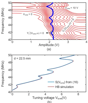
Vtune = 10 V 0 1 2 3 4 40 42 44 46 48 50 0 2 4 6 8
Tuning voltage Vtune(V)
40 42 44 46 48 50 F re q ue n cy (MH z) F re q ue n cy (MH z) Amplitude (V) (a) (b) Vtune = 0 Ycr(Vtune, = 0 HB simulation S(Vtune) from (16) d = 22.5 mm
Fig. 11. Oscillator analysis. (a) Intersections of the contours defined in (20) when varying Vtune. (b) Oscillation frequency versus the tuning voltage Vtune.
Solution curve resulting from these intersections compared with the one obtained through a HB analysis of the whole coupled system.
The whole solution curve is obtained by representing the distinct solution points (in terms of either V or ), obtained from the sequence of contour intersection, versus Vtune. Fig. 11(a) shows the contour intersections when varying Vtune. The contour r( )
c tune
Y V is nearly insensitive to Vtune whereas
( )
i c tune
Y V exhibits significant variations. For some Vtune values, in particular intervals, the contours r( )
c tune
Y V and i( ) 0 c tune
Y V intersect at three points (as in the case of Vtune = 4.5 V), which provides three steady-state solutions. In Fig. 11(b), the solution points obtained through the contour intersection of Fig. 11(a) have been represented in terms of versus Vtune. In
Fig. 11(b), the solution curve is compared with the one obtained through a HB analysis of the whole coupled system (with NH = 7 harmonic terms), with excellent results. The contour-intersection method enables a straightforward calculation of the oscillator solution curve under variations in any parameter affecting the electromagnetic simulation, since there is no need to recalculate ( , ,Y V Vtune).
Comparing Fig. 9 and Fig. 11(b), one obtains a good agreement between the resonances in Ycoup() and the three hysteresis cycles in Fig. 11(b). Actually, the observation of the hysteresis cycles is quite independent of the particular frequency characteristic of the oscillator circuit, due to the small coupling effects.
IV. EXPERIMENTAL CHARACTERIZATION OF THE HYSTERESIS CYCLES
A. Experimental apparatus
The experimental results presented here have been obtained from an updated version of the technique described in [15]. Specifically:
1. The previous work treated only the case in which the device under test (DUT) was a driven system; here, we have extended the idea to the case of an autonomous DUT (i.e., an oscillator).
2. An entirely new numerical method of path-following in
n-dimensional space has been implemented using simplicial decomposition [29],[30] which does not
require estimating a matrix of partial derivatives, hence is more suited to experimental work. A description of the implementation of a simplicial decomposition algorithm is provided in an appendix.
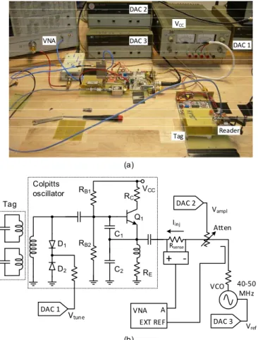
Fig. 12 shows the experimental apparatus and its block diagram, with the Colpitts oscillator (inside the dotted lines) implemented with a bipolar transistor as the autonomous DUT; the tuning voltage Vtune is generated by a digital-to-analog converter, DAC1. A signal is injected into the emitter of the Colpitts oscillator from an external VCO whose frequency is controlled by DAC3. The output of the injection source is buffered to prevent it being pulled by the DUT. This is an important practical point. The (buffered) output of the reference VCO is applied to the injection port of the DUT through a voltage-controlled attenuator driven by DAC2. Moreover, the injection current goes through a floating sense resistor (Rsense) connected to a differential active scope probe with a 50-Ohm output. A portion of the reference VCO output is applied to the reference port of an HP8753E network analyzer configured in "external source" mode. Finally, the output of the differential scope probe is applied to the A channel of the VNA, which functions as a phase-sensitive detector with large dynamic range.
C1 RE C2 RC RB1 RB2 Q1 D1
+ ‐
DAC 3 DAC 2 VNA A Vampl DAC 1 Vtune D2 Tag Colpitts oscillator Atten Iinj VCO 40‐50 MHz Vref EXT REF VCC Rsense (a) (b) DAC 1 DAC 2 DAC 3 VNA VCC Tag ReaderFig. 12. Experimental apparatus and system diagram; Three DACs are controlled by a computer which also interrogates the VNA over GPIB. The injection current (ideally zero) is measured across a series sense resistor with a high-impedance differential scope probe. The VNA serving as a sensitive null detector tracks the frequency of the reference VCO.
B. Numerical method
The entire measurement setup implements a mapping f from
R3 into R2. The input of this mapping is (Vtune, Vref, Vampl), which are, respectively, the tuning voltage of the DUT oscillator, the tuning voltage of the reference VCO and the control voltage for the amplitude modulator (a voltage controlled attenuator). The amplitude of the reference oscillator is fixed but the control voltage Vampl adjusts the amplitude of the injection signal to match the voltage waveform of the DUT. The output is Re(Iinj), Im(Iinj), where Iinj is the complex current circulating through the resistor
Rsense. The mapping f R: 3 R2 can be compactly expressed
as:
1 2
( , , ) Re( )
( , , ) Im( )
tune ref ampl inj
tune ref ampl inj
f V V V I
f V V V I
(21)
According to standard theory [29], the zero-set of this mapping – i.e., those triples x
Vtune,Vref,Vampl
that drive the real and imaginary parts of the injection current to zero – forms a one-dimensional manifold (a curve) in the three-dimensional space. The curve-tracking process starts with initial values for Vtune, the tuning voltage of the referenceVCO, Vref, and the amplitude setting of the reference VCO output Vampl to achieve a nulled current (in both real and imaginary parts); call this point x0. Then, a numerical
algorithm (to be described) advances along the zero-curve taking small steps in arc-length along the curve. In other words, arc-length is the quantity that advances monotonically during the tracing process. Particularly in the case of a fold-back or hysteresis response, any component of
Vtune,Vvco,Vam
x can go up or down during the trace, but
arc-length increases along the zero curve by construction. As described in the previous work [15], an application of an injection signal with nulled current does not change the state of the DUT, but can change its stability properties. In the case of an autonomous DUT, the frequency and phase of the oscillation of the DUT are determined by the reference oscillator (VCO) because the DUT injection-locks to it. In this sense, tracing a curve in the autonomous case is easier than in the driven case, because the phase of the injection signal does not need to be modulated during the tracing process. Fortunately, the signal at the emitter of the Colpitts (Fig. 12) is close to sinusoidal because of the high-Q tank inductor allowing the use of a sinusoidal VCO as the reference source. A more advanced implementation would attempt to synthesize a VCO waveform that is an exact match to the emitter waveform, possibly including higher harmonics. An alternative detector for the nulled injection current could probably be realized at VHF with a digitizing oscilloscope. The digital scope would be triggered from the VCO and the digitized waveform passed through a Fourier transform to extract real and imaginary parts at various harmonics.
A high-level description of an algorithm for tracing such zero-curves using simplicial decomposition is provided in Appendix A.
C. Experimental results
In Fig. 13, the simulation results are compared with the experimental measurements obtained when sweeping over the
Vtune range 0–10 V for a frequency sweep 40–50 MHz. The frequency exhibits hysteresis jumps because of the coupling to the passive tag resonators. The controlling computer sweeps monotonically Vtune in small steps up and then back down. At each step, the frequency of the Colpitts oscillator is monitored with a 500 probe on the collector of the transistor driving a counter with a General Purpose Interface Bus (GPIB). Qualitatively similar results can be obtained with a Colpitts circuit in which the tuning is accomplished by varying the value of a mechanical capacitor (which is linear at any fixed capacitor value) demonstrating that the hysteresis is not a non-linear effect introduced by the varactor.
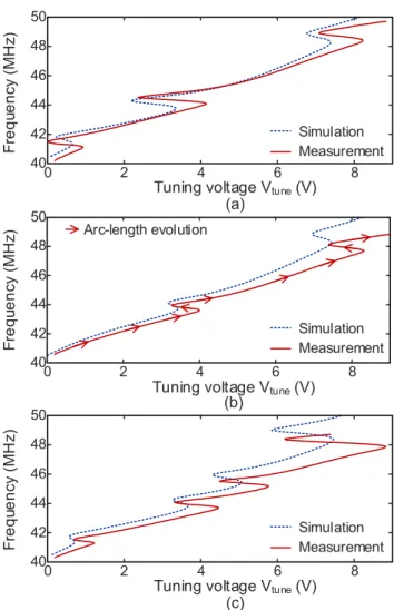
Fig. 14 shows experimental results using passive tags with different bit patterns, “1111” in (a), “0101” in (b) and “1101” in (c). The results are compared with simulations in the three cases. In Fig. 14(a) the same sweep used in Fig. 14(b) was repeated with the entire stabilization mechanism of Fig. 12, using the arc-length continuation algorithm. The resulting traces are shown in red and can, indeed, traverse the unstable portions of the hysteresis jumps.
As shown in Fig. 15, the measured stabilized and un-stabilized traces do not agree exactly (i.e., even in the physically stable portions of the curve). We attribute this discrepancy to a parasitic effect at the injection port which has not been completely nulled out. Another possibility concerns the voltage waveform at the emitter during the open-loop sweep. This waveform has clearly some second-harmonic content, approximately -17 dBc. As described above, a more sophisticated implementation would program an injection source to match both the fundamental and second harmonic (hence, nulling them) along the zero-curve. We are presently investigating such an improved implementation.
0 2 4 6 8
Tuning voltage Vtune (V)
40 42 44 46 48 50 F re que nc y ( M H z) Simulation Measurement
Fig. 13. Comparison of the simulation results with experimental measurements; a controlling computer applied a monotonic sweep up and sweep down to a DAC to generate Vtune, then interrogated a frequency counter connected to the collector node of the oscillator. For this graphic, Vtune is
swept up [0,10] then down [10,0] V to generate the hysteresis steps.
V. READING THE TAG
Several methods of reading the tag have been considered and implemented. A simple technique would apply a stepped voltage ramp waveform as the tuning voltage of the VCO and measure the oscillator frequency at each voltage step. The reader would ramp up and down over the same tuning range and look for an obvious frequency difference at the frequencies assigned to bit positions of the tag for the ramp-up versus ramp-down sweep. A significant frequency difference would encode a "1" bit and little or no frequency shift would encode a "0" bit. The ramp-up and ramp-down frequency measurements for a "0" bit might be slightly different due to noise, but nowhere near as large as when the passive tag resonator induces hysteresis at the bit frequency. The experimental results presented here have been obtained with such a scheme using an HP5386 counter connected to a computer over GPIB. This scheme seems implementable in a portable tag reader, but would require a micro-processor control and a reasonably accurate frequency counter operating at the VCO frequency. This might be too expensive for some applications.
0 2 4 6 8
Tuning voltage Vtune (V)
40 42 44 46 48 50 Fr e q ue n cy ( M H z) Simulation Measurement (a) 0 2 4 6 8
Tuning voltage Vtune (V)
40 42 44 46 48 50 Fr e q ue n cy ( M H z) Simulation Measurement (c) 0 2 4 6 8
Tuning voltage Vtune (V)
40 42 44 46 48 50 F req ue nc y ( M H z) Simulation Measurement (b) Arc-length evolution
Fig. 14. Comparison between the experimental and simulation results obtained when using passive tags with different bit patterns, “1111” in (a), “0101” in (b) and “1101” in (c). For this graphic, the experimental apparatus increases arc-length along the curve monotonically; Vtune can go in either direction
during the arc-length sweep.Arc-length is set to 0 at the lower left-hand point of the curve, and increases to a final value at the upper-right hand end. The actual value of the final length depends on scaling. Arrows showing arc-length evolution have been included in (b).
0 2 4 6 8
Tuning voltage Vtune (V)
40 42 44 46 48 F requ enc y ( M Hz )
Unstabilized measured curve Stabilized measured curve
Fig. 15. Measurements of the stabilized (solid line) versus un-stabilized (dashed line) sweeps of the same passive tag.
We have implemented an alternative technique employing dual oscillators as shown in Fig. 16. The tuning voltages of two VCOs are driven from the same sawtooth waveform. The oscillators track but with a deliberate offset in frequency as
shown in Fig. 17. The offset is necessary to prevent the two oscillators to injection-lock to each other when coupled through the mixer.
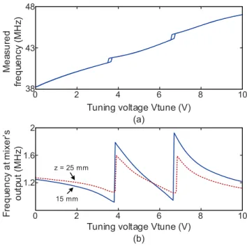
Oscillator 1 in Fig. 16 will be coupled to the tag resonators while oscillator 2 is designed to have very little coupling. For example oscillator 2 could use a toroidal inductor which is self-shielding. A mixer and low-pass filter are then used to extract the difference in frequency between the two oscillators as a function of the common tuning voltage.
Tag LPF Sawtooth Osc 1 Osc 2 Frequency to voltage
Fig. 16. Inexpensive tag reader employing two oscillators. The oscillators track in frequency, but with a deliberate offset to avoid injection-locking. The tag resonances generate jumps in the difference frequency which can be detected by a low-frequency analog circuit. As shown in Table I, a typical sensitivity for such a circuit would be 1 V/MHz, resulting in a very distinct read signal.
In the absence of a tag, this frequency difference is close to a constant value. Our present implementation uses an analog linearizer network to achieve some improvement in linearity between the tuning voltage and frequency of the VCO but it is a very simple circuit. A more sophisticated implementation should be able to get the two traces of Fig. 17 very nearly straight and parallel. However, when a tag is coupled to oscillator 1 there are distinct jumps in the frequency difference corresponding to "1" bits in the tag. Fig. 18 shows a read of the bit pattern "0101" at distances of 1.5 cm and 2.5 cm. The present implementation measures the frequency difference with a counter but -- considering that the difference frequency is small compared to the tuning frequencies – it should be possible to use an analog frequency-to-voltage converter [31] to generate a DC voltage proportional to the frequency difference for each tuning voltage. Such circuits are simple and have a fast response allowing for a small period to the sawtooth signal. Table I presents our implementation of the RFID system is based on the principle described in [22], where the impedance of the tag influences the frequency of a sweep-tuned oscillator, acting as a reader.
Finally, a more sophisticated method would actually perform a stabilized sweep with a path-following algorithm. This computation should be within the capabilities of a modern microprocessor. If such an algorithm could be implemented in the tag reader, we believe it would provide a robust read process and also allow the bit frequencies of the tag to be more closely spaced, possibly even with overlapping hysteresis loops. The reader would deduce the encoded bit pattern from the tag by looking for the presence or absence of
a pair of turning points in the path bracketing a bit-encoding frequency.
Our present laboratory implementation of the stabilized sweep is slow because a network analyzer is used as a coherent detector for the null current. There is also some time spent in transferring the data from the network analyzer to the computer implementing the path-following algorithm. However, we do not believe these limitations to be fundamental to the method and an implementation allowing faster stabilized sweep is under study. Observe that with a stabilized sweep, complete information is obtained with only one sweep direction.
0 2 4 6 8 10
Tuning voltage Vtune (V)
35 40 45 50 F re q ue n cy (MH z) Osc. 2 Osc. 1
Fig. 17. Experimental frequency tracking of two VCOs with deliberate offset.
z = 25 mm
15 mm
0 2 4 6 8 10
Tuning voltage Vtune (V)
38 43 48
(a)
0 2 4 6 8 10
Tuning voltage Vtune (V)
1.2 1.6 2 (b) F re q ue n cy a t mi xe r’s ou tp u t ( M H z) Me as u re d fr e q ue n cy (MH z)
Fig. 18. Tag reading using the setup employing two oscillators shown in Fig. 16. (a) Frequency characteristic when oscillator 1 is coupled to a tag with two enabled resonances. (b) Mixer output. The figure shows a read of the bit pattern "0101" at distances of 15mm, and 25 mm.
Table I compares our approach with a recent alternative [22] for reading a passive RFID tag, also based on sensing the response of an oscillator coupled to the tag. Because the two approaches use very different frequency ranges, it is difficult to give a side-by-side comparison. Our approach is probably a bit more expensive to implement in the tag reader, but does
give a much more distinct signal for the individual bits encoded by the passive tag.
TABLE I
COMPARISON WITH PREVIOUS RESULTS USING A SWEEP-TUNED OSCILLATOR
Criterion [22] Present work
Frequency range 2.4-3.4 GHz 40-50 MHz
# Bits 10 4
Tag size 25 x 40 cm 50 x 50 cm
Read method DC bias change Output of F/V converter Delta V per bit < 1 mV > 500 mV* Estimated reader cost 1 Eur 2 Eur * Using frequency-to-voltage converter with sensitivity of 1 V/MHz
The theoretical analysis presented here has assumed that there is no coupling between individual resonators of the tag itself – only tag-to-oscillator coupling has been treated. In practice, we have observed some coupling between adjacent tag resonators as a second-order effect. Enabling or disabling an encoding bit causes a slight shift in the resonant frequency of adjacent spiral resonators, due to (weak) side-to-side coupling. Again, we do not see this as a fundamental impediment in practice. A passive tag encodes a fixed bit pattern, and a computer optimization could be used to tweak the resonator values to compensate for coupling between adjacent spirals.
VI. CONCLUSIONS
A method for the analysis and synthesis of multiple hysteresis loops in the frequency-tuning curve of an oscillator coupled to a number of external resonators has been presented. The equivalent coupling admittance seen from the core-oscillator terminals has been derived and its particular form of variation has been explained in detail. From the analysis of this function, conditions to avoid the overlapping of hysteresis cycles in the oscillator tuning curve have been derived. A possible application of coupling induced hysteresis in chipless RFID, using an oscillator as a compact reader, has been explored. This application would take advantage of the vertical frequency jumps (associated with the hysteresis phenomenon) to increase the sensitivity to the tag resonances. A proof of concept based on a Colpitts oscillator, with the coupled inductors implemented through planar spirals, has been presented. The coupled system is analyzed extracting the nonlinear admittance function of the core-oscillator, in addition to the coupled admittance, calculated through an electromagnetic simulation. A new numerical method for the experimental characterization of the hysteresis loops, able to pass through their unstable sections, has also been presented, including the mathematical algorithm and the detailed experimental set-up. This should enable an improvement of the shape the hysteresis cycles for an optimum incorporation into the RFID system.
ACKNOWLEDGMENT
R.M. would like to thank Thomas Banwell (Perspecta Labs), Andrew Stillinger (New Jersey Institute of Technology), Michael Henderson (IBM Watson Research) and Ken Bond (MetroWest Technologies).
Appendix A
This section gives a high-level description of an algorithm for tracing a one-dimensional curve.
Zero‐Curve Arc‐length x0 0 1 Vtune Vam pl
Fig. 19. Geometry of path-following algorithm. The zero-curve, starting from
x0 and advancing in arc-length, has crossed from simplex 0 into simplex 1 across the facet common to both simplices. The method to identify such transversal facets is described in the text.
Fig. 19 indicates the geometry involved in such a simplicial path-following algorithm. Our previous implementation of a path-following algorithm [15] required a Jacobian matrix of partial derivatives approximated by finite-differencing, which was slow and somewhat noisy. The use here of simplicial methods (which do not require a Jacobian matrix) seems much better suited to experimental work. Starting at the initial point
0
x described above, the algorithm attempts to follow said zero
curve until a specific arc-length goal is reached. The user chooses an arc-length goal large enough to include interesting features in the zero curve such as a hysteresis fold-back.
The algorithm constructs a tetrahedron 0, centered on x0
with size determined by a user-supplied parameter “grain”. For tuning and control voltages in the range [0,10], a typical grain value might be 0.05. A small grain value gives fidelity along the curve, but at some point goes below the resolution of the various DACs. In three-dimensional space a tetrahedron is a simplex – roughly speaking the simplest object that has volume [32],[33]. A simplex in n-dimensional space is determined by n+1 points that do not lie in any sub-space of lower dimension. For example, four co-planer points in R3 would violate this condition and not qualify as a simplex. The tetrahedron above has four faces determined by any combination of three vertices. In the general case of a simplex, such faces are called facets.
The supporting theory [29] shows that a simplex typically intersects the zero curve in two facets of the simplex or not at all. In other words, moving along the zero curve in the sense of increasing arc-length, the zero curve enters a simplex through one facet and exits it through a different facet. In the supporting literature this is sometimes called the "in door, out door" principle. If the zero curve enters and exits a simplex more than one time, then the simplex is too big. Degenerate cases in which the zero curve intersects an edge or vertex of a simplex are treated in the literature [30] but can largely be ignored in practice because they are so rare.