Device Physics of Hybrid Perovskite Solar cells: Theory and Experiment
98
0
0
Texto completo
(2) Perovskite solar cells exhibit a series of distinctive features in their optoelectronic response that have a crucial influence on the performance, particularly for long-time response. Here, a survey of recent advances both in device simulation and optoelectronic and photovoltaic responses are provided, with the aim of comprehensively covering recent advances. Device simulations are included with clarifying discussions about the implications of classical driftdiffusion modeling and the inclusion of ionic charged layers near the outer carrier selective contacts. The outcomes of several transient techniques are summarized, along with the discussion of impedance and capacitive responses upon variation of bias voltage and irradiance level. In relation to the capacitive response, a discussion on the J V curve hysteresis is also included. Although alternative models and explanations are included in our discussion, the review relies upon a key mechanism able to yield most of the rich experimental responses. Particularly for state-of-the-art solar cells exhibiting efficiencies around or exceeding 20%, outer interfaces play a determining role on the PSC´s performance. The ionic and electronic kinetics in the vicinity of the interfaces, coupled to surface recombination and carrier extraction mechanisms, should be carefully explored to progress further in performance enhancement.. 2.
(3) Article content Device Physics of Hybrid Perovskite Solar cells: Theory and Experiment 1.. Introduction 5. 2.. Structure of perovskite solar cells. 3.. Numerical simulation of perovskite solar cell devices. 4.. 5.. 6.. 8 11. 3.1.. Effect of ionic species on the electric field of PSCs 18. 3.2.. Effect of the type of semiconductor conductivity. 3.3.. Dipolar distribution of ions 22. 3.4.. Comparison of the DD and the dipolar distribution of ions 24. Transient response measurements. 21. 27. 4.1.. Characteristic response times and basic transient behavior 27. 4.2.. Slower than seconds relaxation processes. 35. Impedance and capacitance features of perovskite solar cell devices 5.1.. Definitions. 5.2.. Dark capacitance and dielectric components 47. 5.3.. Capacitance from light induced transients. 5.4.. The low frequency capacitance under steady state illumination. 5.5.. Negative capacitance and the equivalent circuit. 52. 60. Dark J-V curve hysteresis. 6.2.. Capacitive hysteresis and step voltage scans under illumination. 6.3.. Effect of pre-conditioning on J-V curves. 6.4.. Hysteresis interpretation: two main models 72. 6.5.. Inverted hysteresis and non-capacitive currents. 6.6.. Other factors affecting hysteresis and its suppression. 8.. Acknowledgments. 9.. References. 54. 56. 6.1.. Conclusions 88. 39. 40. Current-voltage curve hysteresis. 7.. 1. 62. 88. 89. 3. 68 78 81. 65.
(4) Osbel Almora graduated in Physics from the University of Havana, Cuba, in 2013 and joined the Institute of Advanced Materials of the Universitat Jaume I of Castelló, Spain in 2014. His main topic of interest is the characterization and modeling of energy devices. Most of his research activities have been focused on all-solid-state photovoltaics, including CdTe, perovskite and silicon solar cells.. Juan Bisquert is a professor of applied physics at Universitat Jaume I de Castelló, and the Director of the Institute of Advanced Materials. He has developed the application of measurement techniques and physical modeling that relate the device operation with the elementary steps that take place in the materials and interfaces. He authored a series of books including Nanostructured Energy Devices (1. Equilibrium Concepts and Kinetics, 2. Foundations of Carrier Transport) and 3. Physics of Solar Cells: Perovskites, Organics, and Photovoltaics Fundamentals (CRC Press).. His current main. research interests are perovskite solar cells and solar fuel production.. 4.
(5) 1. Introduction Despite the significant advances in power conversion efficiency (PCE), several issues on the characteristic phenomenology of perovskite solar cells (PSCs) are still poorly understood. Among these, one can highlight the diverse time (t) domains of different processes, the corresponding dynamic evolution of charge distributions and the consequent current densityvoltage ( J V ) curves. About the latter, significant debate has taken place on the anomalous hysteresis phenomenon that currently generates some doubts on the actual PCE reports. The main argument here is that for PSCs, the achievement of a well-defined steady state is quite difficult, thus for instance the definition of a reliable short-circuit current density ( J sc ) or open-circuit voltage ( Voc ) can be problematic in some cases. Accordingly, typical charge extraction evaluation at short-circuit (SC) or the determination of recombination at opencircuit (OC) are also not so evident. The study of high efficiency PSCs is accompanied with the analysis of the fundamental physico-chemical mechanisms underpinning their performance. Perovskite solar cells exhibit dynamic hysteresis in their J V curves[1-3] strongly dependent on the voltage scan rate, direction (from positive to negative bias, or the opposite way), the bias point before a scan, and pre-conditioning treatments (in darkness, or under illumination at open-circuit or shortcircuit).[4, 5] They also show a low-frequency giant capacitance response[6, 7] and anomalous experimental transient results,[8,. 9]. not observed in classical solar cells. Different possible. origins of these phenomena have been proposed: trapping of electrons and holes,[10, 11] mobile ions in the perovskite film[12,. 13]. and chemical or structural changes in the material.[5,. 14]. Recently, the slow changes associated with the dynamic hysteresis in PSCs have been attributed to the redistribution of slowly moving ions.[1,. 6, 15-17]. The atomistic study of the. motion of the different particles involved in the internal dynamic of the perovskite (electrons, holes, molecules, ions) also supports this statement.[18] The nature and time scales of these different motions have been quantified with the combination of first-principle and multiscale 5.
(6) material modeling and experimental techniques, such as neutron diffraction measurements, quasi-elastic neutron scattering, and ultrafast vibrational spectroscopy.[18] Different theoretical models and experimental settings assist the interpretation of the effects of ion migration. Macroscopic studies include the analysis of the conductivity, the modeling of dynamic hysteresis[2, 3, 19] or temporal experimental settings such as photovoltage decays[8] or chronophotoamperometry.[6, 9] The type of microscopic mechanisms that intervene in the migration, such as vacancy assisted migration or movement by interstitial ions/defects, and the particular details of their transport through the perovskite are particular topics of study.[20, 21] These studies include the determination of the activation energies for these migration mechanisms using density functional theory,[21] and are compared with kinetic data extracted from the current-voltage response of PSCs.[6] Also, the direct determination of the ion diffusion coefficient has been recently addressed.[22] High-computational studies involving electronic structure, molecular dynamics, and Monte Carlo simulation[20] shed light on the chemical bonding of hybrid perovskites. The peculiar phenomena that turn out to be ubiquitous in perovskite solar cells make it necessary to adopt a fresh view on physical modeling and measurement that we attempt to summarize in this review paper. Many of the well-established tools and techniques come into question, and specific intuition about central features such as band bending need to be reevaluated. Here we present a first systematic effort to provide a unified picture of the physical modeling and measurement that has been gathered from the initial years of study of the field. Our analysis is far from complete as we believe that the study still needs years of work ahead, and the definite research directions will depend markedly on the ways that materials development of the perovskite solar cell occurs. However, the present work provides a general guideline of studies that were absent in the first years of the perovskite solar cell studies, causing great confusion about the interpretation of physical measurement. We begin the study with a summary description of the structure, materials, configurations and operation of the perovskite solar cells. These topics are broadly covered in a variety of 6.
(7) review papers and monographies that the reader may consult if more general information is needed. In Section 3, we present a detailed analysis of the physical effects of mobile ions in the solar cell properties. In normal solar cells, it is implicitly assumed that ions form a background fixed charge density, determining the minority carrier. However, new physical effects happen when several types of ions can slowly flow within the device. The notion of doping becomes problematic, the interfaces can experience strong accumulation effects, and the issue needs a careful discussion by simulation that we have explained by separating many cases in order to provide physically based intuition about the energy diagram for interpreting a wide variety of experimental situations. After exploring the variety of steady-state band diagrams from simulations tools, we summarize in Section 4 the rich phenomenology observed from experimental transient responses. Contrary to that occurring for other photovoltaic technologies, it is clearly stated for PSCs that operating mechanisms spread in time from ns up to tens or hundreds of seconds. While PL transients exhibit rapid decays for the radiative recombination process in the nanoseconds time scale, voltage or current transients present distinct trends with multiexponential decays. Particularly illustrative is the dependence of the voltage decay in open circuit on light-soaking time. The long-time response, in the domain of seconds, is fully altered by the pretreatment signaling the occurrence of dynamically slow ion polarization at the contacts in connection to the charge recombination. In Section 5, a survey on experimentally gathered impedance and capacitance data is provided. The most intriguing observation, in relation to the solar cell functioning, is the commonly reported light- and voltage-dependent huge values of the low-frequency capacitance (surface capacitance). Its frequency range of observation (seconds) points to the slow transient phenomena treated in Section 4. Again, this is a distinctive feature of PSCs rarely distinguishable in other solar technologies. Dependences of the surface capacitance on perovskite layer thickness and irradiance level allows connecting it to specific ionic or electronic accumulation mechanism at the outer interfaces. 7.
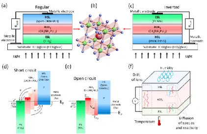
(8) Finally, the issue of the J V curve hysteresis is extensively addressed in Section 6. This topic attracts continued interest, due both to the significance of this phenomenon for practical operation of the solar cell, and to the variety of phenomena that may act for the delayed and variable response. A summary of the phenomenology on hysteresis and classification of the responses is provided in relation to the variation in control parameters such as scan rate, scan step, temperature, pre-biasing and light soaking. Models for hysteresis are explained stressing the consistency of the ionic/electronic charge accumulation at the electrodes (surface polarization model) with the observed responses and impedance analysis. Strategies of hysteresis suppression are also commented upon. We finish with a few remarking conclusions.. 2. Structure of perovskite solar cells PSCs are basically structured as a light harvesting perovskite sandwiched between the electron and hole selective layers. The use of numerous materials has been reported,[23] however the most successful and extensively studied configuration is that shown in Figure 1a, where the TiO2 layer is grown on top of the fluorine-doped tin oxide (FTO)/glass substrate (typically as a mesoporous scaffold on top of a compact layer), then the methylammonium lead iodide CH3NH3PbI3 (referred as MAPbI3 in the next) perovskite and subsequently the spiro-OMeTAD. (2,2‟(7,7‟)-tetrakis-(N,N-di-p-methoxyphenyl-amine)9,9‟-spirobifluorene).. The metallic electrodes are often made of gold in order to achieve better connections with the load (RLoad), even though other non-precious metals have been also explored.[24] Thus, in this regular structure, the light crosses the substrate through the glass and the transparent conducting oxide (TCO), then first through the electron-selective layer (ESL) to be absorbed at the perovskite, leaving the hole-selective layer (HSL) at the end of the light path.. 8.
(9) Figure 1. Basic structure of PSCs in (a) regular and (c) inverted configurations. (b) Crystalline structure of perovskite materials in cubic phase ABX3, where A, B and X are CH3NH3+, Pb2+ and I-, respectively, for CH3NH3PbI3. General energy band diagram in SC (d) and OC (e) for different possible perovskite conductivities, as indicated, being E F the equilibrium Fermi lever and E Fn and EFp the quasi Fermi Levels for electrons and holes, respectively. (f) Main contributing factors in the degradation processes of PSCs. Most used materials in each case are specified in parenthesis. Adapted with permission.[25] Copyright 2017, Sociedad Cubana de Física.. Another important configuration is that of Figure 1c, known as an inverted structure. Here, in. the. same. light. path. direction,. the. sequence. of. layers. is. glass/TCO/HSL/perovskite/ESL/metallic-electrode.[26] The selective contacts for these devices are mainly fullerene derivatives and organic compounds, with PCBM ([6,6]-phenyl-C-61butyric acid methyl ester) and PEDOT:PSS (poly(3,4-ethylenedioxythiophene) doped with poly(4-styrenesulfonate)) being the most common ESL and HSL, respectively. However, irrespective of one or other configuration, MAPbI3 has proved to be the most representative perovskite for photovoltaic applications. As systematically described by Stoumpos et al.,[27] in its high temperature cubic phase, the methyl ammonium organic cation CH3NH3+ (MA) is A in the perovskite general formula while the lead and the halogen are B 9.
(10) and X, respectively, with the crystalline structure that of Figure 1b. Remarkably, MAPbI3 has an optimum direct band-gap ( Eg 1.6 eV )[27-30] and the deposition of the material follows easy solution-based fabrication processes, e.g. dip and spin coating,[31, 32] resulting in layers with good crystalline quality at relatively high reaction rates, even when processed at low temperatures. The estimated theoretical PCE for a 500 nm-thick MAPbI3-based single junction solar cell has been calculated to be around 31% with J sc 26 mA cm-2 , Voc 1.3 V and 91% of fill factor (FF).[33] Importantly, the electrical intrinsic conductivity of MAPbI3 can be modified from p-type to n-type by controlling growth conditions, i.e. by managing the concentration of donor or acceptor shallow defects.[34] For example, recent studies have shown that exposure to excess I2 vapor pressure can create intrinsic p-type conduction in MAPbI3.[35,. 36]. This tunable. conductivity character has produced a significant scattering in the representation of the energy band diagram of PSCs. While several studies have identified or assumed an intrinsic character of the perovskite, meaning a p-i-n heterojunction, some others suggest p+-p-n or p-n-n+ heterojunctions.[25] The two possible energy band diagram situations are illustrated in Figure 1d at short-circuit (SC) and in Figure 1e for open-circuit (OC) condition. It seems that not gross differences are expected at OC, however at SC, the photocurrent generation is quite sensitive to the nature of minority carriers. Regarding these issues, and including the effects of ions, a more detailed discussion from theoretical modeling by numerical simulations can be found in Section 3.1 to 3.3. Concerning the general performance, the two other most characteristic perovskites are the hybrid halide CH3NH3PbI3-xClx. and the formamidinium (FA) cation composed. HC(NH2)2PbI3.[37] About the former, the chlorine incorporation has been found to mainly improve the carrier transfer across the heterojunction interfaces[38] while in FAPbI3 based devices, a broader absorption toward the infrared region[39] has been obtained. In addition, one weighty consequence of the PSC structure and involved materials is the 10.
(11) occurrence of significant degradation processes. Despite degradation not being the focus of this review, we briefly mention some important points about this issue in order to support subsequent considerations along the varied discussed phenomena where the reactivity influence cannot be ignored. In Section 5.2 and 6.5, the impact of reactivity mechanisms on capacitance and J V curves will be noted explicitly. These mechanisms are summarized in Figure 1f, with the moisture being the first to be highlighted. MAPbI3 degradation in humid air proceeds by two competing reactions: (i) the generation of a MAPbI3 hydrate phase by H2O incorporation and (ii) the PbI2 formation by the desorption of CH3NH3I species.[40] Subsequently, loss of CH3NH3+ and I- species and decomposition into PbCO3, Pb(OH)2, and PbO take place.[41] Even if the material is properly encapsulated (or measured in lab conditions under inert atmosphere), devices can still be unstable. Particularly, it has been shown that ionic transport induced by the electrical field can lead to the chemical reactivity of the external contacts with iodide ions.[42,. 43]. In addition, the temperature can induce. decomposition at local temperatures around 100ºC and phase transitions around 57ºC. This is a catalytic factor for the other degradation processes.. 3. Numerical simulation of perovskite solar cell devices Experimental evidence and theoretical models for simultaneous electron and ion transport in the hybrid perovskite materials show that PSCs exhibit characteristics of mixed ionicelectronic conduction. Electronic conduction is quite common and necessary in photovoltaic materials, but facile ion transport by hopping between favorable lattice sites is a less usual characteristic that appears unexpectedly.[44] This effect causes an enormous impact on the understanding of the PSC device operation, as it implies that general properties like the internal band bending, electric field distribution, and carrier injection characteristics at the boundaries with the contacts can have a dynamic change over different timescales under operation. Then, characteristics that are taken for granted in other well-known semiconductor 11.
(12) devices are seen to vary and fluctuate in the PSC. This fact poses a major barrier for understanding and control, as for example, results of many techniques are not reliable, since they depend on details of the measurement protocol. Different distributions of ions inside the perovskite film can alter the electronic operation when illuminated by sunlight. This fact has important implications in terms of the long-term stability[6] as well as the efficiency of the solar cell.[45] For this reason, we begin the review with an analysis of the solar cell device characteristics taking into account the variations caused by the massive displacement of ions. In perovskite materials, the mobile ionic species are associated with vacancies, ions or interstitial defects.[6] Density function theory (DFT) studies at room temperature on MAPbI3 show the existence of high concentrations of iodide vacancies and methylammonium (MA) vacancies.[46] Some first-principle studies in MAPbI3 perovskites have shown that the most diffusive species (higher mobility) is the I- anion,[6, 47] and suggest the requirement of a long period of time for the migration of Pb and MA vacancies. This was further supported by theoretical calculations[48,. 49]. that identified Iodide vacancies as the defect with the lowest. formation energy (~0.67 eV) in MAPbI3 similar to values reported by Eames et al.[6]. However, other experimental studies have confirmed the motion of MA+,[50] with some authors even claiming migration of both I- and MA+ ions.[51] Some studies on MAPbI3 suggest an important equilibrium concentration of iodide (I-), lead (Pb2+) and CH3NH3+ (also denoted as MA+) vacancies, with their respective ions of opposite charge. Other migrating species such as gold[52] or hydrogen[53] have also been detected in perovskite semiconductors. Therefore, it has been difficult to identify which ions contribute to the strong ionic conductivity observed. However, recent experiments on ionic conduction in perovskites by Senocrate et al.[35] have shed new light on this issue. They first identified that the I- ion is the dominant long range mobile ionic species (as also corroborated by Li et al.[54] from wide-field PL imaging microscopy) in the perovskite by passing a small current (nA) for one week through a Faradaic cell of type +Cu/MAPbI3/AgI/Ag-, while subsequent XRD measurements showed the only phase change that occurred was the formation of CuI at the Cu/MaPbI3 side. 12.
(13) In addition, they determined no long range diffusion of MA+ ions, through a similar measurement on a +Pb/MAPbI3/AgI/Ag- cell and tracer diffusion experiments on 13C and 15N enriched MAPbI3 pellets in contact with each other. The authors then measured the evolution of voltage in a dc galvanostatic configuration of a pure MAPbI3 pellet while varying the I2 partial pressure, allowing for the estimation of the values of ionic and electronic conductivity over a range of partial pressure values. They found that the ionic conductivity reduced with increasing I2 partial pressure, related to the filling of Iodide vacancies, hence establishing Iodide vacancy migration as the primary mechanism of ionic movement through the perovskite. However, as a generalization, for the steady state analysis, we consider only two ionic species, cations and anions, and assume neutrality of ionic charge in the perovskite as a whole. Currently, there are two main factors that make ion migration alter the solar cell performance. These two effects will have a protagonist role along our paper, since they will be used for the interpretation of hysteresis in the final part of the paper. First, the internal electric field created by any biasing voltage, or by the effect of lightinduced photovoltage, produces accumulation of ions at the interface contacts.[8] This charge accumulation has a very strong effect on the measured surface capacitance,[55, 56] which is seen to change dramatically depending on the contact material. [2, 57] [58, 59]. . This mechanism may. have a major impact on degradation of the contacts[42] (highlighted in Figure 1f). This is because, on the one hand, mobile ions inside the perovskite structure show a very slow motion that progressively adjusts to the variations of voltage. This fact points out a severe influence of the surface polarization on the observed slow dynamic changes in measurement. In addition, the ions accumulated at the interfaces may launch slow electrochemical reactions and even penetrate selective contact material producing severe degradation.[42] The second effect associated with ion migration refers to the influence of the electrical field distribution on charge collection. In a perovskite solar cell, a large built-in voltage could be expected, and this original voltage can be modulated by the ion drift, modifying the charge 13.
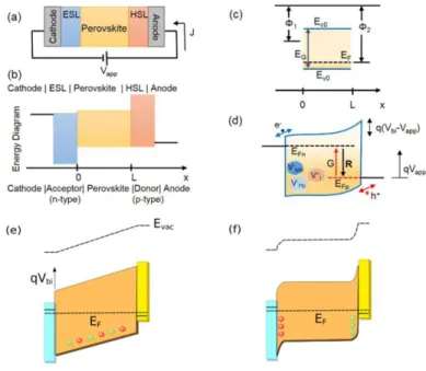
(14) collection properties,[5, 6, 9, 19] see Figure 2. Therefore, the internal electrical field is screened by the ion distribution and the net electric field modifies the value of the photocurrent. In order to quantify these effects, one needs to address the complex problem of device simulation considering not only usual models combining electrons and holes but additional anionic and cationic species that can be redistributed inside the absorber layer. We will provide a short account of the methods used to deal with these problems and then we present and discuss the most relevant problems based on a specific solution model. Accurate modelling and device simulations present significant challenges for describing the mixed ionic-electronic conduction. A well-known simulation tool that supports macroscopic studies in PSCs is drift-diffusion (DD) simulation.[19,. 47, 60]. Nevertheless, not all the DD. simulations model the distribution of ions in the same way.[61] DD simulation is usually applied to structures such as the one shown in Figure 2a-b or the simplified structure of Figure 2c. In these figures, the cathode in contact with the electron selective (hole blocking) layer (ESL) and anode close to the hole selective (electron blocking) layer (HSL) are highlighted. Furthermore, the distance x from the ESL/perovskite interface is indicated, which will be x L at the HSL/perovskite interface for our purposes.. Figure 2.. (a) Layers of the PSC: cathode-ESL-perovskite-HSL-anode. (b) Energy diagram. of the different layers before contacting. (c) Simplified energy diagram of a p-type solar cell 14.
(15) before contacting in which the effect of the ESL and HSL is incorporated as boundary conditions. (d) Energy diagram for the solar cell under bias voltage Vapp. Only electrons and holes contribute to the electrical current. (e) Energy diagram of intrinsic perovskite with a built-in potential as shown, establishing an electrical field through the perovskite that is the difference in work functions between the ESL and HSL. The ions (cations and anions are green and red respectively) drift along this electrical field and establish the equilibrium situation of (f), where the shielding of the electrical field through the bulk occurs. Adapted with permission.[3] Copyright 2017, Royal Society of Chemistry.. Some DD simulations consider a steady state ion distribution produced by drift-diffusion mechanisms inside the perovskite, and ion blocking contacts at the perovskite boundaries.[4, 19, 47, 62]. In this approach, the drift and diffusion of anions and cations is coupled with the well-. known drift-diffusion model for electrons and holes.[8, 19, 47] It is worth mentioning the models proposed by Van Reenen et al.,[62] Richardson et al.,[19] O‟Kane et al.,[4] Calado et al.,[47] Gottesman et al.[8] and Neukom et al..[63] Their main differences lie in their approaches of the boundary conditions and the inclusion of different physical-chemical mechanisms in their models. In order to obtain quick simulation approaches, the use of approximate distributions of anions and cations is common practice.[4,. 9, 19]. Some authors propose that under a net. electric field inside the perovskite (Vbi Vapp ) / L 0 ( Vbi is the built-in voltage, given by the difference of contact work-functions, and Vapp is the external voltage applied between anode and cathode) the positively charge ion vacancies drive into the region of the perovskite adjacent to the HSL. There, they create a narrow positively charge layer. To maintain the neutrality, a negatively charge layer appears, by depletion of the positive vacancies, in the perovskite near the ESL. These regions of opposite charge are termed Debye layers[4, 19, 60, 64] and resemble a dipolar distribution of charge in which the positive and negative charges are confined in thin layers close to the interfaces,[9, 65] with ionic Debye length[64] 15.
(16) LD . r 0 kBT q2 N. ,. (1). where r and 0 are the relative and vacuum permittivity, k B is the Boltzmann constant, T the temperature, q the elementary charge and N is the total density of mobile ions forming the interfacial space charge of the diffuse layer. The band energy structure of the perovskite semiconductor, as seen by charge carriers, is modified electrostatically by the Debye layers, which act to screen the built-in field.[4] At high ion densities, the Debye length is over two orders of magnitude smaller than the perovskite width (a few nm compared to hundreds of nm). The inclusion of these thin layers in simulations represents a computational challenge. For this reason, Richardson et al.[19] and O‟Kane et al.[4] provided a model that adds asymptotic expressions for the charge in the Debye layers to the DD simulations. In this model, exponential voltage drops are associated with the Debye layers, and a constant compensated electric field is assumed in the bulk between these layers. This model needs further discussion, concerning the important feature of charge accumulation at contact interfaces that explains the giant capacitance as described later. Other DD simulations incorporate qualitative models, including schematic energy diagrams for the distribution of the compensated electric field in the bulk after the migration of ion vacancies.[6, 9, 66] Authors expect the magnitude of the J sc to be controlled by the extent to which the electric field is screened.[5, 6] Tress et al.[5] solved the DD equations modifying the built-in voltage in relation to the electric field compensation amount in the bulk. They suggested that the rate-dependent hysteresis observed in J-V scans is related to a slow fieldinduced process that tend to reduce the electric field in the device at each applied voltage, and thus, modify the charge collection efficiencies.[5] In a similar way, Zhang et al.[66] also proposed that the presence of these ions at the interface attracts charge that modifies the energy-band bending. This interface charge affects the value of the photocurrent. In that work, Zhang et al.[66] suggested that the lower the interface charge density, the higher the obtained photocurrent. The aforementioned mechanism suggests that the dynamic change in the 16.
(17) interface charge leads to J-V hysteresis. Despite these efforts, a precise quantification of the screening of the electric field in the bulk of the perovskite is lacking. In this regard, we proposed a numerical simulation of a perovskite structure in which mobile ions are present, as further described below.[61] Another topic under study concerning the ion migration is related to the specific ions that are transported through the perovskite (a further analysis is provided in Section 3.1). Richardson et al.[19] and Calado et al.[47] distinguished between slow ions with a uniform concentration along the perovskite and fast ions that are allowed to move. This assumption must be considered with care in steady state studies, as slow ions with non-zero mobility can also migrate after a long period of time. Neukom et al.[63] suggested not employing uniform ion distributions for slow ions. To cope with this problem, they solved the DD equations in two steps. First, the DD equations for the mobile ions are solved at a preconditioning voltage without considering the influence of electrons and holes. In the second place, the DD equations for electron and holes are solved using the previous steady state ion distribution as a fixed variable. In this work, we have systematically analyzed how the distributions of mobile ions and their vacancies affect the distribution of the internal electric field of PSCs under illumination (Figure 2a). Intrinsic and p-doped absorber layers have been analyzed in order to shed light on the nature of the electric field and charge distributions in the perovskite semiconductor.[61] Mechanisms such as capacitive currents, trapping at the interfaces and electron-hole recombination in different layers will be ignored here and discussed in later sections. The distributions of ions have been determined in steady state by numerically solving the DD transport equations (Supporting Information). The resulting solution for the distribution of ions is useful to interpret experiments in which the bias and illumination conditions are set constant for a long period of time. A second distribution of ions, considered as a heuristic approximation to the exact steady state distribution of ions,[3, 9] is also studied. This second distribution of ions consists of two layers of opposite charge located close to the interfaces, 17.
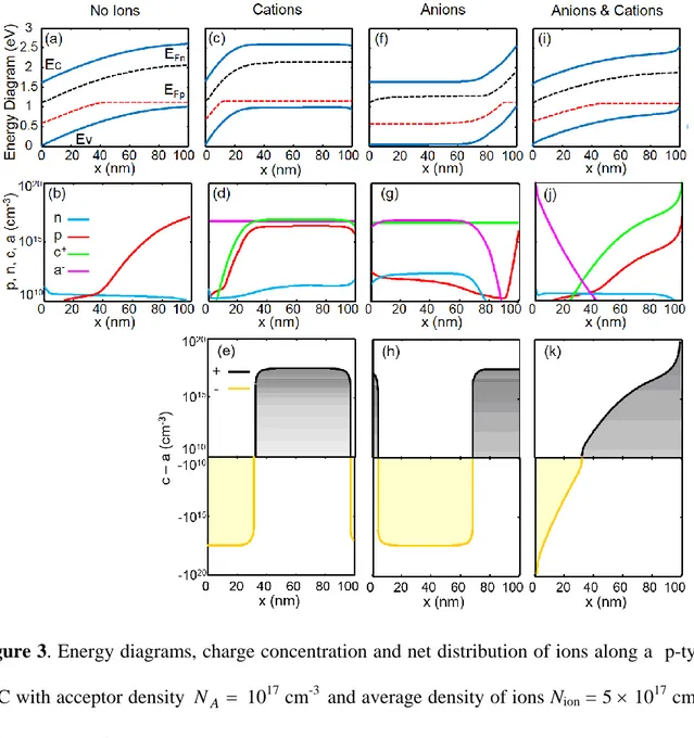
(18) resembling a dipolar structure similar to Debye layers mentioned previously. All the model equations and detailed description of calculations are presented in Supporting Information.. 3.1.. Effect of ionic species on the energy diagram of PSCs. In this section, the effect of the migration of one or two types of ions is analyzed. The starting ion distribution can be different from one to another dynamic experiment, and thus alter the interpretation of the experimental results. In order to study different possible scenarios, the following distributions for the cation c(x) and anion a(x) densities are considered. (i) a( x) c( x) N ion : ions are fixed and uniformly distributed. They are not allowed to move. The net ion charge density is zero. This is equivalent to consider no ions at all. (ii) a( x) N ion : the anion concentration is fixed and uniform. Only cations are allowed to move. (iii) c( x) N ion : the cation concentration is fixed and uniform. Only anions are allowed to move. (iv) Both types of ions are allowed to move.. 18.
(19) Figure 3. Energy diagrams, charge concentration and net distribution of ions along a p-type PSC with acceptor density N A 1017 cm-3 and average density of ions Nion = 5 1017 cm3, at short-circuit (Vapp = 0 V): (a)-(b) case (i) no ions; (c)-(e) case (ii) only cations move and the anion concentration is uniform; (f)-(h) case (iii) only anions move and the cation concentration is uniform; (i)-(k) case (iv) both ions move. The physical parameters used in the simulations are in Supporting Information.. The distributions of carriers, band bending, and internal electric field in steady state illuminated devices, calculated by DD method indicated in Supporting Information, for p-type PSCs at short-circuit condition are shown in Figure 3. The parameters used in the simulation are in Table S1. If only one type of ion is allowed to move, the resulting net distribution of 19.
(20) ions shows two uniform regions with opposite ionic charge (a positive layer at the anode and a negative one at the cathode) (Figure 3e,h). The net distributions of ions in Figure 3e,h are very similar. A very thin layer of negative charge inside the positive region close to the anode in Figure 3e, and a very thin layer of positive charge inside the negative region close to the cathode in Figure 3h are also observed. The origin of these thin layers comes from the small difference between the average ion-concentration Nion and the acceptor concentration used in the simulation. These tiny regions can be eliminated if the ratio between Nion and the acceptor concentration is increased. This is seen in Figure 4a-b where Nion =1018 cm3.. Figure 4. (a), (b) Net ion charge density c a along a p-type PSC at short-circuit with acceptor density N A 1017 cm-3 and average density of ions Nion =1018 cm-3, ( Vapp 0 V ) when only one type of ions moves (cases (ii) and (iii)).. If both type of ions move (Figure 3j-k), again, the positive ionic charge is displaced towards the perovskite-HSL contact and the negative one towards the ESL. However, the resulting net distribution of ions show thin layers where ions accumulate close to the interfaces. The accumulation of ions at the interfaces is combined with an accumulation of free charge of the same sign (holes at the HSL contact). This is an important result in order to explain the experimental observation of accumulation capacitance not only at open circuit but also at short circuit (commented later on, Ref. 144). In particular, we have observed that anions and holes accumulate close to the HSL-perovskite contact at short-circuit (Figure 3i) 20.
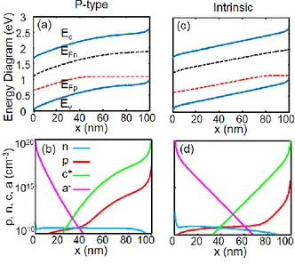
(21) and the same species close to the ESL in open-circuit (Figure S2 in Supporting Information). In both cases electronic charge is accompanied by accumulation of ionic charge of the same sign, which contributes to the slow time response observed. These different distributions of ions have a clear influence on the distribution of other electrical variables, which are analyzed below. The effect of these three distributions of ions on the energy diagrams is similar to increasing the dopant concentration in the device. They reduce the initial width of the depletion region seen in Figure 3a. The energy diagram of Figure 3c is similar to a highly p-doped semiconductor. The energy diagram of Figure 3f is similar to a highly n-doped semiconductor, although no additional electrons are created. Figure 3i shows a similar band diagram to that of Figure 3a. However, a stronger accumulation of holes at the perovskite-HSL contact can be observed in Figure 3i-j in comparison with Figure 3a-b. Results at open-circuit condition for the same situations are shown in Supporting Information.. 3.2.. Effect of the type of semiconductor conductivity. In this section, the analysis made for p-type PSCs at short- and open-circuit steady states is repeated for intrinsic PSCs. In this comparison, we consider that both anions and cations are allowed to move. For consistency, the same simulation parameters are used, including the same values for the metal-perovskite contact barriers (a rectifier contact at the cathode and an ohmic contact at the anode). This study is important to clarify open questions about the nature of the perovskite semiconductor.[3,. 8, 61]. In particular, we discuss whether the electric field. penetrates uniformly into the bulk semiconductor or not. According to our calculations, similar results are extracted in both p-type and intrinsic cases (Figure 5). No compensation of the internal electric field is seen in any region in the two cases, despite some suggestions of an electric field compensation at short-circuit operation due to the accumulation of ions at the interfaces.[3, 5, 6, 9] Intrinsic and p-type PSCs are also compared at open-circuit after, observing no differences between these two cases (Figure S3 in Supporting Information). In the rest of 21.
(22) this work, we consider a p-type perovskite and the presence of both anions and cations in agreement with recent works in which the electronic transport is attributed to holes and the ionic transport to the iodide ions and their respective vacancies.[35, 36, 54]. Figure 5. Comparison of energy diagrams (a), (c) and charge densities (b), (d) in p-type and intrinsic solar cells at short-circuit ( Vapp 0 V ). Both anions and cations are allowed to move in the device.. 3.3.. Dipolar distribution of ions. In the previous section, we have seen that different distributions of ions in a PSC produce different distributions of electric field inside the semiconductor, leading to different performances of the device. In this section, the DD distribution of ions (or exact steady state distribution) is compared to a dipolar ion distribution. This dipolar distribution can be considered as an approximation of the first one (Figure 3), as shown in the bottom panels of Figure 6. This is a usual approximation found in the literature in order to obtain quick simulation approaches.[4,. 9, 19]. The electric field, band bending and charge densities in. illuminated devices are determined for different dipolar distributions. Finally, a comparison with the results obtained with the DD distribution is made.. 22.
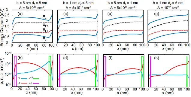
(23) Figure 6. (a), (c), (e), (g) Energy diagrams and (b), (d), (f), (h) charge concentration of electrons, holes, anions and cations at short-circuit with the physical parameter values depicted above the figures.. The sign of the charges in the thin layers is assigned in agreement with the sign of the charge found close to anode and cathode in the DD distributions at short-circuit and opencircuit, as described in detail in Supporting Information. As mentioned before we have anions accumulate close to the anode at short-circuit and close to the cathode in open-circuit. Cations accumulate close to the opposite contact. Here, we study three cases by changing one of the three parameters and keeping the other two of them constant: (i) the thickness of the sheets b , (ii) the distance of the layers to their closest interface d l , and (iii) the value of the ion density per unit area A. Figure 6 shows the results of the numerical simulation of a PSC at short-circuit for different values of b , d l and A . Two regions within a distance b d l to the contacts act as a planar capacitor of thickness b d l . In each contact region, a voltage Vcontact drops. In the central region, a voltage Vbulk drops. The effect of varying the thickness b , case (i), can be analyzed after the comparison of Figure 6a-b and Figure 6c-d. We observe that the higher the value of b is, the higher the value of Vcontact drops along the contact region and the lower the 23.
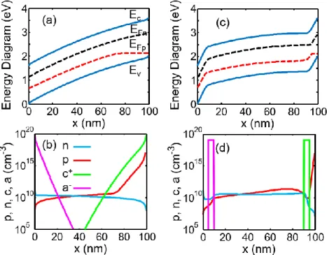
(24) value of Vbulk drops along the bulk (Figure 6a). The similar electric field close to the contacts in Figure 6a and Figure 6c is accompanied with no changes in the charge carrier concentrations within a distance d l next to the contact regions. In Figure 6c, the energy bands are flatter in the bulk, and the carrier concentrations are lower and more uniformly distributed along this central region. Thus, a change in the distance b d l (with A constant) reduces the intensity of the electric field in the bulk, minimizing the effect of the drift mechanism (Figure 6c). The effect of varying d l (case (ii)) is seen after the comparison of Figure 6a-b and Figure 6e-f. The bands in the bulk bend in opposite directions in Figure 6a and Figure 6e. The drifting effect is not only softened but inverted. The cases (i) and (ii) lead to similar conclusions: the displacement of the ionic layers closer to the boundaries is equivalent to making these layers narrower. Case (iii) analyzes the effect of changing the value of A . The energy diagrams and free carrier concentrations of Figure 6g are practically identical to the ones of a perovskite without ions (Figure 3a). A similar study with the parameters b , d l and A of the dipolar distribution for open-circuit is detailed in Figure S5 (SI).. 3.4.. Comparison of the DD and the dipolar distribution of ions. One of the main differences obtained for the dipolar distribution is the compensation of the internal electric field in the bulk seen at short-circuit. This is observed in Figure 6a,c,e but not in the DD distribution of Figure 3i. The ion density per unit area A in the dipolar distribution must be decreased (Figure 6g-h) in order to achieve similar band diagrams as in Figure 3i. The differences between the DD and dipolar distributions seen at short-circuit can also be observed at reverse voltages. An example is in Figure 7 where the DD and dipolar distribution cases are compared at deep reverse bias Vapp 1 V . At this voltage, the ions. 24.
(25) tend to accumulate closer to the contacts than at Vapp 0 V (Figure 3j).. Figure 7. Energy band diagram and distributions of ions, electrons, and holes for a p-doped PSC under illumination at Vapp 1 V , (a, b) including drift-diffusion of ions in the numerical simulation and (c, d) assuming a fixed dipolar-distribution of ions in the numerical simulation.. The other interesting feature for the dipolar distribution is the existence of an electric field located in the bulk of the absorber layer that opposes the internal electric field at short-circuit Figure 6a,c,e and not existing in Figure 6g. The electric field seen in the bulk of Figure 6a,c,e facilitates the collection of charge at the electrodes, thus increasing the photocurrent close to the short-circuit region. As mentioned before, some authors suggest that ionic charge accumulates at the edges of the perovskite in the Debye layers.[4, 19] From this comparative analysis (Figure 3 and Figure 6 for short-circuit, Figure 7 at Vapp 1 V , and SI for opencircuit) the surface band bending associated with Debye layers is detected only in the dipolar 25.
(26) distribution of ions (Figure 6 and Figure 7c). For the DD distributions of ions, the bands bend very slightly close to the perovskite interfaces (Figure 3i and Figure 7a), not showing this Debye layer. It is immediately apparent that the distribution of the ions and carriers for the DD and dipolar distributions will have a strong impact on the device performance. The large neutral region in the bulk of Figure 6a,c,e shows that the photogenerated carriers in the bulk will be separated mainly by diffusion to the contacts, as opposed to Figure 3i where the ions create their own electrical field through the device, which facilitates charge separation similar to the case without ions. The charge extraction at the contacts in both cases (DD and dipolar distributions) should also be different. In the case of the dipolar distribution, steep potential drops at the contacts can serve as preferential recombination sites for photogenerated carriers (surface recombination), and indeed this is often used to explain the large reduction in opencircuit potential when scanning from short-circuit to open-circuit.[3] It must also be noted that these Debye layers provide large injection-extraction barriers for the carriers, and consequently, the device performance is mostly controlled by the efficacy of charge extraction and recombination at the contacts itself rather than any transport considerations. Overall, the approximation of the exact steady state ion distributions by means of dipolar distributions is a reasonable starting model, but it must be used carefully because changes in the parameters that determine the dipolar distribution of ions affect the net distribution of electric field in the perovskite semiconductor significantly. Another important conclusion is about the discussion of the general doping character of the hybrid perovskite and the basic energy diagram model, i.e. whether the barrier is close to one interface, or the built-in voltage produces a slanted band as in a p-i-n solar cell. Our calculations show that so far as the moving ion density is significant and close to the native doping density, the moving ions determine the barrier and field distribution irrespective of the conductivity nature of the perovskite, such as p-type or intrinsic semiconductor. Therefore, 26.
(27) one needs be aware that pretreatments of the device may produce important and sometimes irreversible changes in the operation of the solar cell, as shown experimentally.[67]. 4. Transient response measurements The physical phenomena occurring in a perovskite solar cell span an impressive range of diverse timescales, from the phonon response for charge shielding and cooling of photogenerated carriers in picoseconds time to the slow relaxation at room temperature that may take seconds. In the next sections of this review, we will describe a variety of techniques which are used to probe the different phenomena that occur in the slow side of the general time scale, i.e. from microseconds to seconds. Time transient experiments as well as frequency domain techniques are surveyed. Here, we aim to bridge the gap between fundamental properties and device operation. Therefore, we need to measure full devices with contacts and determine the observations corresponding to different relevant phenomena such as transport, recombination, charge injection and ion drift, identifying if possible the locus of the physical signal, i.e. the bulk of the absorber, grain boundaries, or outer interfaces. We present a selection of important descriptions and explanatory experiments approaching central aspects of the unique phenomenology of PSCs. With this purpose, we first comment on methods of transient time measurements at different time scales, as well as the consideration on recombination. Subsequently, in Section 5, our attention will be focused on the charge accumulation by discussing the capacitance ( C ) with the associated resistance ( R ). In our program to cover the main aspects of the device operation for practical purposes, the hysteresis of J V curves plays a dominant role and this issue will be approached in Section 6.. 4.1.. Characteristic response times and basic transient behavior. For characterizing the response time domains and transient behavior of PSCs, several 27.
(28) techniques and particular experiments have been reported in the literature. In general, given the significant variety among device designs (e.g. materials, structure of layers) and fabrication procedures (e.g. composition, variables during processing), certain scattering is often found for most measurements on these devices. However, general features can be highlighted as typical and even unique, especially when samples of large quality and efficiency become available Obviously, in the focus of our approach, the electron-hole recombination mechanisms play a fundamental role. These are (i) the radiative recombination and the non-radiative (ii) Shockley-Read-Hall (SRH) and (iii) Auger recombinations. While in the first case a photon is emitted, in the SRH recombination, the electron relaxation is assisted by midgap states (traps) and the energy is dissipated as lattice vibrations. In the other case, the Auger recombination occurs when the energy is given to a third carrier, which accesses a different kinetic energy in the same band and then is often thermally relaxed. It should be noticed that the absorption coefficient of MAPbI3 is quite remarkable for having an unusually sharp shoulder near E g with higher values than most other comparable semiconductors, which can be observed in Figure 8a. This abrupt optical band edge exhibits a clear exponential law exp[h / EU ] with the photon energy h . The resulting Urbach tail energy EU 15 meV is far lesser than a-Si and CIGS solar cells. Actually, it approaches those of other successful direct-band-gap materials such as GaAs and CdTe.[68,. 69]. Therefore,. contrasting indirect-band-gap materials like a-Si, the low EU of MAPbI3 suggests a very low degree of structural disorder and the purely exponential Urbach tail means that no optically detectable deep states are present in the MAPbI3 material. This is a key element for explaining the large achieved Voc values around 1.1 V, whose non-radiative losses has been estimated around 230 mV from the radiative Voc limit of 1.33 V.[70]. 28.
(29) Figure 8. (a) Absorption coefficient spectra of high quality semiconductors in photovoltaic technologies, as indicated. Adapted with permission.[68] Copyright 2014, American Chemical Society. (b) PL spectrum and corresponding absorbance (in Tauc plot representation for direct band-gap recombination) of a TiO2/MAPbI2 layer showing virtual absence of Stokes shift around the band-gap: 1.6 eV (775 nm). Data courtesy of Thi Tuyen Ngo (INAM). (c) PL decays from different pulsed fluences in a MAPbI3-based device. Adapted with permission.[71] Copyright 2017, American Chemical Society. (d) Evolution of normalized PL intensity under continuous excitation for three different devices of distinct perovskite and fabrication procedure. Reprinted with permission.[17] Copyright 2014, American Chemical Society. (e) Evolution of the normalized EL signal of a working device under air and nitrogen atmosphere at constant voltage (1.5 V). The inset shows the evolution of the signal at a shorter time-scale window. Reprinted with permission.[72] Copyright 2015, American Chemical Society.. The radiative recombination in MAPbI3 is basically due to band-edge electrons and holes, as is evident from the nearly absent difference (at most 10 meV) between the absorption onset and the photoluminescence (PL) peak, i.e. the Stokes shift.[30,. 70, 73, 74]. This is illustrated in. Figure 8b where PL and absorbance (in Tauc plot representation) spectra are compared. In contrast, some singularities in alternative perovskites can be mentioned. For instance, in the 29.
(30) work by Wright et al.,[75] the Stokes shift in FAPbI3 was found to be temperature dependent and larger when the excitation fluence was reduced. Moreover, for CsPbBr3 nanocrystals, it is enhanced to hundreds of meV. as the nanocrystals edge length are reduced to a few. nanometers[76] and even anti-Stokes shift has been found in MAPbI3-xBr.[77] As a basic practice for testing radiative recombination, the samples are typically pulsed with a nearly monochromatic light source and the PL decay is recorded in order to estimate the PL lifetime. For PSCs, these measurements report values from tens to, unusually, hundreds of nanoseconds, extracted from the fitting to a mono-exponential law that characterizes the dominant radiative recombination path. Nevertheless, in some studies, a twotime constant PL decay has been found[78-81] with the consequent consideration of competing recombination mechanisms. In this context, the work by Kanemitsu and co-workers[30] particularly showed that PL decay curves are sensitive to the excitation fluence, as in Figure 8c, and that the PL decay dynamics are well explained by the free-carrier band-to-band recombination rather than the exciton recombination. The latter was concluded from the absence of Stokes shift (lack of non-radiative recombination increase) at larger excitation fluences, when the PL decays are faster and two time constants appear. In addition, they also proposed that photon recycling could be the responsible for the unusual slow PL decay.[30] On the other hand, other singular behaviors were reported by Sánchez et al.,[17] who measured the evolution of the PL intensity under continuous excitation for different device structures and fabrication procedures. Two decaying intensities (Sing-MA/I-Cl and Seq-MA/I in Figure 8d) and an increasing one (Seq-FA/I in Figure 8a) were noticed. The PL intensity drop, was attributed to the increase of the nonradiative losses, the increase of charge separation rate toward regions such as grain boundaries, abrupt changes in the absorption spectrum of the perovskite upon illumination as a consequence of the dielectric polarization or anisotropic absorption of the different light polarization angles. This latter explanation, upon reaching the dielectric polarization of the device, would be compatible with the slight PL enhancement for the Seq-FA/I sample. Complementary to the reversible PL responses of 30.
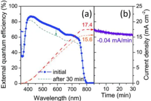
(31) Figure 8a, a subsequent study[72] also showed the electroluminescence (EL) evolution with time at a constant applied bias. It was shown that the EL presents a mostly-irreversible increase followed by a quenching in different time scales depending on the atmosphere composition. Returning to the PL decays from different pulsed excitation intensities, Handa et al.[71] made an interesting combination of these results (fluence dependence of time constants) with photocurrent (PC) measurements, proving a significant reduction of the external quantum efficiency (EQE) above a certain level of illumination. The direct implication here is that the carrier-injection rate is sensitive to the photogenerated carrier density, meaning that a carrierinjection bottleneck strongly enhances recombination losses of photocarriers in the perovskite layer at high excitation conditions. Moreover, they discarded the influence of Auger recombination for photocarrier densities below 1017 cm-3 . Additional irregularities were noticed by Unger et al.[15] from their study of full EQE spectrum evolution with time and corresponding J sc change. As displayed in Figure 9a, after half an hour, the spectral shape of the EQE did not change substantially between repeated scans, but a vertical shift appeared in correspondence to the current reduction by that time in Figure 9b. This suggests that the PC decay results from a reduction in the charge extraction efficiency rather than optical changes to the absorber or contact layer. Consequently, a direct macroscopic implication arises here from these slow transients: a serious unreliability can be found with the matching between integrated EQE values and PC densities determined from. J V measurements, mainly at long delay times or steady state PC measurements. Furthermore, the evaluation of complementary important parameters can be similarly affected for these anomalous behaviors. That is the case, for instance, of the yielded open-circuit voltage radiative limit obtained from EL and EQE, as presented by Tvingstedt et al.[70] and Tress et al..[82]. 31.
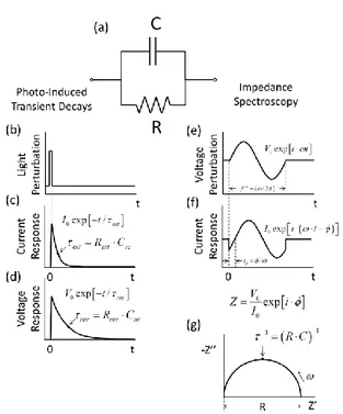
(32) Figure 9. Reversible evolution of EQE spectrum (a) and corresponding J sc (b). Adapted with permission.[15] Copyright 2014, Royal Society of Chemistry.. At this point, it is already clear that the competition of several factors affecting the charge extraction, also evidenced in the radiative recombination, produce a noteworthy time change in recombination, and thus current. Here is precisely where several studies have been focused on, e.g. dealing with the evolution of PC and open-circuit voltage ( Voc ) under different configurations, perturbation types and devices characteristics. As in Figure 10b-d, one basic approach is to apply a light perturbation and record the subsequent response. For instance, in the simplest case, when the sample behaves nearly as an RC circuit (Figure 10a), the current at SC should decay exponentially with an extraction time constant ext Rext Csc and the voltage at OC with a recombination time rec Rrec Coc . However, as we will comment in the following section, for PSCs it can be quite challenging to actually obtain such “textbook” experimental relaxations.. 32.
(33) Figure 10. Two different ways to evaluate the characteristic time constant of a sample that ideally behaves like a RC circuit (a): by photo-induced transient decays (b-d) or by impedance spectroscopy (e-g). In each case, the perturbation (above) and the response (below) with time are displayed. Additionally for the IS the corresponding Complex plane plot is shown (f).. Among the most common practices one can find in the reports from several groups are those of photo-induced (PI) transient photocurrents (TPC) and transient photovoltage (TPV), where typically the signal produced by a small light pulse perturbation is recorded in SC and OC conditions, respectively.[83, 84] The main aim of acquiring TPV is to evaluate the lifetime of the charge carriers as a measure of the recombination in the sample, while the TPC provides a quantification of the amount of charge produced by the device given a certain illumination, being evidently the time rec (at OC) larger than ext (at SC). In addition, a tricky sequenced combination of illuminated OC and dark SC is also often used to measure the charge evolution at a given Voc in the photo-induced charge extraction (PI-CE)[83-85] technique. A two time constant decay process was first identified in this context by Sánchez et al.[17] by measuring PI-TPV on several configurations. Subsequently O‟Regan et al.[86] conducted a 33.
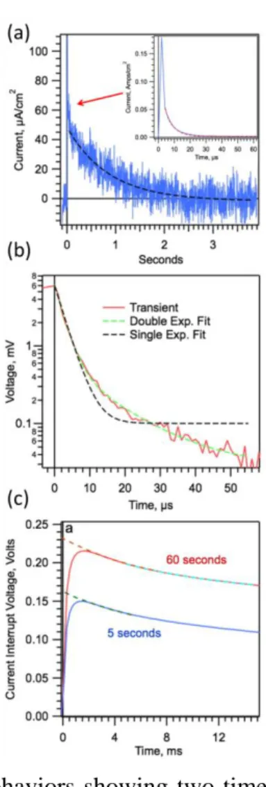
(34) broader description during their studies on PI-TPV, PI-TPC and PI-CE. Illustratively, PI-CE measurements at 1 sun showed a transient photocurrent decay of 180 mA cm-2 in about 50 μs (inset of Figure 11a) while the remaining 50 μA·cm-2 needed seconds to relax (Figure 11a bottom axis). Importantly, the integrated charge collected for the slow decay (~3.6×10⁻⁵ C·cm2. ) was about 50 times higher. Similarly, the PI-TPV decays at 1 sun were found to present a. fast component of 1-2 μs and a slow part around 5-10 μs, as observed in Figure 11b. Subsequently, further reasoning[87] associated the fastest lifetime from the PI-TPV with recombination processes. They also suggested that reorganization of dipoles could explain the slowest relaxations. Interestingly, current interrupt voltage measurements were also shown to evolve in the domain of milliseconds, as shown in Figure 11c. By switching from illuminated SC to dark OC, the sample voltage rises during ~ 2 ms up to a peak while charge is transported toward the contact electrodes and hence it decays during tens of milliseconds due to recombination.[86] Importantly, the time of SC illumination enhances the Voc peak, possibly indicating that it increases the band offset at the voltage generating interface(s) in the cell. Subsequently, Palomares and co-workers[88] compared the two time constant TPV decays between devices with and without mesoporous TiO2 and also looked at the transient absorption spectroscopy (TAS)[84] patterns. The results showed apparent differences only for the slowest recombination time and therefore, they assigned the fastest component to recombination between electrons in the MAPbI3 and holes in the HSL.. 34.
(35) Figure 11. Different transient behaviors showing two time regimes. (a) Current decay from PI-CE set up with the first 60 s of SC (fast transient) in the inset. (b) Experimental PI-TPV and theoretical fitting with mono- or double-exponential relaxation laws. (c) Dark Voc decay following current interrupt from illuminated SC with similar J sc but during different times, as indicated. Adapted with permission.[86] Copyright 2015, American Chemical Society.. 4.2.. Slower than seconds relaxation processes. Beyond double exponential decays, the work of Baumann et al.[89] identified three distinct time regimes during the Voc decay at OC under several pulsed illumination intensities ranging from 1-100 mW·cm-2. Importantly, while the two first characteristic time constants were of 10-100 μs and 1-100 ms, respectively, the third phase of the decay was as slow as 10 s. As 35.
(36) illustrated in Figure 12, this behavior is different from that of organic solar cells (OSCs) whose decays can be fitted to a single exponential along almost the complete transient. In all the cases, the slowest process was associated with shunting and the apparent illumination dependent recombination once more became a target of further discussion keeping in the core of debate the influence of the interface. About the latter, Nagaoka et al.[90] also found similar decays but specifically pointed to the sensitivity to the nature of the perovskite/ESL interface. Moreover, Bertoluzzi et al.[91] attempted to separately inspect the fast and slow components by measuring short lifetimes with typical PI-TPV (pulsed constant small perturbation with different background illuminations) and the large time constant from Voc decays (switch from light to dark at OC) at different illumination intensities, also known as open-circuit voltage decay (OCVD). Their results corroborated 100 μs and 1 ms for the faster components whose meaning was ascribed to discharge and recombination of photogenerated electrons and holes. However, the third and slowest component, with an estimated characteristic time up to 100 s, was found to behave as a power law decay relaxation. Ionic-electronic polarization and depolarization kinetics depending on internal voltage were proposed as explanation. Importantly, they introduced the useful concept of instantaneous relaxation time defined as 1 dV . 1. (2). ir . V dt . This parameter straightforwardly gives a criterion on the presence or not of exponential relaxation decays and it also illustrates the characteristic time constants or domain.. Figure 12. Photovoltage decay of a MAPbI3 based solar cell (green) and two OSCs (red and 36.
(37) blue) for different illumination intensities, as indicated. Differently to OSCs, the PSC decay is divided in three time regimens. Reprinted with permission.[89] Copyright 2014, AIP Publishing in accordance with the CC BY 3.0 license.. Furthermore, the effect of prior light soaking was found to be determinant on the shape of the OCVD, as described in the contribution of Gottesman et al..[8] The two types of OCVD response are shown in Figure 13a and the related ir are presented in Figure 13b, where the differences are evident after the initial fast decay (~1.0-0.8 V) that is out of the resolution of this experiment. Initially, or when dark recovery is set before the pulse, a slow decay of seconds take place when Voc goes from 0.8 V to 0.2 V with the competition between exponential (plateaus in Figure 13b) and power law (monotone regions in Figure 13b) relaxation decays. Subsequently, an even slower power law relaxation occurs during more than 10 s. Differently, when light soaking is set before the pulse, a faster exponential decay reduces Voc from 0.8 V to 0.2 V with a time constant of 10 ms and the slowest power law relaxation takes at least an hour to remove the remaining electrostatic internal potential Velec . In other words, light soaking (i) makes the initial Voc decay faster but (ii) slows down the final part of the decay where an extra Velec takes considerably more time to relax. Regarding the first issue, the light soaking conditioning of fast recombination was stated in terms of major changes in the contact region deduced from physical simulations. Likewise, other modeling results illustrated that Velec is possibly sustained by the charge accumulation of slow, mobile positive ion charges and electronic holes in a double layer at the perovskite/ESL interface, as shown before in Fig. S2. These results were subsequently corroborated by Hu et al.[92] on diverse device configurations. Additionally, they measured the Voc as a function of the illumination intensity with and without light soaking preconditioning. They observed a clear. Voc reduction after light soaking above a given illumination level, which they attributed to 37.
(38) large surface recombination of accumulated electronic carriers at the perovskite/ESL interface upon light soaking.. Figure 13. Effect of light soaking in the Voc of PSCs. (a) Dark transient Voc after long term storage in dark (Reference), light soaking (6 minutes), and again dark recovery (1 hour). Reprinted with permission.[8] Copyright 2016, Elsevier. (b) Instantaneous relaxation time from OCVDs similar to those of (a) for PSCs with different ESL and with prior light or dark soaking times, as indicated. During light soaking, at least three time regimens are identified and from dark recovery, the relaxation can be possibly divided in 4 stages, as indicated. Adapted with permission.[91] Copyright 2015, Royal Society of Chemistry.. However, besides light soaking, the polarization history or pre-poling has been found to directly modify the internal processes behind the slow mechanisms too. Figure 14 shows the J sc after switching from OC to SC under constant 1 sun illumination for two preceding. reverse applied voltages measured by Chen et al.[93]. Once more, the separation between faster and slower responses takes place. Independently of poling, a quicker decay occurs in all cases in a time scale from milliseconds to seconds presumably associated with capacitive effects due 38.
(39) to electrode polarization. Afterward, for the transient without poling, the J sc reaches its constant equilibrium level, which is the general shape of the response, although in some reports[6,. 90]. , the possibly capacitive transient can last tens of seconds. In contrast, as the. reverse poling increases, a larger reduction of J sc happens that relaxes toward the equilibrium level during about 100 s. This second process could be explained in terms of contact barrier modification due to interface ionic charges. Illustrative of the ionic nature of charge balance at the interfaces, measurements by Almora et al.[64]. on MAPbI3 showed a typical Guoy-. Chapman diffuse layer performance.. Figure 14. Dynamic J sc transient behavior when switching from OC to SC for unpoled and reverse poled conditions. Reprinted with permission.[93] Copyright 2015, American Chemical Society.. 5. Impedance and capacitance features of perovskite solar cell devices So far, the evaluation of time domains during the electrical responses has been reviewed aiming to illustrate how the current and voltage evolve under different conditions. An alternative and very useful method uses a small perturbation signal in the frequency domain. As there are different alternative approaches, we provide a short introduction of impedance spectroscopy, centered on capacitance, and evaluation of similar quantities by the small perturbation time transits.. 39.
(40) 5.1.. Definitions. For convenience, here we first introduce a set of important clarifying concepts as well as experimental set-up descriptions which will be systematically alluded to in the subsequent sections. Interpretation of measurements and measured quantities. The impedance spectroscopy (IS)[94] analysis has been widely used for the characterization of solar cells.[95] In general, the impedance is the measurement of small perturbation voltage ( Vˆ ) to current ( Iˆ ). In the potentiostatic variant, the IS basically consists of applying an AC potential small perturbation Vˆ V0 exp it at a given frequency f / 2 (using the complex numbers representation where i is the imaginary unit) with respect to the angular frequency as in Figure 10e. Subsequently, the AC current response Iˆ I 0 exp i t of the sample (Figure 10f) is detected, being the phase shift between perturbation and response. The impedance is defined as Z ( ) . Vˆ ( ) Iˆ( ). (3). The real and imaginary parts of the impedance, Z ' and Z '' respectively, are obtained as (4). Z ( ) Z iZ . For an ohmic process, the impedance is a constant, Z R , the resistance, that is a positive and real quantity. Under modulation of any system, the kinetic processes produce a frequency dependent response that includes imaginary values. For the simplest case of an RC circuit, shown in Figure 10(a), the complex plane plot representation, Z ''( Z ') in Figure 10g, exhibits a semicircle. The characteristic time is. 1 RC. (5). with respect to the angular frequency that marks the top of the arc. Note that the characteristic resistance R is obtained at zero frequency, Z (0) R . The value 0 in. 40.
(41) parenthesis indicates that the displacement is infinitely slow, i.e., Vˆ (0) and Jˆ (0) attain a value that is independent of time. For a solar cell with area A , the quotient of the small quantities gives. Z (0) . 1 Vˆ (0) dJ A Rdc A Jˆ (0) dV . (6). That is, the small quantities give a derivative of voltage with respect to current. This is the reciprocal of the slope of the J V curve, which is in turn the dc resistance of the solar cell. Rdc (per area) in those particular conditions. In real systems, there is at least a series resistance element that shifts the arc towards the right in Figure 10g, and multiple pairs of capacitive and resistive elements can add and/or deform arcs in the complex plane plot. In addition, inductive and/or non-linear elements can also complicate the IS spectra. Concerning the PSCs, a more detailed discussion on the general characteristics of the impedance spectra will be provided in Section 5.5. However, at this point, it is instructive to highlight that no less than two arcs are often presented in the complex plane plots for these devices, at low and high frequency respectively. Therefore, each arc may correspond to an individual mechanism with its own time constant. In this context, several IS studies have reported lifetimes in good agreement with the transient photo-induced measurements,[17] at least with one of the RC constants. In a discharge experiment in the time domain decay method, we apply a small step of the voltage Vˆ (t ) V u (t ) , u(t ) being. the unit step function at t 0 , and we observe the. consequent evolution of the charge Qˆ (t ) that passes to the system. However, it is not usually feasible to measure a charge transient, thus we need to observe the current transient Iˆ(t ) and perform an integration: t Qˆ (t ) Iˆ(t )dt . (7). 0. Let us look at this process in the frequency domain. We use the variable s i , with. 41.
(42) i 1 . The Laplace-transformation of a function f (t ) to the frequency domain is defined as . F (s) e st f (t )dt. (8). 0. Application of the transform to Equation (7) gives Iˆ(s) Qˆ (s) (9) s . Now we introduce a frequency-dependent capacitance that indicates the modulation of. charge with respect to voltage. C * ( ) . Qˆ ( ) Vˆ ( ). (10) . C * ( ) is a function of the frequency, that coincides with the static differential capacitance. C at 0 , as follows. C. Qˆ (0) Vˆ (0). (11). where. dQ . (12) dV We now remark that representing either impedance or capacitance is a matter of choice. C. Both functions correspond to the same measurement, since they are connected by Equation (9), indeed:. C * ( ) . Iˆ( ) 1 i Vˆ ( ) i Z ( ). (13). or more explicitly. C * . Z '' i Z ' . . Z ' Z '' 2. 2. .. (14). However, with respect to graphical presentation, both magnitudes show different information. For a resistive/conductive/recombination process, the arcs in the complex 42.
(43) impedance plane show immediately the different components of resistance, while the capacitance is hidden. On the other hand, a plot of the real part of the capacitance vs. frequency reveals very clearly the charge storage modes of the system that we describe in detail below. Here, we also note that the usual normalization convention considers capacitance in units of Farads per unit area (e.g. F cm-2 ). Accordingly, analogous definitions to Equation (10) to (12) should be used, but with the charge expressed in Coulomb per unit area (e.g. C cm-2 ). Similarly, impedances and resistances like in Equation (13) to (14) may be presented in Ohms per unit area (e.g. cm2 ). Physical interpretation of the capacitance. The most basic capacitive response from a solar cell is that of the geometrical capacitance C g , which only accounts for the sum of the dielectric contribution of each layer between the metallic electrodes. For the typical case of thin film heterostructures, where the classic parallel-plate capacitor is a suitable model, the geometric capacitance per unit area of a device of m different layers in series can be obtained as 1. C g m 0 ,m dm , 1. (15). where d m is the thickness of the m-th layer and ,m its relative dielectric constant towards the limit . Obviously, from Equation (15) it is clear that C g can be dominated by the layer whose dielectric capacitance is lower in comparison with the rest. Actually, C g is in general the smaller characteristic capacitance of a sample, thus frequencies above 1 MHz are often needed to determine it.[96] A second capacitive response to mention is that of the accumulated charge at the edge of the depletion layer in p-n junction-based devices. In the one-side abrupt charge density profile approximation[97], (same as used in Section 3), the depletion layer capacitance per unit area 43.
Figure
+7
Documento similar
• Telemetry processor will use a look-up table, initially populated by values obtained in simulation, to update the control loop gains based on its r 0 and noise variance
The environmental impacts affecting human health during the life cycle of the solvents used in perovskite film 194.. manufacturing, including production, removal and EOL for the
In this work, we show that pure FAPI perovskite solar cells (PSCs) have a dramatic increase of device long-term stability when prepared under ambient air compared to FAPI PSCs
The newly formed FAPI-PbS QDs are dissolved in FAPI solution for the fabrication of perovskite thin films for the characterization and device applications
Despite the excessive energy consumption and the great uncertainty of the laboratory- based single-junction and tandem PSCs, their environmental impacts are lower than for silicon PV.
Power law voltage decay in perovskite solar cells shows cooperative relaxation phenomena..
prepared a triad consisting of a Fc unit linked to a zinc triarylporphyrin through a benzo-amido-benzo spacer, and a 4-pyridylnaftalnediimide axially coordinated to the zinc
Two related families of star-shaped thiophene-containing small molecules based on fused tetrathienoanthracene (TTAn) and non-fused tetrathienylbenzene (TTBn) cores are tested
