solar cells
I. Garcia , I. Rey-Stolle , C. Algora , W. Stolz , K. Volz
a
Institute) de Energia Solar, E.T.S.I. Telecomunicacion, Universidad Politecnica de Madrid, Spain
b
Material Sciences Center-Central Technology Laboratory and Department of Physics, Philipps University Marburg, 35032 Marburg, Germany
A B S T R A C T
The ordering phenomenon produces a reduction in the band gap of the GalnP material. Though a
drawback for many optoelectronic applications, ordering can be used as an additional degree of material
and device engineering freedom. The performance of the record efficiency GalnP/GaAs/Ge multijunction
solar cells depends on the quality and design of the GalnP top cell, which can be affected also by
ordering. The tradeoff existing between band gap and minority carrier properties, and the possibility of
creating a back surface field (BSF) structure based on an order-disorder GalnP heterostructure makes
the study of the ordering appealing for solar cell applications. In this work, the ordering dependency
Keywords: with the growth conditions and substrate orientation is studied. The results obtained are presented to
Al. Ordering enrich and extend the data available in the literature. Then the properties of order-disorder GalnP
A3. Metalorganic vapour phase epitaxy heterostructures are assessed by using them as BSF in GalnP concentrator solar cells. The external
B1 CalnP
. .. quantum efficiency (EQE) shows a good behavior of these BSF layers, but unexpectedly poor electronic
quality in the active layers. Although the exact origin of this problem remains to be known, it is
attributed to traps introduced by the ordered/disordered domains matrix or growth native defects. EQE
measurements with bias light show a recovery of the minority carrier properties, presumably due to the
saturation of the traps.
1. Introduction
GalnP grown lattice matched to GaAs exhibits anomalous
changes in the band gap depending on the growth conditions and
the substrate misorientation. These changes are the result of the
spontaneous ordering during the growth of the cation-site
elements (Ga and In) in planes parallel to the (111) . This
gives rise to a Cu-Pt structure, which results in a lowering of the
band gap of the material, whose exact value depends on the
degree of ordering. Reductions above 100 meV can appear. This is
sometimes a drawback due to the red-shift of the emission of
optoelectronic devices made with ordered GalnP. However, the
relation between ordering and band gap provides a new degree of
freedom when working with GalnP. For example, sharp O/D GalnP
structures can be created by just changing the
tertiarybutylpho-sphine (TBP) partial pressure during growth
Three-junction GalnP/GaAs/Ge concentrator solar cells have
achieved record efficiencies exceeding 40% . The theoretical
calculations for this combination of materials indicate that, to
achieve maximum efficiencies, the band gap of the GalnP top cell
should be as high as possible, i.e., the GalnP should be completely
disordered . However, the MOVPE growth conditions that produce
such a material have deleterious effects on other important aspects
like surface morphology or minority carrier properties, which
determine the performance of the solar cell. In practice, the usual
band gap of the GalnP lattice matched to GaAs suitable for solar cell
applications is 1.85 eV. On the other hand, a current matched
multijunction device must be obtained to maximize its conversion
efficiency. Since at the same time, it is desirable to have a
short-circuit current as high as possible, the GalnP top cell must absorb the
minimum amount of light with maximum conversion efficiency. The
usual technique to achieve this consists on thinning the top cell base
layer. This makes this layer more sensitive to the quality of its
interface with the layer underneath. To improve the conversion
efficiency, an effective back surface field (BSF) layer must be
inserted. Again, GalnP ordering can play a role in this aspect, for it
is possible to grow a BSF structure based on an order-disorder GalnP
layer stack . To achieve this, the growth conditions must be
chosen carefully for the active (emitter and base) and BSF layers. The
description and results of such a task is the aim of next sections.
2. Experimental procedure
trimethylindium (TMIn), tertiarybutylphospine (TBP), tertiarybu-tylarsine (TBAs), trimethylaluminium (TMAl), diethylzinc (DEZn) and ditertiarybutylsilane (DTBSi2). Using TBP is especially
advantageous in this case, because it allows the achievement of sharp order–disorder GaInP heterostructures with a variation of the V/III ratio during growth, which is not possible if PH3is used [2]. The work pressure was 50 mBar and the temperature was corrected using the Al/Si eutectic method. All the experiments were preceded by a cleaning and coating run consisting on a baking of the susceptor at 8001C and a deposition of about 1
m
m of GaAs. This was done to prevent the In and P coming from the GaInP terminated runs to affect the following experiments. After the epitaxial process, all the samples were systematically characterized with the high-resolution X-ray diffraction (HRXRD), room-temperature photoluminescence (RT-PL) and AFM techni-ques. For the solar cell external quantum efficiency (EQE) measurements, a monochromator-based system is employed with a chopped light beam. The detection is made by means of the lock-in technique.3. Ordering vs. growth conditions and substrate misorientation
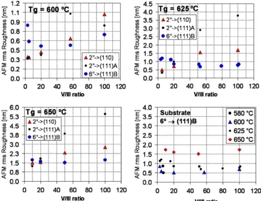
It is known that ordering in GaInP grown by metal organic chemical vapour deposition (MOCVD) depends on the growth conditions and substrate misorientation. Some general trends have been found for the relation between a growth parameter and the ordering achieved[4]. However, the interrelation between the growth parameters and the ordering is intricate, and a tendency, observed for a given set of growth parameters can change when modifying any of them.
In this work, a number of experiments are performed in order to determine the ordering level in GaInP for a set of growth conditions and GaAs substrates. The semiconductor structures used for the study consist of 300 nm thick undoped GaInP layers lattice matched to GaAs grown on top of 250 nm thick buffer layers. Growth temperatures from 580 to 6501C and V/III ratios from 2 to over 100 are explored, for three different substrate
misorientations. The growth rate was kept constant at 1.5
m
m/h. The cooling down of the sample was done under a TBP stabilized atmosphere. The assessment of the ordering is made in terms of the absolute difference between the band gap of the GaInP test layers at room temperature, and the band gap of a completely disordered GaInP material, whose value at 295 K was taken to be 1.91 eV for the GaInP lattice matched to GaAs[6]. The (optical) band gap of the test layers was estimated using RT-PL. The value obtained was then corrected for the observed small composition deviations from the lattice matched to GaAs one, measured by HRXRD[7]. The surface morphology is characterized using AFM. A summary of the experiments is presented inFigs. 1 and 2. Some relevant conclusions for our purposes drawn from the data can be summarized as follows: For all temperatures and substrates, the ordering increases when the V/III ratio is increased, more pronouncedly for values below 20. The maximum ordering is achieved with 61-(111)B sub-strates at 6501C and V/III4100. The maximum variation of the ordering changing only the V/III ratio (50 meV) is achieved with 61 -(111)B substrates at 6251C. The roughness increases as temperature increases, for all the substrates. The dependency of the roughness with the V/III ratio is minimum with the 61-(111)B substrates. For V/III ratios from about 20 to higher values, the minimum roughness is achieved with 61-(111)B substrates.presumably coming from the fact that wafer pieces of different sizes were used for each experiment and they were positioned in a slightly different part of the 200 recess of the satellite during
growth.
The aim of the GaInP layers grown at 5801C and low V/III ratio was to achieve the most completely disordered layer possible. It is observed that the absolute band-gap energy difference of such a layer is about 7 meV. An attempt to further decrease this value by decreasing the V/III ratio gave rise to a GaInP layer of such a bad morphology that it appeared milky to the naked eye. Thus, the layers grown at 5801C and a V/III ratio of about 7 were considered as the less ordered layers achievable in the range of growth conditions explored.
4. GaInP concentrator solar cells grown with ordered GaInP and a BSF based on an order–disorder heterostructure
After the results obtained in the previous experiments, the substrates oriented 61-(111)B were considered more appropri-ate for the growth of solar cells based on ordered GaInP for the active layers and on an ordered–disordered heterostructure used as the BSF. On the one hand, the ability of achieving a highly ordered layer and the widest band gap difference is advantageous for the growth of the BSF layer based on an ordered–disordered heterostructure. On the other hand, the surface morphology studies suggest that 61-(111)B oriented substrates are the most flexible in terms of roughness at different growth temperatures and V/III ratios.
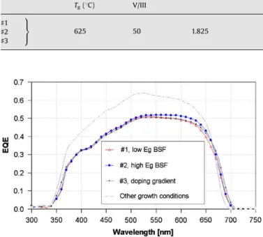
The structure of the solar cells grown is shown inFig. 3. The values chosen for the active layers thicknesses and doping levels are the standard ones that produce high efficiencies in multi-junction solar cells[3,5]. As for the growth conditions they were chosen keeping in mind the tradeoff imposed by the ordering necessary in the active and BSF layers to be able to produce an sufficient conduction-band discontinuity to serve as an effective
reflector for minority carriers (holes), and the quality of the photoactive layers, i.e., the emitter and base. Three structures were grown and a summary of their growth conditions can be found inTable 1. The conditions chosen for the active layers also appear to be the optimum to achieve a good electronic quality, since the surface roughness is minimum and the RT-PL peak intensity was in the range of the highest values (not shown here for brevity).
The solar cell structures were then processed into concentrator solar cell devices with 1 mm2active area and an inverted square
front grid. The quality of the semiconductor structure was assessed by way of the analysis of the EQE of the device. The curves obtained are shown in Fig. 4. The EQE of another GaInP solar cell with similar thicknesses and doping levels but grown with PH3as group-V precursor and at different temperatures and
plotted for comparison purposes. Since the GaInP compositions obtained with HRXRD showed to be quite close, the difference in ordering level is deduced directly from the absorption cut-off wavelength in the EQE, which is higher in the case of more ordered material. About the BSF quality, the differences between the three structures grown are clearly noticeable. The structure with the higher conduction-band discontinuity produced by the highly disordered BSF layer (]2) shows the best response in the lowest energy region, which can be ascribed to a more effective reflection of the minority carriers. The behavior of the BSF layer generated with a change in the V/III ratio from the BSF to the base layer is not better than that of the BSF created with a doping level gradient. This is consistent with the data presented inTable 1. The difference of just 35 meV between the band gap of the BSF and base layers, clearly below the minimum 2 kT value necessary to serve as an effective minority carrier barrier, explains the worse performance of this BSF layer.
The low amplitude of the EQE of the solar cells grown in this study is remarkable. This affects directly the short-circuit current of the solar cell. The worse response in the solar cells grown with more ordered GaInP is believed to be due to poor minority carrier properties of this material. In fact, the simulations carried out using the Hovel model [8] give rise to very close fits of these curves if very low minority carrier lifetimes or mobilities (i.e. low diffusion lengths) are used in the calculations. The origin of these poor minority carrier properties cannot be blamed on structural defects coming from an excessive lattice mismatch, since the HRXRD measurements showed a
D
a/avalue below 7.5105. Theuse of TBP, which in the past was found to be problematic in obtaining phosphide materials with high minority carrier proper-ties [9], is nowadays improved to an extent that makes it appropriate for growing high-quality material [10]. Moreover, oxygen, carbon and atomic hydrogen SIMS profiling performed on the samples grown in this study (see Fig. 5) show a residual
concentration of all these elements very similar in the solar cells grown with PH3and TBP, and with quantities below any harmful
value. Thus, the use of TBP itself does not appear to be the origin of the poor minority carrier properties found. On the other hand, the ordering in GaInP is known to produce a reduction in the electronic quality of the GaInP layers due to the formation of traps arising from the order/disorder domain matrix [11]. However, other sources of the poor electronic quality like native defects due to the growth conditions chosen cannot be discarded. A deeper study of the causes falls out of the scope and length of this paper, but it is currently being studied.
The solar cells fabricated are aimed to work under concen-trated light. However, the standard EQE measurements are carried out at low- light densities, much below the 1 sun equivalent (in our case it is as low as 1/20 suns). In some cases, it has been found that the EQE response improves if a light bias is applied to the solar cell during the measurement[12]due to the saturation of the recombination centers that worsen the response of the solar cell. To study this effect on the solar cells we are analyzing in this work, a 635 nm laser light bias equivalent to the irradiance of 7 suns was applied to the solar cells during the EQE measurement. Table 1
Growth details of the GaInP solar cells grown
Run Photoactive layers growth
conditions
Photoactive layers nominalEg(eV)
BSF layers growth conditions BSF layer nominal Eg(eV)
Base-BSFEg
difference (meV)
Tg(1C) V/III Tg(1C) V/III
]1 9>=
>
; 625 50 1.825
625 3 1.860 35
]2 580 7 1.903 78
]3 625 50 (mdoping) 1.825 0
Fig. 4.External quantum efficiency of the GaInP solar cells fabricated. The EQE of a similar solar cell with less ordered GaInP and grown with PH3 is shown for
comparison.
The result for one of the samples is shown inFig. 6. For the other samples, the result is similar. The important improvement in the EQE can be seen, which supports the idea of a trap related poor EQE performance. In the improved EQE curve, a higher improve-ment in the response for high photon energies can also be appreciated. This is due to the laser light wavelength used, with which the excitation is higher in the upper layers. Although it is necessary to study more in depth the characteristics of the traps involved, it appears that they may not be necessarily a problem for the solar cell performance when working under concentrated light.
5. Summary and conclusions
In this work, the relation between growth conditions, ordering and surface morphology for different substrate misorientations have been studied. For the V/III ratio and temperature ranges explored, it has been found that the 61-(111)B substrates allow the maximum variation or ordering changing only the V/III ratio. These susbstrates also show the minimum surface-roughness sensitivity to the growth conditions. The minimum ordering with this substrate was obtained at a growth temperature of 5801C and a V/III ratio of 7. This highly disordered layer was used as a BSF in a GaInP concentrator solar cell. The EQE result show an improved performance of this BSF with respect to other ones based on a doping gradient or a more ordered GaInP layer. The electronic quality of the active layer in the solar cells fabricated was found to
be poor, compared to other solar cells grown with PH3and a less
ordered GaInP. The SIMS measurements performed appear not to point to TBP as the origin of this problem. On the other hand, the traps causing the bad electronic quality are thought to come from growth native defects or the order/disordered domains matrix, although the exact origin remains to be determined. From the concentration EQE measurements performed, it was found that the electronic properties were improved with the light bias applied. The trap saturation is thought to be the origin of this behavior. Thus, it can be concluded that the traps introduced by the ordering in the GaInP are not necessarily a problem for the conversion efficiency when the solar cells are aimed to work at high concentrations. The particular characteristics of these traps are currently being studied.
Acknowledgements
This paper has been supported by the European Commission under contract SES6-CT-2003-502620 (FULLSPECTRUM project). The SpanishMinisterio de Educacio´n y Cienciahas also contributed with the CONSOLIDER-INGENIO 2010 program by means of the GENESIS FV project and also with the research projects with references TEC2005-02745, TEC2004-22300-E, and TEC2007-29630-E as well as theComunidad de Madridunder NUMANCIA program (S-505/ENE/0310).
References
[1] A. Gomyo, K. Kobayashi, S. Kawata, I. Hino, T. Suzuki, T. Yuasa, J. Crystal Growth 77 (1986) 367.
[2] Y.S. Chun, H. Murata, I.H. Ho, T.C. Hsu, G.B. Stringfellow, J. Crystal Growth 170 (1997) 263.
[3] R.R. King, et al., in: Proceedings of the Fourth International Conference on Solar Concentrators, 2007, p. 8.
[4] J.M. Olson, et al., in: A. Luque, S. Hegedus (Eds.), Handbook of Photovoltaic Science and Engineering, Wiley, 2003 (Chapter 9).
[5] K.A. Bertness, A. Sarah, R. Kurtz, D.J. Friedman, A.E. Kibbler, C. Kramer, J.M. Olson, Appl. Phys. Lett. 65 (1995) 989.
[6] M.C. Delong, et al., Appl. Phys. Lett. 66 (1995) 3158.
[7] C.P. Kuo, S.K. Vong, R.M. Cohen, G.B. Stringfellow, J. Appl. Phys. 57 (1985) 5428.
[8] H.J. Hovel, J.M. Woodall, in: Proceedings of the 10th IEEE PVSC (1973) p. 25. [9] R.W. Hoffman, N.S. Fatemi, D.M. Wilt, P.P. Jenkins, D. Brinker, D.A. Scheiman, in: Proceedings of the 24th IEEE PV Specialists Conference IEEE, Waikoloa, HI, USA, 1994, p. 1882
[10] H.-J. Schimper, Z. Kollonitsch, K. Mo¨ller, U. Seidel, U. Bloeck, K. Schwarzburg, F. Willig, T. Hannappel, J. Crystal Growth 287 (2006) 642.
[11] S.F. Yoon, K.W. Mah, H.Q. Zheng, P.H. Zhang, J. Crystal Growth 208 (2000) 197. [12] I. Garcia, I. Rey-Stolle, B. Galiana, C. Algora, in: Proceedings of the Fourth