Mini data logger system
75
0
0
Texto completo
(2) 1 lndex 2 lntroduction ...............................................................................................4 2.1. Project Description ........................................................................................... 4. 2.2. Objectives ........................................................................................................ 5. 2.2. 1. General Objectives .................................................................................... 5. 2.2.2. Particular Objectives .................................................................................. 5. 2.3. Justification ....................................................................................................... 6. 2.4. Project's scope ................................................................................................. 7. 2.5. SWOT Analysis ................................................................................................ 8. 3 Theoretical Framework ............................................................................ 9 3.1. Controller Area Network (CAN) ......................................................................... 9. 3.1.1. lntroductory concepts ................................................................................. 9. 3.1.2. CAN Frame ................................................................................................ 9. 3. 1. 3. Synchronization .......... ... .. ................ ........... .......... .... .... .. ......... . .. ... ..... ..... 12. 3.2. Serial Protocol Interface (SPI) ........................................................................ 12. 3.2.1. lntroduction .............................................................................................. 12. 3.2.2. Operation ................................................................................................. 13. 3.2.3. Advantages.............................................................................................. 13. 3.2.4. Disadvantages ......................................................................................... 14. 3.3. Secure Digital Card (SO CARO) ..................................................................... 14. 3.3.1. SD Card protocols ................................................................................... 15. 3.3.2. Comparison with other storage systems .................................................. 16. 3.3.3. Electrical Configuration ............................................................................ 17. 3.4. File Allocation Table System (FAT) ................................................................ 18. 3.4.1. File systems.............................................................................................. 18. 3.4.2. FA T File system structure ......................................................................... 18. 3.4.3. Boot sector ............................................................................................... 19. 3.4.4. FA T Table and Mapping ........................................................................... 20. 3.4.5. Root directory ........................................................................................... 20. 3.4.6. Data region .............................................................................................. 21. 3.5. 4 4.1. DBC (CAN Data base Container) .................................................................... 21. DATroniC System ................................................................................... 24 lntroduction ..................................................................................................... 24. 2.
(3) 4. 1. 1. Hardware ................................................................................................. 25. 4.1.2. Software .................................................................................................. 28. 5. System Redesign .................................................................................... 32. 5.1. Hardware Redesign ........................................................................................ 32. 5. 1. 1. CAN Module and SO Card Module .......................................................... 33. 5. 1. 2. CAN Bus Synchronization and architecture ............................................. 35. 5.2. Software Redesign ......................................................................................... 37. 5.2.1. Programming Logic.................................................................................. 37. 5.2.2. lnteraction with the CAN bus ................................................................... 40. 5.2.3. DBC parser.............................................................................................. 43. 5.2.4. User interface .......................................................................................... 44. 5.2.5. General system function .......................................................................... 47. 6 General Proofs and Results .................................................................. 50 6.1. System Performance ...................................................................................... 50. 6.1.1. Test description ....................................................................................... 50. 6.1.2. Results .................................................................................................... 52. 6.1.3. System limitations .................................................................................... 55. 6.2. Sample rate tests ............................................................................................ 56. 6.2.1. Test Description ....................................................................................... 56. 6.2.2. Results .................................................................................................... 57. 6.3. System Validation ........................................................................................... 59. 6.3.1. Test Description ....................................................................................... 59. 6.3.2. Results .................................................................................................... 61. 7 Conclusions ............................................................................................ 64 7 .1. General conclusions ....................................................................................... 64. 7.2. Future work .................................................................................................... 65. Bibliography and References ..................................................................... 66 Appendixes ...................................................................................................67 Technical Training ................................................................................................... 67 AFT Hardware and Software ............................................................................... 67. Kvaser ..................................................................................................................... 68. User manual ................................................................................................. 71. 3.
(4) 2 lntroduction 2.1. Project Description. The Mini Data Logger is an automotive data acquisition and storage system capable of reading messages through a CAN bus and writing them in a SDCard. The purpose of the device is to connect itself to a CAN bus, acquire and store specific trames coming from the car and even from different signal acquisition modules connected to it, according to the user requirements. The company AFT Atlas Fahrzeugtechnik GmbH, AFT from now on, requested this project in arder to redesign ene of their products to have the capability of reading data from any automotive company, not only from a specific ene, and with a reasonable cost (company's current problem). The hardware to redesign is the DATroniC 3.0 available only fer Mercedes Benz trucks.. AFT is a company that develops vehicle electronics and is a specialist supplier of prototyping and series development; also, it has a range of expertise in mechatronics, measurement, calibration systems and vehicle acoustics. 1 Among all of their products they have the 4Measure, 4Log and DATroniC. The 4Log system is a device that can pe~rform all the requirements but the cost is the problem, so the Mini Data Logger will be the redesign of the DATroniC to achieve the performance of the 4Log.. lt is required that the new system is robust, versatile, modular, and above all, universal: any automotive company should be able to load their personal configuration to the device, acquire their desired signals and store them. This device will help the companies to make their data acquisition and testing process easily and efficiently without AFT direct intervention.. 1. Taken from http://www.aft-werdoh\.de aboutAFT. 4.
(5) ... @ DBCFlle. 11. Signa/. Signa/. S/flnalAc. Module. Figure 2-1: Graphical description of the ;:,roject. 2.2 Objectives. 2.2.1 General Objectives. •. Redesign the current AFT DATroniC Systern to make it capable of acquiring data from multiple automotive companies and different signal acquisition modules, and store that informatio11 in a SD Card for future analysis and use.. •. Create an easy-to-use interface to specify a DBC file to be read and create the necessary files to program the Mini Data Logger System.. •. lntegrate the new device and software as part of a modular data acquisition and storage system.. 2.2.2 Particular Objectives. To make the design process efficiently, the project was divided into hardware and software. Each area's particular objectives are described below. Hardware: • Design of a SD Card module using the expansion ports in the. DATroniC core.. 5.
(6) •. Add a 9 pin connector far a new CAN bus to be used with the 4Measure modules.. •. Physical construction of the prototype far analysis, future improvement and space requirements of the company.. Software: • Enable a new CAN module.. •. Filter the desired signals.. •. Save and load files from a SD Card. •. Store and read files using a FAT file system.. •. Universal interpretar of DBCs. •. Create a friendly graphic user interface to. •. Store all the desired signals in an easy to read text file.. USE!. the interpretar.. 2.3 Justification Automotive manufacturers require effective testing solutions, which can often become too expensive due to today's data acquisition systems far CAN Protocol are very specific. By designing and building a device that is more versatile and universal, you can get lower costs as the entire testing architecture becomes more efficient.. Advantages from the Mini Data Logger versus DATroniC: •. Universality: Can load different configurations from any company using only its CAN database (DBC file).. •. Do not need of a connected PC while logging data.. •. lt can lag the data received via CAN bus in a SD Card.. •. lt has compatibility with 4Measure modules in an independent CAN connector.. •. In system interpretation: The data is written in a plain text file with a farmat easy to be read by the user. lt is done in run time, not in the PC.. Advantages from the Mini Data Logger versus other products in the market:. 6.
(7) •. Low cost: Comparing the price of the 4Log system, the Mini Data Logger is a lot cheaper and it can achieve good results in tests where a few of signals are needed to be monitored.. •. Easy configuration: Using a graphic user interface the module can be configurad, only needing two buttons to start using the system for tests.. •. Low energy consumption: comparad with other testing systems the Mini Data Logger uses less energy. Compamd with the 4Log system.. •. 2.4. No PC needed for data log, comparad with the Kvaser Memoratum.. Project's scope. lt is expected that the redesign of the DATroniC System can be optimizad so it can correctly read and log signals at high sample rates: for the CAN Bus, it is expected that the systems logs data for all data acquisition modules, so it can be competitiva in the automotive industry. There should be also a detailed analysis of the limits of the system: the maximum amount of channels, baudrate and modules that can be used at the same time without losing information. The user interface should allow the user to easily load their configuration file (according to each company's requirements) and set different parameters for their measurements. This interface should be as easy to use as possible. The final result will be an optimization of the current system, with a detailed analysis of the limitations and further development opportunities for the system.. 7.
(8) 2.5. SWOT Analysis. Strengths. -. Most if the hardware is already. -. the beginning, so severa! parts. Module and the CAN. of tht~ code will be unknown.. -. desi~1ner will not always be. programming and testing.. possible.. The project has the support of. -. Communication with people of. people from the company and. Germany will not be as. from the student that made the. complete as it should because. last Phase.. of time constrains. The code has flaws that can. Threats. -. The system has sorne. be corrected in arder to get a. hardware limitations that will. better performance of the. limit the scope of the project.. system.. -. Collaboration with the re-. so most of the work will be on. Opportunities. -. Programming will not start from. made (only the SD Card. connector have to be added),. -. Weaknesses. -. Time constrains. Possible optimization of the code can be made from AFT people.. -. The current interface can be improved to meet user's needs. 8.
(9) 3 Theoretical Framework 3.1. Controller Area Network (CAN). 3. 1.1 lntroductory concepts The Controller Area Network (CAN) is a communication protocol based on serial bus topology suited for intelligent devices within a distributed system or sub system with real-time capabilities. CAN protocol uses the producerconsumer concept and these are sorne of its main features: •. Message priority. •. Configuration flexibility. •. Data consistency. •. Multi-master system. •. Error signaling and detection. •. Automatic retransmission of wrong frames. •. Low latency times. The multi-master capability, one of its main features, means that all nodes within the CAN bus can transmit or request data simultaneously. A transmitting node will broadcast a message, but only interested listeners will receive the information. The CAN Bus can get a speed of 1Mbit/s for short distances and also have the advantages of bein~1 of low cost, easy-to-use, suited for rough environments and has power reduc:tion capabilities.. For these advantages, CAN protocol has been a.dopted by the automotive industry as its main protocol for communication. CAN Protocol works mainly in three layers of the OSI Model: Application, Data Link and Physical Layer. [3] 3.1.2 CAN Frame. 9.
(10) O to 8 Byte 16 Bit 2 Bit. 1 Bit 12 or 32 Bit. 7 Bit. 3 Bit. Figure 3-1: CAN Frame. The figure above shows the main structure. ot the CAN trame.. As said before,. the CAN Bus manage different priorities so it two trames are traveling through the bus at the same time, both will remain active until one is tound to have one dominant bit and the other a recessive bit at a certain point. ot the trame.. The trame with the dominant bit will remain in the bus while the other will be discarded. Each. ot. the fields within the trame will be explained in greater. detail.. Arbitration Field:. Standard Frame Format Control Field SOF 11 bit ldent1trer. IDE. ro. - Data Field -. DLC. Extended Frame Format - - - - - Arbitration Field - - - · - - - Control Fie. r1 ro DLC Figure 3-2: Arbitration Field. This part. ot the trame. contains the identifier, which can be. ot. 11 or 29 bits,. depending on it it has a standard or extended format. The RTR field reters to the Retransmission Request and it is sent as a dominant bit when the trame is a Data Frame, there also exist Remete Frames which are sent to request the retransmission. ot information and its RFR field is sent as recessive.. Control Field:. 10.
(11) Figure 3-3: Control Field. The Control field main purpose is to describe the length of data contained in the data field of the trame. The DLCO to DLC3 are 4 bits to indicate the number of bytes in the Data Field. A combination from O to 7 indicates a data field from O to 7 bytes. AII other DLC combination indicates a data field with 8 bytes from which combinations from 9 to 15 can be used for any special function. The IDE Field refers to the identifier extension, which is sent dominant in a standard frame and recessive in an extended trame (this means that a standard trame will always have greater priority than an extended one ).. Data Field:. ·,_,Byte·f .· :e· ···e:2·.··:ayt~~·; g,Je,\ .a.···.yt ,yt···.e.·i.6 s ..··,lh=>_·: .· ·.e!' . .)" :a_, ' . ·. ·e:t• ..,.•· . r·· ·.e·a···.1· ·r.'.· ' . . ' .Yt. ' . ' . .. .. . ',.,. ~' . . 1 · _··, ·yi_··· .. B .• _. V. ·· ·.s. ·. ·. ... •. ;. • · •··. ". .. . .. ··. min. length of Data Field = O Byte. max. length of Data Field = 8 Byte Figure 3-4: Data Field. The figure shows the distribution of the data frame. There are sorne trames that can include no data at all and still transmit information (through the ID of the frame).. CRC and Acknowledge Field:. The cyclic redundancy check and the acknowledge field are used to ensure the consistency of the whole message. CAN Protocol has several methods to ensure a correct transmission.. 11.
(12) 3.1.3 Synchronization. In a CAN bus for a communication to begin all the devices must be configured with the same baud rate. lt one ot the devices is out ot sync error trames are sent to the bus so the communication is interrupteid. The devices can be in normal operation or in silent mode, the last one is used as a sniffer in the CAN bus and only send recessive bits as response. In this case the device in silent mode will not be visible for the other devices in the bus so it it loses synchronization, error trames will not be sent. [3]. 3.2. Serial Protocol lnteñace (SPI). 3.2.1 lntroduction The Serial Peripheral Interface Bus is an asynchronous serial data link standard named by Motorola that operates in tull duplex mode. Devices communicate in master/slave mode, where the master device starts the data trame transmission. The SPI bus specifies tour logic signals: •. SCLK: Serial Clock (output trom master). •. MOSI: Master Output, Slave Input (output from master). •. MISO: Master Input, Slave Output (output trom slave). •. SS: Slave Select (active low, output from master). Figure 3-5 SPI Bus Signals. 12.
(13) 3.2.2 Operation The SPI bus can operate with a single master device and with one or more slave devices. Most slave devices have tri-state outputs so their MISO signal becomes high impedance ("disconnected") when the device is not selected. Devices without tri-state outputs can't share SPI bus segments with other devices. In single slave mode, only one slave can talk to the master, and only its chip select could be activated. To begin a communication, the master first con·figures the clock, using a frequency less than or equal to the maximum frequency the slave device supports. Such frequencies are commonly in the range of 1-70 MHz The master then pulls the chip-se/ect pin to low for thi~ desired chip. lf a waiting period is required (such as for analog-to-digital ccmversion) then the master must wait for at least that period of time before starting to issue clock cycles. During each SPI clock cycle, a full duplex data transmission occurs: •. The master sends a bit on the MOSI line. •. The slave sends a bit on the MISO line. Master 1. Memory. I o! 1! 213141 si 6171. t. Slave 1. .... SCLK ... MOSI. 1. l.llemory. 1. ~0ilil 3l 4 l 5 l 6l 71. MISO. 1. Figure 3-6 Full Duplex Operation. Transmissions may involve any number of clock cyc:les. When there is no data to be transmitted, the master stops toggling its clock; then it deselects the slave. Every slave on the bus that hasn't been activated using its chip select line must disregard the input clock and MOSI signals.. 3.2.3 Advantages •. Full duplex communication. •. Higher throughput than l2 C or SMBus. 13.
(14) •. Complete protocol flexibility far the bits transferred. •. Not limitad to 8-bit words. •. Arbitrary choice of message size, content and purpose. •. Extremely simple hardware interfacing. •. Typically lower power requirements than 12C or SMBus. •. No arbitration or associated failure modes. •. Slaves use the master's clock, and don't need precision oscillators. •. Slaves don't need a unique address -- unlike 12C or GPIB or SCSI. •. Transceivers are not needed. •. Uses only tour pins on IC packages, and wires in board layouts or connectors, less resources than parallel interfaces. •. At most one "unique" bus signal per device (chip select); all others are shared. 3.2.4 Disadvantages •. Requires more pins on IC packages than l2 C. •. No hardware flow control by the slave. •. No hardware slave acknowledgment. •. No error-checking protocol is defined. •. Generally prone to noise spikes causing faulty communication. •. Only handles short distances compared to RS-:232, RS-485 or CAN-bus. SPI was the chosen protocol far its capability of cornmunicating in an efficient way with the SD CARO.. 3.3 Secure Digital Card (SD CARD) The Secure Digital (SD) Cards are removable storage devices based in nonvolatile flash memories. Today, these devices are used widely in the market, especially in cameras, PDA's and portable devices. They were first introduced by Panasonic and were developed as the evolution of the Multimedia Card (MMC). Nowadays, companies such as Toshiba, SanDisk and MEI produce the SD cards. There have been sorne evolutions such as the MiniSD and Micro SD.. 14.
(15) The SD cards can be of different classes, each one1 having a different transfer speed and storage capacity, as shown in the following table:. , Class. o 2 4. 4MB. 6. 6MB. 10. 10 MB. Table 3-1 SD Carel Classes. The SD card manages a file system that helps interpreting stored data, FAT16 or FAT32, having compatibility with almost all existing operating systems.. 3.3.1 SD Card protoco/s The SD cards can communicate vía three different protocols, two SD protocols and SPI:. •. SD protocol - consists in a synchronous serial protocol with ene ( 1-bit protocol) to tour data lines (4-bit protocol), ene clock line anda command line working in a master-slave scheme with a 16 bit Cyclic Redundancy Check (CRC) fer error detection.. •. SPI protocol. The SD communication has a command-respons,e architecture, the master sends all the commands and wait fer a response from the slave that indicates start of a transfer read or write, or with an error message. The master commands are sentina format "CMD-XX" or "ACMD -XX", depending if it's a general command or an application command, respectively.. The master packets are sent in a 7-byte trame as follows:. 15.
(16) I O 11 16-bit Command I Argument (MSB first) 2-5 bytes I CRC - 7 bits 11 1 Figure 3-7 SO Card Packet. First Byte - lnit Byte 2 - 5 Bytes: Data stream Last Byte: Error detection and end of frame. The slave has three types of response depending of the command read, but the most general response is a one byte response that indicates the most important and common errors that happen in the communication.. I B yte I Bit 1 ::vleaJllng l. 1 6 5 4 3 2 1. o. Start Bit, Always O Parametér Erroi· A<l<lress Error Erase Sequeuce Errút CHC Enor lile-gal CO!lllll8.ll<l Era...e Heset In Wle 5tate. Figure 3-8 SO Card Response. lt can also make bulk data transfers to move lar~1e amounts of data. lt can send data streams of any size, the most common is 512 bytes (the size of a FAT cluster). lt works the same as the command-respond, but it has a start of block token ("11111110") and an end of block token ("XXXOAAA1" X: Don't Care, A: Status - "01 O" correct Data; "11 O" - failed to write data"). [2] lf a block read fails, a byte is sent with the error found: 1 B it 1 Meaultig 1 Always 'fl'. 6 5 4 3 2 l. o. Alwa.ys '()' Alwa.ys 'ff. Ca.ni Laclw<l Out of H.8.llge Carel ECL Fe.iJed.. Cru:rl Cautroller Error l,,"i.ispecified Error Figure 3-10 SO Error Found. 3.3.2 Comparison with other storage systems. 16.
(17) Size - 32 mm x 24 mm- lt is better than USB pen drives. The interface (communication and init of the module) it's less complex than USB and Compact Flash (CF). The SO shows better performance when there is an interface complexity concern (in our project it's a concern). The supply voltage and current are less demanding than the CF and USB devices using a supply voltage of 3.3 V and a supply current: 20mA - 1OOmA. Also, it is important that the power consumption must stay low. (Being the OATroniC a traveler module, mínimum power consumption is required).. 3.3.3 Electrical Configuration. The physical structure of the card has 9 wires to communicate with other modules, in the figure 3-9 all the connections neede!d to work with the SO card are shown. The functions of each pin will be explairied in the table 3-2:. ~''~'''ij' • Figure 3-9 SD Carel Structure. Pin. SPI Mode. SO Mode. 1. Slave Select (SS). Data Une 3. 2. Master Out Slave In (MOSI) Command Une • Ground. Ground. 6. Ground. Ground. 7. Master In Slave Out (MISO). Data Une O. 8. IRQ. Data Une 1. 3. 4 5. 17.
(18) 9. Unused. Data Une 2. Table 3-2 SD Card Electrical Connections. 3.4 File Allocation Table System (FAT). 3.4.1 File systems lt's a mean to organize and control data in a storage system in an efficient way, to make the best use of space and to manage data in a reliable way to avoid losing infarmation. Without a file system, the software loading a file must know where are located all the parts of the file and its exact size; also, to save a file it must be aware of all the available space and its location. [2]. File systems appear far the need of storing files, have reliable data, storage systems independent from the main system, saving program memory, make a generic use of the storage devices by any software and the OS. Among the most important file systems, there are FAT and NTFS far the Windows OS. The most important functions that a file system must have are reading and writing files. They also need to have the capability of searching a specific file in the storage systems; provide protection of infarmation with the possibility of read-only and rewritable features; have free-space management and logic organization of files in the storage device by using IDs and file extension far its later execution.. 3.4.2 FA T File system structure The File Allocation Table (FAT) is one of the first file systems to appear in the market, being the first one of 12 bits evolving to 16 bits and the most widely used: the 32 bits version (FAT32). This file system appears to salve the problem of file managing in the floppy disks in DOS and Windows OS, but its robust structure makes it still usable nowadays. lt's one of the quickest and most compatible file systems in the market to use in memory-cards. This is one of the most important reasons for its use in this project.. 18.
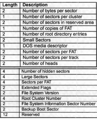
(19) The structure of any FAT file system has four parts: Boot Sector, the File Allocation Table, the root directory and the data region ar clusters. The boot sector is the most important of the three because it is where the BIOS parameter block is located, which specify the size of the FAT and the clusters. FAT contains the arder in which the parts of the file are in the data region; the root directory its where the name of the file is and also where is its data located; and the last section is the data region where all the bytes of the file are. [2]. 3.4.3 Boot sector The boot sector has 512 bytes long and it's conformad by: Length 3. 8 53. 26 420 2. Description Jump instruction OEMID BPB Extended BPB Bootstrap Code End of Sector Marker. Figure 3-10: Boot Sector. The most important block of this sector, the BPB (Bias Parameter Block) is where the size of each sector is located, and also describes how many bytes are per sector, the sectors per FAT, number of FATs, reservad sectors and number of root directory entries. The distribution is as follows:. 19.
(20) Oescription. Length 2 1 2 1 2 2 1 2 2 2. Number of bytes per sector Number of sectors per cluster Number of sectors in reserved area Number of copies of FAT Number of root directory entríes Small Sectors DOS media descriptor Number of sectors per FAT Number of sectors per tracl< Number of heads. 4 4 4 2 2 4 2 2 12. Number of hidden sectors Large Sectors Sectors per FAT Extended Flags File System Version Root Cluster Number File System lnformation Sector Number Backup Boot Sector Reserved Figure 3-11: FAT Description. 3.4.4 FA T Table and Mapping The FAT table has the mapping of the data stored and its size is variable based on the storage capacity of the device. The number of FAT tables makes the storage in the device robust and reliable; if one FAT fails to be read, the copy can be used to recover the information. The entries in the FAT are decided by the number that it has, if its zero is an available cluster; other number means that is used for reserved operations or it has the location of the next cluster of information.. 3.4.5 Root directory In this sector are all the attributes of each of the files stored. lt contains the name of the file, attributes (read-only, rewritable, directory, etc.), size of the file, first sector of file in the FAT table and data region, and the date of modification. The distribution of the bytes works as shown in the figure 3-12:. 20.
(21) -/. Allrit!utN. ~· 11 1. '\. 8equenc8. Sec. 1 1 1. 10 Sella-. I lo! 1. -/ /. t.. t. Upper 111 bis. ar ..ana. LoMr 16 bils af llarlng. blodl. blod(. 12 lldllnclln. 4. 2. 1° 1--I 2. Figure 3-12: FAT Bytes Distribution. The bytes distribution in the upper figure refers to the short name and the other refers to a long name file. The short name clistribution of bytes is used with file names of eight or less characters and it has compatibility with the 16 bits version. This type of distribution always starts with a letter and the entire name is in upper case. The long name distribution always starts with a number, which represents the sequence of entries in which the entire file name is contained. Based on this information, the search of a file in the data region is established.. 3.4.6 Data region lt's the sector with the most space of all; files data are distributed here and are recove red when the read function is called.. 3.5 DBC (CAN Database Container) A DBC file is a recommendation to standardize and specify the messages that a user wants to retrieve from the CAN bus. In industry the DBC files are used to have control over their products so they can be easily tested. lt also includes many parameters necessary for the correct interpretation of each signa l.. 21.
(22) VERSION "DNNBNNNYNN ...NNNNNNNNN/4/%%%/4/'%**4NNN///" NS_: NS_DESC_ CM_ BA_DEF_. BS_: BU_: DME DGS DIS ... BO_ 1288 DME_l: 8 DME SG_ N_MOT: 0116@1+ (0.25,0) [0132767] "1/min" DGS DIS SG_ N_AB: 0116@1+ (0.5,0) [0132767] "1/min" DGS DIS. Figure 3-17 Example of a DBC FilEi. Tags meaning: Tag. Meaning. VERSION. Is always the first line of any DBC file. lt's a string of 40 characters representing the file version.. NS:. Section with the additional key words used in this file.. BS_:. Beginning of the message section. BU:. Sender and transmitter declaration (Optional). 80_. Message definition. SG-. Signal definition. Message definition: Tag. ldentifier. 80_ 1288. B0_ 1288 DME_l: 8 DME. Message name. Number of bytes transmitted. Sender. DME 1. 8. DME. The most important field in this definition is the identifier/priority number and the number of bytes to be read in each transmission. lf the identifier happens to have extended format, the number will be: (2 32 -1) - ID value.. Signal definition:. SG_ N_MOT: 0116@1+ (0.25,0) [0132767] "1/min" DGS DIS. Tag. Signal name. Start bit. Length [bits]. Format. (Un)Signed. SG-. N_MOT. o. 16. 1. +. 22.
(23) Factor. Offset. Min. Max. Unit. Receiver set. 0.25. o. o. 32767. "1/min". DGS DIS. •. The length of a signal can vary from 1 bit to 32 bits. Therefore in a single CAN frame the max number of signals to be read is 64.. •. The format can be O (Motorola / Big Endian byte arrangement) or 1 (lntel I Little Endian byte arrangement).. •. The value can be signed (-) or unsigned (+). In case it is signed the leftmost bit represents the sign.. •. The factor represents the weight of a bit step. The value of the least significant bit.. •. The offset is the value it has to be added to reach the mínimum value. lt is generally used when the value is unsigned so it can reach negativa values.. •. Min and max, as their names say are the limits in which the signal can vary.. •. The unit is used only to know what is measured. lt can be empty, but is recommended be used.. •. The receiver set is only used if a sender and transmission declaration were made before. In any case it is also optional.. 23.
(24) 4 DATroniC System 4.1. lntroduction. The DATroniC is an embedded data logging system designed for acquisition and logging of automotive control signals ranging from temperature measuring to tachometer events registration. Data is acquired and gathered through two CAN buses. In addition, the DATroniC is capable of interfacing through USB, Bluetooth, Ethernet and driving a GSM module for geo-location data in route tracking applications. The complete system may be summarized as a set of peripheral controllers, connectors and memory chips controlled by a 16-bit microcontroller running on a Real Time OS for task administration and c:ased in a high resistance aluminum case.. The DATroniC was made specially to work with Mercedes Benz trucks so it has a very specific data acquisition made only to fit the requirements of the company. The program loaded to it is so selective that it has to be configured for each truck and only the signals that were important for them. Also it has to be connected to a PC to show all the data that has been acquired.. Figure 4-1 DATroniC System. 24.
(25) 4.1.1 Hardware Microcontrol/er Processor Unit. The DATroniC uses a MC9S12XDP512 16-bit Freeiscale Microcontroller with a 144 pin-out distribution featuring SPI and CAN buses for interfacing with system peripherals and memory banks. lt includes a lot of other features including analog-digital channels, PWM generators, timers, interna! memory, parallel digital outputs/inputs, and serial channels communication. The reason this MCU is used is that it also has a peripheral co-processor included that can handle the CAN bus while the main processor is used in other task. [9] Control-Input. The DATroniC microcontroller operates at loWE:lr voltages than signa Is received from the outside so additional conditioning is necessary in order to get them into the controller without damaging it. This voltage reduction circuits includes a voltage step down regulator, filters, etc. Also there are sorne special connections driven into the microcontroller with the ability to wake it up from sleep mode when change is detectad. MemoryBank. Although the DATroniC microcontroller has a certain amount of memory, it is not enough to manage all signal data storing and manipulation processes so memory banks are created to extend the system's capacities. RAM (2M x 16 bit) and Flash (2M x 16 bit) memorias have been added to increase data manipulation and storage respectively. The communication with the memory banks is done through parallel input/output digital ports. Bluetooth. A Bluetooth module is included in the DATroniC allowing wireless pairing and communication. Parallel input/output digital ports control the module. Data streaming is sent and received through serial port microcontroller peripheral.. usa. 25.
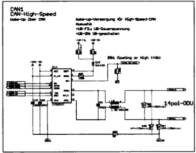
(26) A USB port is available far interfacing, data transfer, and configurations programming.. USB is interfaced through. an. FT232 chip far direct. communication by serial microcontroller peripheral.. GSM. GSM module support is being implemented in software and ready-to-go on hardware design; however, the module is not shipped by default with the system, instead, there are two female dip connectors ready far module's plugging-in purposes. GSM module is wired far multiple communication standards; 12C, SPI, and serial communication, module control is done through parallel input/output digital ports. CAN. lt includes a 14 pin connector that has 3 CAN inputs. Only 2 of them usable, one is a high speed connector at 500 kbps and the other is a slow speed CAN connector at 31.25 kbps. lt has an extra one the is not wired to the system that is also high-speed (500 kbps). This connector is the one that we will be using to implement the new module. Sorne schematics:. ---~-. CAN1 CAN-High-~d. .J1pol-OOU. Figure 4-2 CAN Module 1. 26.
(27) CAN2. CAN-Hiqh-SpNd. ~~E3:::!:=l=~. ~. _, aM.. Figure 4-3 CAN Module 2. CANi CAN-High-Speed. Figure 4-4 CAN Module 4. --!Gr---. ............................ ~- -~........·~+-t--,-Q,--,-._,..--,. Pb, Cllbat~ ----· ::.... ............. -. i 1. Figure 4-5 CAN Module 3. 27.
(28) Ethernet. An Ethernet interface is placed to achieve data transmission, control and configuration. Connection is achieved through a standard RJ45 jack and data streaming is controlled by a microcontroller peripheral. 4.1.2 Software The main program has all the initializations of the communication modules as it can be seen in the figure 4.2. After that the Real Time OS (RTOS) 2 takes control, the importance of having an OS is that thE3 main processor and coprocessor use the same memory bank, so sorne control is needed to access the variables in that memory bank. lf it runs straightway the data would not be consistent. The main resource to have control is using a "semaphore flag" to lock access from ene processor ar the other, but never both at the same time.. 2The Real Time Operating Systems are used when a task need to be done in an specific time. lt needs to be deterministic to fulfill ali the operations within the required time span.. 28.
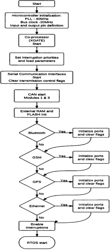
(29) Start. microcontroller initlallzation: PLL -40MHz Bus clock -20MHz Input and output pin definitlon. Co-processor (XGATE) Start. Set interruptlon prlorlties and load parameters. Serial Communication Interfaces Start Clear transmlsslon control flags. CAN start Modules 1 & 3. Externa! RAM and FLASH lnit. lnitlallze ports and clear flags. lnitlalizE• ports and clear flags. lnitializ., ports and clear flags. lnitializ,~ ports and clear flags. Enable interruptions. RTOS start. Figure 4-6: Flow chart of main prowam. 29.
(30) o. M Real Time OS. Transmit data ClearMCU. nags. Transmit data ClearMCU. Hags Sa.\!c coordina.tes and received time. t::: a,. .e. Read new configuration Flash overwrite. Transmit data Clear MCU flags. c.>. 3: o. Reload Timer. ,;::::. Nol. (/). ~. o:::. ¡;..:. ..,. ~. Transmit data Clear MCU. Hags. 5endstored data via Ethernet. :::, O>. u:. No. Lock semaphore Read acquired data from CAN bus Fill bulfers of data to be sencl Unlock semaphore Clear lOOms flag. Reload timer Reload timer. Send data via USB.
(31) The MCU is configured with a PLL to work at 40MHz with a source oscillator of 4MHz and a bus clock of 20MHz. The RTOS is capable of acquire the signals coming from the CAN bus every 1OOms and depending in which communication is enabled every 1O ms or 100 ms the data is sent to the PC. In the main loop of the MCU the device is polling if there is a new configuration to be loaded. This only consists in update the time and date; also can be updated via GPS if enabled to save datc:1. The figure 4-3 shows all the operations made by the main microcontroller in the RTOS. As it can be seen, all the tasks that need an specific time to be fulfilled are done controlled by timer routines, all of them used for data transmission or reception. So most of the load in the CPU is peripheral handling and polling for a new configuration to be loaded into the flash memory. And the least of the load is the interpretation of the data received from the CAN bus. This interpretation is rather quick because all of the received data has the same pattern, corresponding to the Mercedes Benz truck's DBC. Once the data is extracted and put in the corresponding buffer can be sent, but still is sent in raw format. The graphic user interface do the rest of the interpretation of this data, so the DATroniC can only work while it is connected to a PC/laptop that has the software, one flaw of this device. The CAN module is served by the coprocessor (XGATE) being attended by. interruption. routines.. Co-processor (XGATE) [. Each. module is configured at a different. No. baud rate. For synchronization the. <. time of bit is important so it is not too small, so even if it can achieve a No. <. 1MbiUs speed it is used at 500kbiUs using the oscillator as the time basis. In the figure 4-4 it's explained how. [. Lock semaphore. this works. Yes. Figure 4-8: XGATE flow chart. Unlock [. semaphore. 31.
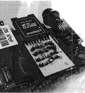
(32) 5 System Redesign To achieve our objectives, severa! changes have to be made on the system hardware and software. The current DATroniC System includes severa! features which will be removed to decrease the prize of the product while fulfilling its main function: acquiring CAN trames from the system bus and storing them in a SD Card which is easy to use for latl~r analysis of data.. 5.1. Hardware Redesign. First of all, our first approximation doesn't have to include a GSM, Bluetooth and the Ethernet Module (these peripherals increase the prize and are notas necessary according to AFT). This reduction frees sorne space, which can be used to insert the hardware for the SD Card. The following image describes the appearance of the front panel of the DATroniC a.fter these changes have been applied:. .r-.. PuW 10 Ei8<t CatQ. ~ E.. ,,o. ....... e. •. fll!l!li. ~. :>. www aft-vverdohl.de. ... Figure 5-1 New DATroniC Hardware. As shown in the image, the USB Port remains in its original place. The SD Card slot is added along with a new CAN connector, which will be compatible with other CAN connectors from other modules (such as the 4Temp)..
(33) S.1.1 CAN Module and SD Carel Module. The SPI channel O is available in expansion headers inside the DATroniC (header K6). This will help us make the interface with SD Card.. Figure 5-2 K6 Header includes SPIO. The new system will include several bridges, which will provide access to the CAN Frames received by one of the channels and will be send to the SPI Module for its later transmission to the SD Card.. DO!---=L...--~~~--+--+-' DII-----".__-~~-=----+--~. css 1-----';:____ GNJJ. _;u.1..k.:1..2.._. ___.. t----'~---,. SDCARD.t SDCARD_CON SDCard I MicraSD. Figure 5-3 CPU and SO Carel Connection. 33.
(34) To make use of the new CAN connector, the CAN4 module (high-speed and not wired in the original system) will be used:. CANi CAN-High-Speed •3U3 +5J. Spol-ODU C~i'. C~8. ql! 1.... "'·. ~. t: .-1. .......... TL..E62!186U33. ~g ". Ul'lll-1.20.S<n.b.). . ·····--·----·--····-··-··---··--·-····--···---·-···~,····--··---·OOND SGND3. Figure 5-4 CAN Module Connection. Here are sorne results of the system redesign:. Figure 5-5 Physical construction of the CAN Module. 34.
(35) Figure 5-6 Physical construction of the CAN Module. 5.1.2 CAN Bus Synchronization and architectum To be able to maintain synchronization with the CAN Bus with baud rates over 83.33 kbps, the system needs a new termination ( approximately 120 ohms) for the new CAN connector.. Figure 5-7 CAN Bus termination. 35.
(36) To connect more modules, the system made use of a T connector. This allowed the system to connect itself with the KvasE~r System that helped to make the acquisition modules' configuration. Figure 5-8 T Module. The final architecture of the data acquisition system is shown in the following image:. Figure 5-9 CAN Final Architecture. 36.
(37) 5.2. Software Redesign. As it has been said the Data Logger needs to have a communication vía CAN and SPI with the new modules; so besides the hardware each of the modules need to be implemented in this new design to fit with the specifications and to fulfill all the requirements. In this chapter all the software proposals will be explained using sorne function descriptions and flow charts.. 5.2.1 Programming Logic 5.2.1.1 Storage system. File manager. Fie AJlocationTable. SD-Card. Figure 5-1 O: Anatomy of storage system. SPI:. The SPI module is configured using the most common functions as init, send, enable and disable chip select. These functions are used as the core of all. data storage and SD Card control. The send function is used to read and write using the loopback feature that SPI has.. SO Card:. The SD card was implemented as a medium level library where all the functions are the least complex and high efficient. lt uses the block-data and frame-data to synchronize the SD Card with the micro-controller and store the data. The block-data send or receive 512 bytes per call as this is the common size of a FAT cluster in a SD card. The trame-data its structured to send. 37.
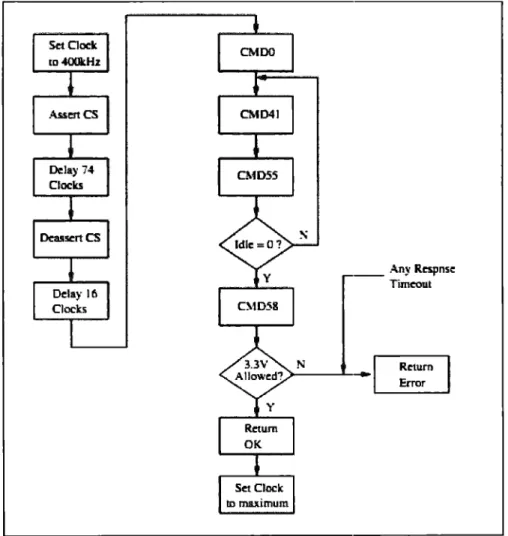
(38) commands to the SO card to specify the initialization, read or send operations of the card.. SD Card lnitialization:. The SD card initialization has a very particular way c,f work as it is needed to have compatibility among all the different classes and companies. The initialization process works as described in the figure 5-4:. Set Dock to.fOOkHz. _ _ Any Rcspnsc Timcout. >---J...·--~. ~. Set Cloclc ID maximum. Figure 5-11 SD card initialization flow cl"iart.. After all this steps the SD Card is ready to comrnunicate with the microcontroller and stays idle until another command comes. The next step it is to send a command to change the size of the data transfer to 512 bytes. After that it can read or write to any selected sector of the SD Card.. 38.
(39) To read, the CM017 (Read a single block) is sent, the slave sends a response followed by the start of block and then thei block-data is sent by it. As it is used with SPI then it's needed to send a 11umber of dummy bytes equal to the block size. To write a block a CM0:~4 is sent and after the response from the SO Card is received, the 512 bytes data can be sent. Even if the data is not 512 bytes wide, it is needed at least to send zeros to fill the spare space.. Other commands that were used in this project are the next enes: Cotun1aud C.:O.lDO L\1Dl6 C.\1017 01024 C.'.11)55 C),11)56 AC.'.ID41. Arguw.ént. Desc.ript lon. :\"one. Tell the caro to re.set and euter ils idle ¡tate. :,elect the block length . Head a s.iug!e block.. :l2- bit l:llock Lengt!J .12-bit JJlock Address 32-bit illocl...: Address. .\'one :'-01!€. .\"oue. Write a single block. :\"ext couuuaml will be applic2.tiou-spociílc (AC.:0.ll)XX). Rea.d OCR {O¡.,erating Com:litious H.egister). luitia.lru! the card.. Figure 5-12: SD Card Commands. FAT: This part is a higher level of abstraction than the SO Card, so it uses that library as its base. The most important thing about this library is that it can retrieve or create a file that already exists in the memory card, it mostly consist of control functions that allow a fluid management of files so the work over them is easy and transparent to the user. The only limiting condition is to have a file name of twelve characters at most to have~ compatibility with all the FAT file systems.. As a higher level library it has the same capacities of the lower libraries, it can write, read and initialize the SO Card; but the innovation is that it can also write at a desired cluster or sector and have a file continuity even if it exceeds the 512 bytes length. The initialization of the file system consists only in read the first sector of the card where the master boot record is and then interpret it to obtain the FAT characteristics. This way it can be deduced where the cluster area starts so the data can be read and stored. The table 5.1 shows how it's distributed a normal storage system formatted with FAT file system:. 39.
(40) ¡ More reserved sectors. Contents. Boot sector. Size in. Number of reserved sectors. sectors. FAT#1. I FAT#n. Data Region. (number of FATs) *. (number of clusters) *. (sectors per FAT). (sectors per cluster). Table 5.1 FAT system data distribution. The number of reserved sectors, FATs, clusters, sectors per cluster and sectors per FAT is read from the Boot sector.. File manager:. The file manager has the highest level of abstraction and was made in order to look like the file header of the Linux distribution so it could be used easily and also understood by any C programmer. With this library the FAT system can be initialized and have control to open, write and read any file only by its name.. 5.2.2 lnteraction with the CAN bus. lnterpretation. Concatenatk>n. Figure 5.13 System functionality. 40.
(41) 5.2.2.1 CAN data acquisition. The data in the CAN bus is acquired via the CAN connector. In the Mini Data logger there exists two connectors, the first one has two CAN modules, one that can be used at high-speed connections, 500kbauds/s, and the second module at low-speed connections, 31.250kbauds/s. The second connector has only one module that uses a high-speed connection, 500kbauds/s. The first connector is used directly with the car cable and the second connector was made to have compatibility with the 4measure modules. The data is acquired taking in account the time quantum (Tq) to achieve the synchronization with the other devices connected to the bus. The Tq is the time lapse that has to pass to send a sync bit, this quantum is used to compensate the propagation loss due material and length of the cable connecting the devices to the bus. After the synchronization, the data is sent to the bus and the Mini Data Logger will be listening to all the data and in response will send recessive trames, so it will not be detected by other devices in the bus. lt will work as a sniffer in a CAN communication.. 5.2.2.2 CAN data filtering Although the Mini Data Logger receives all the data in the bus, only sorne trames are processed according to the data of interest to the user. The data that is going to be allowed is loaded in a file that was previously interpreted trom a DBC file and read from the SO Card. This data loaded are the IDs of. the trames, this are put in the CPU registers dedicated to the data selection so the MCU will put all the important frames in a special buffer so they can be accessed later, all the unimportant data will be thrown away. This is ene advantage trom the microcontroller, the data filterin9 is made via hardware so it is made faster than a software filter. The MCU has a register bank called CANIDAC that has a 16 x 2 bytes data space so 16 different standard IDs can be loaded, this register bank exists per each CAN module so a maximum of 64 IDs could be filtered using all of the CAN modules available. The data sent to the CAN bus is received by the. 41.
(42) MCU then if the ID received exists in the register bank it will be allowed to enter the system buffers so the data field can be stored for later interpretation. The IDs loaded to the register bank are read from the SD Card, so there can be many configurations in different SD Cards to rectd different IDs depending in which configuration is loaded. This is helpful because the client does not need to program the Mini Data Logger directly to read the data they need, they only need to load their desired configuration into a SD Card and put in the Mini Data Logger slot, connect the modules ancl start logging the desired data.. 5.2.2.3 CAN data interpretation and /ogging. After data enters the Mini Data Logger from the CAN Bus, and is filtered according to the parameters established in the corresponding register bank, the interpretation process starts. According to the previously loaded data from the DBC, the microcontroller can define certain parameters to the CAN trames according with their CAN ID, for example:. •. Signal name. •. Data units. •. Format (Motorola or lntel). •. Representation. •. Bit weight factor. •. Offset value. Each time a CAN Frame with an accepted ID (according to the filters) is found, the system will make an interpretation of thei data received, and will transform the CAN Frame into a single string containing the following parameters:. Timestamp I CAN ID I Signa/ Name I Va/ue I Units. 42.
(43) Timestamp: Precise moment when the CAN frame was captured (established with the precision of 1ms thanks to a interna! microcontroller timer). CAN ID: ID representing a signal or group of signals. Signa/ Name: Name representation of the measured signal Va/ue: After the offset values and bit weight factor have been applied Units: Set since the beginning by the user. In arder to respect the sample frequency of the different captured signals and to avoid the access to the SO Card each time a CAN Frame is captured and interpreted, a concatenation of interpreted signals is rnade working along with an interna! microcontroller timer. The fallowing diagram explains the logging process:. A 5ms timer will be interrupting the system and to ask if a message of minimum 15 concatenated and interpreted CAN messages exist; if not, the system will continue the process of acquisition until the it finds it. Otherwise, the system will proceed to store this infarmation in the SO Card. The value of this parameters was chosen by trial and error: the system was tested to find out which was the maximum amount of concatenated messages it could hold befare it started giving erroneous results.. These "window'' parameters are important because they will define the system limits (this will be shown in the results section). This method of storage was chose because it was inefficient to access the SO Card each time the system captured a frame, because the process of accessing it last around 20ms.. 5.2.3 DBC parser A parser is a program made to interpret a file or a set of characters to fit the user requirements or far a better understanding of it. In this project a parser was needed to make an efficient read from the CAN data stream, the DBC is re-written so the MCU can read the desired IDs and after the data is received it could be written in a text file with the signal name, value and a timestamp.. 43.
(44) AII the signals characteristics are saved using a linked-list data structure, with this the memory usage will be dynamic and only the required resources will be used. lf a static memory space is used, it would limit the system to a predefined number of signals per ID, so if there were fewer signals than the limit it would only waste memory.. The parser is used by a graphic user interface where a DBC is loaded and then is interpreted. The parser works reading the DBC file line by line. After locating a message tag (80_) the ID is read and written to a text file for the Mini Data Logger. While in that scope the signal tags are located (SG_) and are written in a format: name, length, format, factor, offset, start byte, start bit and finally unit. After all the signals within that message scope have been read the next message tag is searched. The other tags are disposed because are of no interest for the Mini Data Logger signal interpretation. Finally, after reading the DBC file a control number is made for each signal to check that it has all the required parameters; this number is also checked by the Mini Data Logger to function correctly. AII of this is stored in a file called SDFILE.TXT that will be loaded to the Mini Data Logger SO Card.. 5.2.4 User interface A GUI was developed in order to use the parser of the DBC file, and to help the user select which are the signals of interest for a specific measurement.. 44.
(45) Choose a sample rate:. Max Number of ID. BJ. loaded DBC. {,_o__l~=--1) (e_ _ , /'~. '.,J i. .J load DBC. Validate. (reate SD Files. l3 Cancel ==-----.J,. 1,.:=:::.._.,._ _ _...; ..... Figure5-14 User interface. In the same way, the interface will help to establis.h a balance between a desired sample rate, and a maximum number of ID that can be capturad from the CAN Bus: lower sample rate - higher number of IDs, higher sample rate lower number of IDs that can be capturad. To set this limits, severa! tests had to be made (and will be presentad in the General Proofs and Results Section).. The interface will read the original DBC and display the number of signals contained. Based on a selected sample rate, the user will be prompted to choose between those signals, the ones that are of interest. When the user chooses the signals of interest, a validation process should occur to verify that the maximum number of CAN IDs is not overpassed. lf the validation process is completad, the user can proceed to create the necessary configuration files for the DaTroniK: SDFILE.TXT and MEM.LOG. Then these files will be loaded into the root directory of the SD Card. lf an error occurs due missing path an error pop-up window will emerge.. Step 1: Choose a DBC File, and read the signals it contain. 45.
(46) Choose a sample rate:. Max Number of ID. Loaded DE,C. (G~dbc==_=:iJ Enginc Brakes Interior Exterior. Loaded DBC: AFT.dbc. Accele.ration. Read Signals: 7. Noise. Timing. I~. [ __ OK _. Load. ose. J '~\1:-~___. v_.,_id-•t_• ...,_,. __j. [ ~ c,..te SD Fil<> (i;.: '.;;; El .;;;..__ea _ n_c•_f __,]. FigureS-15 Load DBC File and read corresponding signals. Step 2: Choose a sample frequency and verify the maximum number of IDs. Choose a sample rate:. Max Number of ID. 114. Loaded DE C. 1}. [I AFT.dbc= = = ; i. Engine Brakes. Interior Exterior. Ci1osen Sample Rate: 100 Hz. Acceleration. Maxlmum number of ID: 4. Noise. Timing. [!f. OK. Load DBC . ). 11. ll. 1. l'-'t¿.;;;t;;;._ _v_al_id-• t_e --'. FigureS-16 Choose sample frequency and limit the number of CAN IDs. Step 3: Validate the chosen signals and create the configuration files. 46.
(47) Choose a sample rate:. Max Number of ID. l14. iG J. \ j100 Hz. E119ine Brakes Interior Exterior Acceleration No is e Timing. I. JJ. 1 [ En_gine. Interior. m J. L__ OK. I Validate. 1. h. I:. !J. -. ··-. J Gt. -. l__fLJ Validation Complete!. ,..i. =:::=:::::;11. IAFT.db :;:::; :. ~. 1. Load DBC. Loaded DBC. ~. (reate SD Fil, ~. Ct:t ,. Cancel. FigureS-17 Validation process and configuration files creation. 5.2.5 General system function The initialization from the Mini Data Logger varies from the DATroniC because it doesn't start the communication modules: Ethernet, USB, GSM and GPS. The only communication module that is used is the SD-Card module and a new CAN module that is initialized as it can be seen in the figure 5-11. Also the DBC interpretation, SDFILE.TXT, is loaded and the data filter is filled with the corresponding IDs. Also the signal characteristics are stored in the linked-list.. ' Temoklglm de Mcd,i1~, Campus Ciudad de México. .. Biblioteca. I. 47.
(48) Start. miaocontroller riltializatlon: PLL ·40MHz Bus clock -20MHz Input and output pin definition. No. Create new file for lhe. Read SDFILE.TXT. Co-processor (XGATE) Start. dala acquired. CAN start. No. Modules l. 3 & 4. Set interrupllon priorilles and load pararneters. serial Communlcatíon Interfaces Start Clear transmisslon control flags. SPIO lnit. Fill linked-lisl wilh slgnals characteristics. FilMCUCAN IO-filler registers. Read MEM.LOG. Extemaf RAM and FLASH inil. TumOn Blue Led. END. timestamp= O. socard lnit FATlnil RTOSslart. Figure5-18. lnitialization of the Mini Data Logger. In case that a SD Card is not detected or is not formatted with a FAT file system or the necessary files are not in the root directory the device will send a signal with the blue LEO and it will end all the system operations waiting for a reset by the user after the problem is solved. lf the initialization succeeded, the RTOS will take control. Sorne of the functions changed to fit the Mini Data Logger requirements. Toe RTOS functionality can be seen in the figure5-12.. 48.
(49) Real Time os. lmsTask. Timestamp++. Reload timer. Lock semaphore. ~. Read buffer with the new meuage ]. Acquire slgnal characterl'itics lrom linked-list. J. Format value acquired in:Je CAN bus using its specific characteristics. I. Printinfile nme SignalName va1u:_J. Unlock semaphore. Figure5-19: RTOS flow chart. Although the RTOS seems to be of no use because the communications that were implemented befare do not exist anymore and all could be done inside the main loop of the program, the RTOS helps with the necessity of synchronization to access the memory.. 49.
(50) 6 General Proofs and Results 6.1. System Performance. Based on the nature of the interpretation and loggin!~ process, it is inevitable to lose sorne trames: there is a 20ms file system access in the microcontroller that will cause the loss of the trames that arrive during this writing process. As it is not efficient far the user to lose trames during their measurement and data acquisition process, there have to be sorne limits based on the desired sample rate.. 6.1.1 Test description The 4Config Software was used in arder to create a DBC that had the maximum possible number of CAN IDs based on the current available modules (4Temp and 4Sens). We specified the range of ID Numbers from: 401 to 412. However, the system gives an error (blue led) if it detects more than 10 CAN IDs.. 4CcrofiGL ............. ···--. .. -------·--·-···---·-········,. ,··2·~·u.......·c~·tion··················. -,I~P-~---···-········. :~ fLl CAN-Bus( 2) :l,. ................ ~\1991S1. ""'ee-!umo. ;'t'._~3:º. CPUl'.v 2.1. ''.,S,,-.c!TGn(4.0II). M) 4Sona-C6 (SN:IIII0027) ¡;j] 4T-C6 (SN:OOIDIIJ. ~·. f~i#i?.'•. ?!i:.At "j}]P!ct. Globol-. p sen:1.,...-., pjsv,a1....,. X ¡¡:¡¡¡:¡o--líí~eoor lsord,ele. p r....,;tot;.;,, p ¡....,;¡-.;..,; p r....,;,,....,.. ü ,115. fo. ::J 41E. :o fo. C'. ¡i"" f....;[;;..:.. 15"" ¡...,;c.¡. 16"" ,....,;¡;~. [j 4111. Ü 409. rr r....,;cw~------. 18 i....,;~~. ,o,... ·-· ·. e: t). ,iii ··· '11. !".'l ¡,;¡·. 'O. ;;¡iini; •!11Di, ;Jiiob•!11Diz. ¡r... .,... lM .i;¡¡¡;-- ¡v,¡;;-;;{FiiiÁi :;1~:(iiii ; ¡ ·!~L~ ;Ju,¡¡ri¡¡ ;)fl[Óff _ , ; : ) •)UINT16 · I L ~ •)UINTl6 ·l~!o• ~.i-. lo •)11Di, ¡o ·::r,~- ':JüiÑi1&-,;:1,~roa·-:i·10 •111Diz •)Ul~U6 •Jt~JiOI :'.":l[o __ ".}tlP!<.> .•[ii1Nn6 ·)~(1111_¿]_. Figure 6-1: Signal creation and CAN IDs. 50.
(51) Figure 6-2: DBC Creation. The DBC Parser is used to create the configuration files needed far the Mini Data Logger to work. Using the 4Config, different sample frequencies were selected. We will choose the limit of possible CAN IDs per sample frequency, based on the number of IDs we are able to read without having erroneous data (overlapping of IDs or complete loss of trames).. Send pa¡ameteis. 15l '5igna1 nome. ¡;- Tellll Motor ir- :¡:;;¡;¡;:;~~~~ ¡r- Temp l~erior f": ·r;~E~¡~;;;··· l5J Temp Caja ¡s- Temp Aire 17""". Temp Cilindro. f"' Temp Ambiente. V°. )rAN·ID. ~lsendrate. ~~~. !:b~z . . ffl.O;T. f,íalue. ... p~J[Oft ., ...] i•Y. [CJ 405. [Q .. E."] 406. !Pv '11, !1! I,JCJQH,Z . •• '"'1( fl.O;T · ·• ·! 1~ [CJJL. c•+·'"'lj ¡;;,;;p ¡,9,,4Tu ,r:- l1~ ..+. ;!¡IYlttu~, r. l~ [,Qrt é,;:;J FAl·M IR·&Aük~.Ji.LIJJ:t~."é,~iil!llttLl'L0:rl ~ [,Q!L,HZd MM!W. [O 407. o. 408. lCl 409 El 410. [~1,J,(dJJD'!.~&4t~iM!S»D!,]~ [J2~i) • · - · [hµw!il~~f¡;¡1;1+'!iL!,U~!;l~¡¡ .. ·!:] ~ [.Qlt:;,$J;;t~J A@WA. IEl ID. 1~~;,~JJJ11t1!'.*,ék'.'!'41Ml~§,¡,¿ ~ IJ!.%1•'!.l FFA l~if1*1tcdldJJK.!tli6t01~.l-!4!1Ji~§y:,,~·l l;t] [,QJ~<L%t~1 . . . . .. 411 412. !J. Figure 6-3: Acquisition modules working at different sample rates. 51.
(52) 6.1.2 Results Test at 1Hz Tue•MIIP l•J 1.att ·1.101. 1.,0,. 1.,oe. ID. tol. "4n&l ... t•r -nc,w. 101 4<13 404. Sc.r&J.11. 1.11$2. tos. 1.K1 1.tH. 107. fOf. 1.tst. 4(11. l.Hl l.H1. 101. 2.H9. 101 102 403. 2.901 2.,01. ª·'º' a.na. 101. 2.J57. ID"l:IIO. T- Meor. -tt. OOCIOOO. ?-:-. -o.ottuo imu. Scrai11. 113.7'9!)1 JI. 402. -H.000000 •e -H.000000 'C -11.000000 •e. T~- Interior. T-.-b"C.er.1cz-. 'º' 40t. a.toe. rllltuno ___. -. ~-1n. -tt.000000 •e -u.000000 •e n.ouue deG o.n111n J.po -0.011674 lmit 111.4t41?S •. tDS. 9.952. •e. •e. U.UHH 'C. T-llcn:or. l--CA3•. 2.9'7 3.999 :,.,01 3. tot. •e. -H. 000000 'C 7$.otHU Cleq O. 3'80U l¡a.. - n r FlcV bdt•~or_rlov lac.eno. r--JUn -,;;r nbdl•tm' niov. l.tH. •e. -H.000000 •e -H.000000 -H.000000. T--~,.. ?--r-. a.,u. 22.UHH. ~:n:enca. Ta¡, 1acu1or Ta¡I-EJ<cerior. ...,. 106. Z.IH. -·~or_!'lov. Value 75.00117 de9 0.3117H J.po. -O. 010044 !lz\:1.~ 114. 72119' 11. 22 .lttlt?. •cf. Figure 6-4: Test with a sample rate of 1 Hz. As we can see in the image, from the 12 CAN IDs, only 1O remained logged without having erroneous data.. Testat 2Hz. "-1•1. 1.117 l.l70 1.1'72 1.114 1~1-ri l.l79. ID. n-.i-. 105 40~. Ta;i_Fxff'..W. Tap_lD-c-•nor: :rr-._hi:er10.__C.l&. 1-_.u.. llee-c•r tlov bd.Ul.0.z_r-i..c.,. 1.'12 1. ,., .. 1.319. 1.,,0. 1.,,2. 1.~.,s. 1.an. 2.1,.,. 2.1,0 2.1'1. a:.1,1. 2.1n 2,l'?SI. 21.1191N •e -.n.000000 •e -11.000,000. -t,.000:000. ..-,.00,0000 -,, • 000000. •e. ·=•e. •e.. 1'!..0U-'71') deq. a.,-,-tu1 119. io-. -0.01,est 0nu. S'C.ru..e.. lU.12-6"1'0. N. .,, 407. T--r,_Iin:.•:-10.r Tt11111p_Eat.e:uos T-.,_C.Ja. 402 403. a.d.uc:;1: _ l'lov. i1.11•He •e -11. 000000 •e -H.000000 •e .. 9t. 000.003 •e ... ,1. 000000 •e ...., • 00000~ •e '?5.04S9l' Cl:e9 0.3!3101 l¡a •O.Ot'!l '2 01:ti'C. t·ot. Jc.1: ...n 'T1:111p_No1.o: J,-.p_h'u.09. 404 40!. 1.,10 1,!"l'.2 :l.!H 1.900 1.901. Velu. T41111P_Hot.o.r T.-¡,_freno•. 1.S"PI l.~iS'7. TIIIIID_Nocor. Taip_AJ.re. l!eawz now. 40$ 01. to,. 401 101. no. Ja'C.eno. ~-l"Dc:•Z"-lor Te11p_b-r:•rio:r T__c:..31. 1-. ,lin,. 114.0"!'4707 M. 21. llMH -». 000000. ... •e. -.t,.000000. •e. -n,O<JiO~~ _,,. 000000 •e: -11. 000000 •e. ~. Figure 6-5: Test with a sample rate of 2Hz. Ata sample rate of 2Hz, the same 1O CAN IDs remain on logged on the file.. 52.
(53) Test at 5Hz Timeet:ap(al 0.889 0.891 C.893 0.895 0.898 0.900 1.086. ID 405 406 407 408 409. 51QD41 R1m11:. Tems,_Mot:or T~_!'renoa. Te..,_In'ter ior ?'emp_ Eacerior. Teap_Caja Temp_A1re. lleacer_!'lov Radiaeor_f'lov. 1.0!!!S. Zncerno. 1.091. 1.093 1.095 1.098. 3t:E&1D. 405 406 407 408 409 410 401 402. 1.100 1.103 1.105 1.108 1.286 1.299 1.291 1.293 1.295 1.297 1.300 1. 302 1.304 1.186 1.489 1.491 1.U3 1.496 1."-98. Temp_ Kacor Tesp_ Frenos. Temp_Jnt.erioJ' Temp _t:ner1or T __ Caja T~_lire. Heat.er l"low. ~acOr_now. •os. Incerno. 404 405 406 407 4oa 409 401 402 403 404 405 <06. S'C.rain Temp_Hot.or Temp_ Frenos. Valae 23.000000 •e -99. 000000 •e -99.000000 •e -99.000000 •e -99. 000000 •e -99. 000000 •e '7S, 014052 ele;: O.S44le5 lpc -o. 056231 Uni~ 99.163818 N 2,. 01999e •e -99. 000000 •e -99. 000000 •e -99.000000 •e -99. 000000 •e -99. 000000 •e 7S.Oi4.022 deg 0.351859 1 ... -G.055957 onJ.c 100. 805664 N 2,. 000000 •e. -99.oooooo •e. Tt!IIP_lnt:erior. Temp_!nerior Temp_Caja Heu.er flaw. Rad1at:Or_ Flov Int:erno S~rain Temp_Hocor Tem¡,_!'renos. -99.000000. •e. -99.000::JOO. •e. -99.000000 •e 75, 043976 de:g 0.3532613 1¡,m -0.0551541 Unic 101.30877 N 2~1.079999 •e: -99. 000000 "C. Figure 6-6: Test with a sample rate of 5Hz. At 5Hz the system continues logging 10 CAN IDs. Test at 10Hz n-n-.1•1 O.Ht. 10 4!n. o.tu. ..,,. :.-. 40J. º·1.~1 l ..... l.:011 1.on l.O·S1. tOl 404. 04. ,o,. .°'. 409. l.OH. ~1-~n"". -...;._,1av. t-~-· '---·..... t.oo. ~,.ooa,. lkir. º·""" 1,-. lllUUO. ·0.0414H UIU.t.. St.ra.1.ll. 111.010,u •. T__ h - •. t411p_t•1-.-r1.;r T_ _. ca,• r _ _lún. ...aur r1cw a.t.1•'-0r_r1ow. 1.0H. 1.nt. Val .... n.ttoooo •e .,,.DOMO<: •e. _.,_o,:_ •e. -».oooao •e. ·tt.00- •e -n.-ooc •:; 75, , .. ,..,,.,.. '*'f. !).HU)~ IS-. 1.......... .. 0 .. 01,,01 V.iu~. 1.101. 4~. hrun. 1.ut. 40!1 40&. t~_lklt.cr. lll.UUU I JI.H-. 1.UO. 1.1,,. TIIIID lnu.u. or. ~.1,,. 1-),•unos T-..ea1a. 1,UO 1,1n. -'---·. 1-.Aln. 1,lH l,lH. 401.. 1,lH 1.lOt l,MI l,JU l,lN 1,Ut !.U-,. 403. l.,HO. T...,_r,ust•. 404 •Ot 404 10'>. -·-"". ... ft:r.au ,... ___. _ _Mlr_Fl ..... t _ _ Im:euow. ." ~-ca,. tOI. 1-_1auri.-. 410. 1-.Mno. •e. -n.-:o •e -H.&0001». •e. -tt.00- •e. •e - • • · - •e 11.0..$?1' 449 o.s,nu 1"'4 •H.-00. -o.01,1n. ~~. lU.l!UOO W. .11,MOOOIJ4C •H.OC<OtOO •e •H.000000 •e -tt.OOóOOO "C •tt,OOOllOO "C -H,CICODOO. •e. Figure 6-7: Testwith a sample rate of 10Hz. Ata sample rate of 1OHz, the system continues logging 1O CAN ID. 53.
(54) Testat 20Hz f1aest:u,p{•J o. 738 o. 710 0.742 0.745 0.717 0.719. ID 105 106 407 108 109. 0.'18! 0.790. Signal Hu.o. Value 21. 919998 •e -99.000000 •e -99.000000 -99.000000 -99.000000 •e -99.000000 21. 919998 •e -99.000000 •e -99. 000000 -99. 000000 -99.oooo,o •e -99.0000•JO •e 21. 91999~ •e -99.000000 •e. Temp_ Mo'Cor. Te:1111_rreno• Temp_In'Cer1o:z:. Temp_Eat.er1or. ·~. rl!IIP_Caja Temp_Aire Temp_Moeo:r. Temp_ Frenos. 0.792 o. 795 0.797. Temp_ In'Ce.rior. Temp_E•:cerior iu,p_Caja Teap_A1re J'e:mp_Hot:or. o.eoo 0.838 0.840 O. 8'13 0.815 0.870 0.872 0.888 0.890 O.S92 0.89.S 0.897 0.899 0.938 0.940 0.913 0.945 0.947 0.950 0.952. 106 107 108 409 410 105 106 107 108 109. Teap_?'%en08. Temp_In,:.erior. -99 .1)00000 -99.000000. Temp _ !x,;erior ru,p_Ca:l• Temp_Aire Tesp_ Hot.or. Temp_ !'renoa Temp_ In'terior Temp_'!.1r:ce:rior rmp_Caja Temp_Ai:e Temp_Mot.or Temp_!'renoa Te:mp_Iat.er1.or ffeat.er_Flow Radia,:.o::r_!'low lll'Cl!rllO. St.ra1D. -99.000000 •e -99.000000 •e 21.919999 •e -99.000000 •e -99.000000 -59. (100000. -99.000000. •e. -99.00DOOO. •e •e. 21.91999f,. -99.oooooo •e -99.000000. •e. •e. •e. •e. •e ~. •e. •e. •e. 75.043&2~ deq. 0.37:5327 lpa -O. 050361 llni t 115. 509033 li. Figure 6-8: Test with a sample rate of 20Hz. At this point, we start having problems with loss of trames. As it can be seen in the image, the first IDs are lost in the first part of the measurement, but later on, the system is able to recover sorne trames. As indicated in the first circle, the maximum number of repeated number of CAN IDs is 6 (405-410), so we define the limit for this frequency at 6 CAN IDs. Testat 50Hz Timlo.su,r,p [•J 0.713. 0.715 o. 717 0.729. o. 722 0.724 0.733 0.735 o. 737 O.HD O.H2 0.70 0.753 0.755 0.757 0.160 0.787 o. 789 0.791 0.794 o.796 o.19e 0.801 0.503 o.eo5 0.813 0.815 0.811. ID 405 106 107 408 409. Siv,,al Name Tezq:,_ Moco?:. r~_!'re:tl.09. Tenp_lnce.:ior Temp_EJtt.erior Tarp_Caja Tarp_Aire Tarp_Kato: Temp_ !'rena:11. Temp_Ineerior Tenrp Exterior Tarp::Caja Tarp_AiH rmp_Kator 406 107 408 105 406 407 405 i06 107 408 409 410 405 106 407. Temp_FHnoa. Temp_Incerior I'eq,_ bcerior I'emp_Mocor Te:mp_ !'re:1:1.0.!I. Temp_Ince:rio:r Temp_Mocor Temp_Frenos ?emp Ince:rior. =. Te:mp T _ _b.cezior C&:)a rarp_Aire. I'emp_Mocor Tea;,_Frenos. Temp Incerior. Val u.e. 21. e1000; •e -99.0000)0 -99. ]00000 -99. 000000 -99.000000 •e -99.000000 •e 21. 810000 •e -99.000000 •e -99. 000000 -99. 000000 -99.000000 •e -99.000000 •e 21.SiOOOO •e -99.000000 •e -99.000000 -99.000000 21. 79999§1 •e -99.000000 •e -99.COOOOO 2l.81000C •e -99.0000CO •e -99.COOOOO -99.000000 -99.000000 •e -99.000000 •e 21. 799999 •e -99.000000 •e -99.000000 ~. •e. •e. •e •e. •e. -. ·~. •e •e. •e. Figure 6-9: Test with a sample rate of 50Hz. 54.
Figure

+7


Documento similar
Government policy varies between nations and this guidance sets out the need for balanced decision-making about ways of working, and the ongoing safety considerations
To do this efficiently, we need to decouple data processing tasks such that the information required to build an MVSF is ready on time and network throughput is maximized
Method: This article aims to bring some order to the polysemy and synonymy of the terms that are often used in the production of graphic representations and to
Once a specific commercially available device is selected, the nominal power supply voltages are given in the data sheets and only capacitance and switching activity need to
• An example of how tabular data can be published as linked data using Open Refine;.. •The expected benefits of linked data
This is due to the rather high number of species-rich genera and to the strong domi- nance of the first genus, Candona; also, to the lower number of monotypic genera in the tail
If the test fails because the pattern written does not match the data read back from the ISAB register, the following is printed:.. ISAB REG Test
If bufferPtr is given, the test does not write canned patterns, and does not verify that the read data matches what was written.. Note that rwMask is not applied to data written
