Nanostructured CdS Thin Films Grown by CBD
14
0
0
Texto completo
(2) https://cimav.repositorioinstitucional.mx/ CdS / CdTe / metal, respectively. [3, 4] The films of cadmium sulfide (CdS), obtained in this research were grown by using the chemical bath deposition technique, CBD, without stirring, also called "coating window" in which typical thicknesses between 80 nm to 150 nm. The main feature of this film is let in light at wavelengths greater than 520 nm, so that the more light is absorbed by the next layer. [5, 6]. It has a type "n" region and has a direct bandgap of 2.42 eV .. CBD is the most efficient technique reported for cadmium sulfide film production. It is low cost and highly suitable for depositing thin films and in a controlled manner. There are many variables in the process, the concentration of the various reactants, pH and temperature are major. Other, less important (in most cases) are stirring the solution and lighting during the deposition solution. [7,8] We present in this paper the morphological, optical properties and energy band gap. Experimental details The properties of thin films deposited by CBD is controlled by parameters such as pH of the solution to be carried out optimally reaction, temperature and deposition time. [9, 10] This research was conducted at 90 min CBD deposit and two main temperatures of reactants, room temperature and 30°C. Thin films were deposited on glass substrates / ITO (slide / indium tin) at a constant temperature of 70 ° C, as best observed temperature, using the following solutions: cadmium chloride (CdCl2) 0.05M potassium hydroxide (KOH) 0.5M sodium citrate (Na3C6H5O7) and 0.5M thiourea (CS (NH2) 2) 0.5M. Sample was prepared by. 2.
(3) https://cimav.repositorioinstitucional.mx/ using warm deionized water to complete a volume of 100 ml, and the initial deposit run represented for the film "A". We performed an adaptation of the initial technique as environmental temperature occasioned cold precipitation of reagents making the deposit on the substrate. In a beaker placed the CdCl2, sodium citrate and KOH, once these substances are heated together in a double boiler for half an hour to increase its temperature and thus mimic summer conditions of 30° C environmental, then this time preheated thiourea was added separately because it is responsible for carrying out the reaction, and the substances together proceeded to deposit 90 min successfully succeeding deposition material which is represented by the movie "B ". Different techniques have been used in order to do a full characterization. Samples were analyzed by using optical absorption spectroscopy in the UV-vis Perkin Elmer Lambda 10 equipment, Field Emission Microscopy JSM 7401F (SEM) to determine the thickness by secondary electron emission., Focused Ion Microscope 9320FIB Joel SEM-EDS to determining the average grain size of SPM WSxM Software [11]. Also a study of the effects of deposition parameters on the structural, morphological and optical thin films grown, obtaining a type growth Volmer-Weber has been done. Results After the deposition of the largest four measurements provided to be 90 min, so that subsequent repetitions only took this time. Before obtaining the desired results in this research we find a problem, by making replicas on glass / ITO, there was not growth of CdS, even as was performed in. 3.
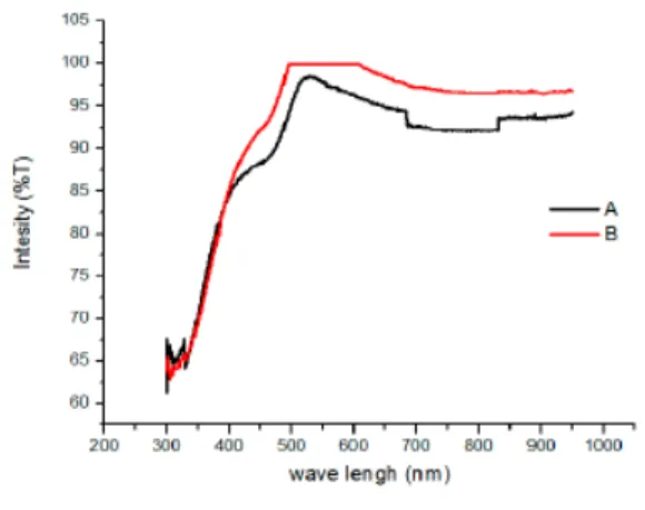
(4) https://cimav.repositorioinstitucional.mx/ the same conditions as above, so some changes were made as increasing and decreasing concentration of thiourea as it is responsible for carrying out the reaction, also tried to play with the pH changing it 11-9. A review of the washing procedure and substrate preparation was necessary in addition to increasing the time growth. These substances were placed in a water bath at 70 ° C, and continued with same conditions but still did not made the deposit check. But we know where the change. Optical Transmission Measurements Optics UV-Vis characterization It took the most representative films for this article. Figure 1 shows UV-visible curves, where A represents the film without adjustment of temperature and B with adjustment of the temperature. We can appreciate a dominant shoulder placed at 527 nm, which is consistent with that reported in the literature [5] and a transparent region up to 1000 nm., Samples analyzed with Origin Software 6 [12]. 4.
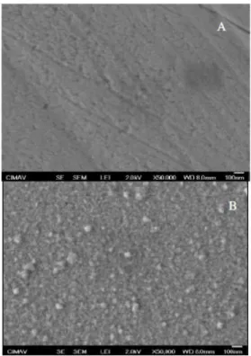
(5) https://cimav.repositorioinstitucional.mx/ Moreover, in a Figure 2 shows the curve of the band gap, here we observe that the energy of the gap is 2.54 eV which is in excellent agreement with that reported in the literature. [13, 14].. Characterization by Scanning Electron Microscope (SEM) The micrographs were analyzed in a microscope that uses an electron beam, which has a resolution of 2 nm, was operated at a voltage of 8.0 kV in the secondary electron mode, with amplifications from 50000X, and working distance of 8mm. Figure 3 presents the SEM characterization representations. In Figure 3 A is clear the presence of a flat film and the film B shows an irregular surface may be due to agglomeration of the deposition, which were confirmed by AFM characterization in section D.. 5.
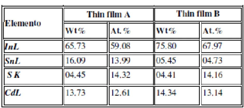
(6) https://cimav.repositorioinstitucional.mx/. Characterization of Energy Dispersive Spectroscopy (EDS): Figure 4 presents the EDS analysis, where we can observe that the ratio of Cd and S have a slight increase in B with respect to A.. 6.
(7) https://cimav.repositorioinstitucional.mx/ Table 1 shows the relationship between film and the concentration of the elements.. Morphological Representation AFM With a general view of 5×5μm and 1x1μm amplification. Figure 5 expresses the behavior of the material in which A has no agglomeration is more homogeneous growth whereas in a film B is presented in the form of an agglomeration islets with VolmerWeber type growth. On the other side, Figure 6 presents the 3D representation of the nanostructured CdS surface.. 7.
(8) https://cimav.repositorioinstitucional.mx/. During the deposition of materials on substrates, the agglomerate is caused by the interaction between the deposited materials underlying substrate, even under thermodynamic equilibrium. There are three types of growth: two-dimensional (2D) layer (Frank-van der Merve, FM) mode, three-dimensional (3D) island (Volmer-Weber, VW) mode 2D and 3D layer followed by island (Stranski -Krastanov, SK).. 8.
(9) https://cimav.repositorioinstitucional.mx/. In the VW and SK growth, [15, 16] the agglomeration inevitably appears in thermodynamic equilibrium conditions. In the case of this research have shown growth VW in the film B, which is favored in case the binding energy between the atoms deposited Promotions Specialties the binding energy of the atoms of the substrate. , In Figure 7 are expressed growth rates. [17, 18].. 9.
(10) https://cimav.repositorioinstitucional.mx/. By identifying the type of growth took the grain size of the agglomerates with the software WSxM SPM [11, 18, 19] as shown in Figure 8 with the extension of the film.. 10.
(11) https://cimav.repositorioinstitucional.mx/. With these data we proceeded to graph a power 350 grain lengths at intervals of every 20 as a mark of class as shown in Figure 9. Conclusions The experiments were performed at room temperature, therefore it had to match this temperature our substances, for the reaction happen at the same initial conditions, so it is concluded that what was the temperature concerned. The following steps were performed as mentioned in the experimental section. Replicas which were conducted by adjusting the temperature resulted in an agglomeration formed under limited or kinetically thermodynamic equilibrium conditions at constant temperature. Through the use of microscopy, we studied the dynamics of growth and formation of CdS thin films on glass / ITO, where three-dimensional growth was observed through agglomerated grain, following the Volmer-Weber model. The evolution of the average. 11.
(12) https://cimav.repositorioinstitucional.mx/ grain diameter is of the order of 200nm, concluding that the more the grain size is greater the efficiency of the film, while the average thickness of 112.96 nm. References [1] Zapata-Torres, M., Peña, J. L., & Calzadilla-Amalla, O. (2003). Caracterizacion por difraccion de rayos-X de peliculas delgadas de CdSx T1-x. Sociedad Mexicana de Ciencia de Superficies y de Vacío, 40-44. [2] Aramoto, T., Kumazawa, S., Huguchi, H., Arita, T., Shibutani, S., Nakajima, J., y otros. (1997). Jpn. J. Appl. Phys., 36. [3] Romero, N., Bvossio, A., Tedishi, R., & Canevari, V. (1998). Dnd. World Conference and Exhibition on photovoltaic solar energy convension. Viena Austria. [4] Oliva, A. I., Solis-Cano, O., Catro-Rodriguez, R., Sosa, V., & Quintana, P. (2000). Peliculas delgadas de CdS: Preparacion y comparacion de propiedades usando diferentes tecnicas de deposito. Sociedad Mexicana de Ciencia de Superficie y Vacio, 15-19. [5] Flores limas, J. A., Peña, J. L., Martinez Guerra, E., & PerezTijerina, E. (2011). Primeras Etapas en el crecimiento de peliculas delgadas de teleuro de cadmio (CdTe). Redalyc Sistema de Informacion Cientifica, 46-52. [6] Duran-Arjona, M. (2007). Efecto de dos metodos de deposito de CdS y la eficienia de celdas solares CdS/CdTe. [7] Hodes, G. (2003). Chemical Solution Deposition of Semiconductor Films. New York. Basel.. 12.
(13) https://cimav.repositorioinstitucional.mx/ [8] Chang, Y., Munsee, C. L., Herman, G. S., Wager, P., Mugdur, P., Lee, D. H., y otros. (2005). Growth, characterization and application of CdS thin films deposited by chemical bath deposition. Surface and Interface Analiysis, 398-405. [9] Ochoa-Landin, R., Sastre-Hernandez, J., Virgil-Galan, O., & RamirezBon, R. (2010). Chemically deposited CdS by an ammonia-free process for solar cell windows layers. Solar Energy. [10] Mazón, D., & Sotelo, M. (s.f.). Estudio del Mecanismo de Crecimiento de Peliculas Delgadas de Sulfuro de Cadmio (CdS) depositadas por Baño Químico. [11]. (s.f.). WSxM SPM SOFTWARE. Obtenido de http://www.nanotec.es/products/wsxm/ [12] Candal, R. J., Bilmes, S. A., & Blesa, M. A. (s.f.). Semiconductores con Actividad Fotocataliticas. [13] Memming, R. (1988). Photoelectrochemical Solar Energy Conversion. Topics in Current Chemistry, 143. [14] MacDonald, J. (1975). Surface Physics of Materials. [15] Venegas, A., Edison, J., Flores, D., & Garzón, S. (2012). Sputtering, Peliculas Delgadas y crecimiento Epitaxial. [16] Devia-Cubillos, A. (2003). Produccion y caracterización de Recubrimientos en Multicapas de TiN/DLC en Peliculas Delgadas. [17] Quiñones, J. G. (2008). Síntesis y caracterización de películas delgadas de la aleacion Si!-x-yGexCy depositadas mediante ablacion. 13.
(14) https://cimav.repositorioinstitucional.mx/ laser. 19. [18] Microcal-Sofware, I. (s.f.). Originin 6. [19] Gómez-Rodriguez, J. M., Colchero, J., Gómez-Herrero, J., & Baro, A. M. (2007). Review of Scientific Instrument.. 14.
(15)
Figure
Documento similar