Photoluminescence Imaging and LBIC Characterization of Defects in mc-Si Solar Cells
1
2
L.A. Sánchez1,2, A. Moretón1, M. Guada1, S. Rodríguez-Conde1, O. Martínez1, M.A. González1 and J.
3
Jiménez1,
4
1.—GdS-Optronlab, Dpto. Física de la Materia Condensada, Universidad de Valladolid, Edificio LUCIA,
5
Paseo de Belén 19, 47011 Valladolid, Spain. 2.—e-mail: [email protected]
6
7
ABSTRACT
8
Nowadays the photovoltaic market is dominated by multicrystalline silicon (mc-Si) based solar cells with
9
around 70% of worldwide production. In order to improve the quality of the Si material, a proper
10
characterization of the electrical activity in mc-Si solar cells is essential. A full-wafer characterization
11
technique like photoluminescence imaging (PLi) provides a fast inspection of the wafer defects at the
12
expense of the spatial resolution. On the other hand, a study of the defects at a microscopic scale can be
13
achieved through the light-beam induced current (LBIC) technique. The combination of these macroscopic
14
and microscopic resolution techniques allows a detailed study of the electrical activity of defects in mc-Si
15
solar cells. In this work, upgrade metallurgical-grade (UMG) Si solar cells are studied using these two
16
techniques.
17
18
KEY WORDS: solar cells, multicrystalline silicon, UMG silicon, LBIC, photoluminescence
1
INTRODUCTION20
Multicrystalline silicon (mc-Si) is currently the basis of the photovoltaic (PV) market due to its low
21
production cost and relatively high efficiency. Upgraded metallurgical-grade silicon (UMG Si) has raised
22
as an alternative to the traditional purification obtained by Siemens process because of the reduced
23
production cost and time [1, 2]. Although the Siemens process produces the purest material, solar cells
24
fabricated with wafers from UMG Si have achieved efficiencies around 20% [3].
25
UMG Si contains more impurities, like shallow acceptors and donors, which reduce the carrier diffusion
26
lengths and limit the cell efficiency [4]. In order to improve the quality of the UMG Si, it is essential to
27
know the type of defects and the detrimental role played by the trapping centers for the photogenerated
28
carriers. Photoluminescence imaging (PLi) and light-beam induced current (LBIC) techniques have
29
demonstrated to be powerful characterization tools for measuring the electrical activity of defects in mc-Si
30
solar cells [5-8]. In PLi, the surface of the sample is excited with optical radiation to emit luminescence and
31
a CCD camera is used to acquire the luminescence emission signal. This technique does not require
32
electrical contacts and is applicable not only to solar cells, but also to bricks, as-cut wafers and processed
33
wafers [9]. PLi provides a macroscopic spatially-resolved image of the electrical activity of a solar cell in
34
a short time (seconds), depending on the quantum efficiency of the camera. Silicon CCD cameras can detect
35
only a very small portion of the Si band to band luminescence emission, usually it requires long exposure
36
times. However, InGaAs cameras are sensitive to the luminescence spectrum of Si, and operate at shorter
37
exposure times than the Si CCD cameras. Dark contrasted areas in the images obtained by PLi can be
38
associated with grain boundaries, dislocations, micro-cracks, etc. In LBIC, a laser beam is focused and
39
scanned point by point over a surface area of the solar cell, and the generated electron-hole pairs produce a
40
photocurrent [10]. This photocurrent is collected at each point of the selected area and its intensity is
41
governed by the trapping of minority carriers. LBIC images reveal the spatial distribution of the trapping
42
centers. This technique, instead of PLi, allows a very high spatial resolution, but it is time consuming as
43
compared to PLi. In this work we study defects in UMG mc-Si solar cells at macroscopic and microscopic
44
scales using these two techniques.
45
46
EXPERIMENTAL
47
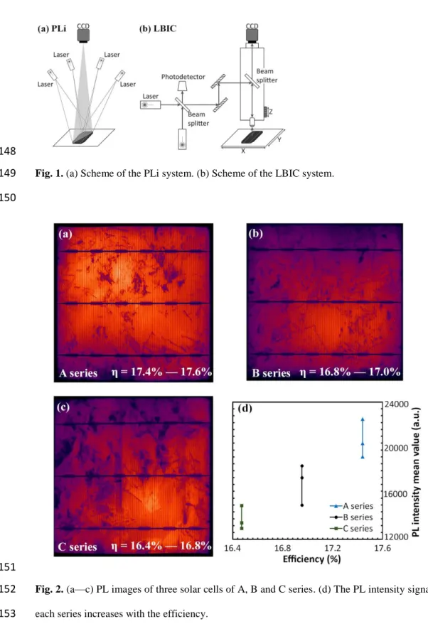
PL imaging was measured by the homemade setup represented schematically in Fig. 1a. The PLi excitation
48
system contains four 20 W laser diodes (808 nm wavelength). The photoluminescence emission of the solar
2
cell is captured in a dark environment with a 1392x1040 pixels Si-CCD camera (PCO 1300 solar). In order
50
to get a full image of the solar cell a 12.5 mm focal length objective is coupled to the camera. A longpass
51
filter with a cutoff wavelength of 900 nm was mounted in front of the camera to remove the background
52
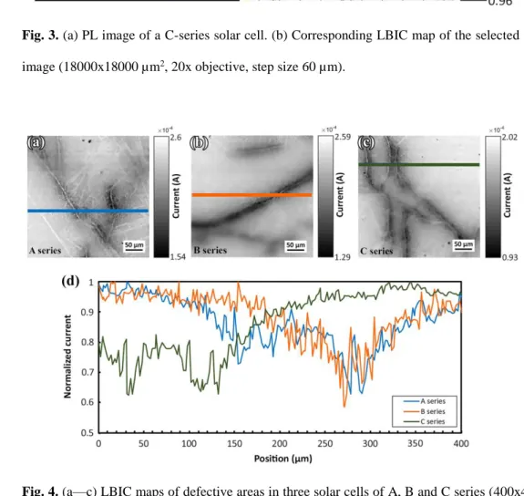
light. PL emission was also captured with an InGaAs camera (Hamamatsu C12741-03).
53
A homemade LBIC system was used to obtain higher detailed information about the defects in the solar
54
cells. The scheme of the LBIC setup is shown in Fig. 1b. The LBIC apparatus consists of four excitations
55
wavelengths from two dual laser diodes (Omicron). The laser lines are 639, 830, 853 and 975 nm, and they
56
allow to achieve different penetrations depths. In the studies presented here only the 853 nm line was used.
57
A beam-splitter divides the output beam of the laser (10 mW) into two beams. One of them is used to
58
measure variations in the output power through a photodiode. The other one is directed into a trinocular
59
microscope which focuses the laser onto the solar cell. Different objectives (20x, 50x, 100x) enable studies
60
up to a very high spatial resolution, circa 1 m for the 100x objective. A Si-CCD camera coupled to the top
61
ocular is used to collect the light reflected by the sample and drive the auto-focus system through edge
62
detection. The LBIC scanning is obtained by moving the sample in an x-y-z motorized translation stage
63
(Prior Scientific) over areas as large as 76.7 x 114.5 mm2 and step sizes as small as 1 µm. The photocurrent
64
generated is collected by an electrometer (Keithley Instruments) and data acquisition and hardware control
65
was developed in LabVIEW.
66
UMG mc-Si solar cells provided by Silicio Ferrosolar were characterized through the PLi and LBIC
67
techniques. The measures were carried out on three series of UMG mc-Si solar cells. A-series have
68
efficiencies ranging between 17.4 and 17.6%, B-series have efficiencies between 16.8 and 17.0% and
C-69
series have efficiencies between 16.4 and 16.8%.
70
71
RESULTS AND DISCUSSION
72
Figs. 2a—c show the PL images obtained in three solar cells corresponding respectively to series A, B and
73
C. These images presented dark areas that mainly correspond to grain boundaries and intragrain defects. A
74
first look to these images shows that the C-series solar cell image contains a greater number of dark areas.
75
The three series of measured solar cells yielded different values of photoluminescence intensity signal.
76
Higher values of efficiency produced higher values of the intensity of the PL emission of the solar cell.
77
This PL intensity signal is expressed through the mean value of the intensity over all the pixels of the PLi
78
image. An almost linear dependence is shown in Fig. 2d, where the maximum, minimum and mean value
3
of this PL intensity signal is plotted for each solar cell series. Very similar results were found with the two
80
cameras used in the experiment, the Si CCD camera and the InGaAs camera. In the second one, the exposure
81
times used are lower because of the higher quantum efficiency of the InGaAs sensor around the wavelength
82
at which silicon emits.In particular, the exposure time values used in the experiments are 150 ms for the
83
InGaAs camera against 30 seconds for the Silicon CCD.
84
Fig. 3 shows the PL image of a C-series solar cell as well as the LBIC map of a highly defective zone
85
obtained with a 20x objective. Whereas the PLi measurement showed an almost uniform dark zone because
86
of the poor spatial resolution, the LBIC map allowed to appreciate the structure of the defects, which
87
appears as an array of dark contrasted lines, thanks to the greater spatial resolution obtained with this
88
technique. The LBIC contrast is higher due to the large photocurrent generated by the laser beam over a
89
small area. The LBIC measure took about 24 hours to map this 18000x18000 µm2 region of the solar cell
90
with a lateral resolution of 60 µm. More detailed information about these defects can be obtained by using
91
a high magnification objective. Figs. 4a—c show 400x400 µm2 LBIC maps of A, B and C-series solar cells
92
using a 100x objective. These measurements revealed a slightly bright contrasted line along the core of the
93
defects in all the series. This local bright contrast is probably due to a depletion of impurities. The impurities
94
tend to accumulate at both sides of this bright line resulting in dark regions of high trapping activity. Fig.
95
4d shows the normalized photocurrent profiles across the lines marked in Fig. 4a—c. The ratio between
96
currents generated in non-defective and defective areas is essentially the same on the three solar cells, so
97
the lower efficiencies in B and C series can be explained not as an increase of the electrical activity of the
98
defects but as the consequence of a greater density of defects.
99
Some of the B and C-series solar cells presented micrometric size dark spots around the defects in some
100
regions (Fig. 5a), with a pronounced drop in the photocurrent. Fig. 5b shows the reflected light map of a
C-101
series sample obtained with the Si-CCD camera coupled to the microscope. This map revealed information
102
about the higher photocurrent generated at the core of the defects as a consequence of a lower reflectivity,
103
but no information is obtained about these dark spots. UMG Si contains more metallic impurities than
104
traditional solar grade Si, so these dark spots can be explained as an accumulation of metallic impurities
105
which give rise to clusters with high electrical activity [11]. The reflected map also showed low reflective
106
regions without high capture rates around them in the corresponding LBIC measurement. The goal of future
107
studies will be an accurate measurement of the total light power reflected by the cell in order to provide a
4
tool to calculate the internal quantum efficiency (IQE) and effective diffusion length (Leff) of the minority
109
carriers, using the different excitation wavelengths integrated in the LBIC system.
110
efficiencies through PLi and LBIC techniques. PLi allowed a fast full-wafer observation of the cells, with
114
a good correlation between the mean value of PL intensity signal and the solar cell efficiencies. A detailed
115
description of the defective areas revealed by PLi was achieved by high spatial resolution LBIC mapping.
116
The photocurrent ratio between non-defective and defective areas was the same for the three series of cells.
117
Solar cells with lower efficiencies presented dark spots around some of the defects. Reflected light mapping
118
allowed to establish a correlation between LBIC maps and surface features but no information about these
119
dark spots was revealed.
120
121
ACKNOWLEDGEMENTS
122
This work was supported by the Spanish MINECO project, ref. ENE2014-56069-C4-4-R and “Junta de
123
Castilla y León (Spain)” project number VA081U16. We thank Silicio Ferrosolar for providing the samples
124
studied in this work.
125
Aratani, Prog. Photovolt: Res. Appl. 9, 203–209 (2001).
129
[2] D. Kohler, B. Raabe, S. Braun, S. Seren and G. Hahn, in Proceedings of the 24th European Photovoltaic
130
Solar Energy Conference (2009), pp. 1758–1761.
131
[3] F. Rougieux, C. Samundsett, K. C. Fong, A. Fell, P. Zheng, D. Macdonald, J. Degoulange, R. Einhaus,
132
and M. Forster, Prog. Photovolt: Res. Appl. 24, 725–734 (2016).
133
[4] M. Forster, P. Wagner, J. Degoulange, R. Einhaus, G. Galbiati, F. Rougieux, A. Cuevas and E.
134
Fourmond, Sol. Energy Mater Sol. Cells 120, 390–395 (2014).
135
[5] T. Trupke, B. Mitchell, J. W. Weber, W. McMillan, R. A. Bardos and R. Kroeze, Energy Procedia 15,
136
135-146 (2012).
137
[6] M. Bliss, X. Wu, K. Bedrich, T. Betts and R. Gottschalg, IET Ren. Pow. Gener. 9, 446–452 (2014).
5
[7] B. Moralejo, M. A. González, J. Jiménez, V. Parra, O. Martínez, J. Gutiérrez and O. Charro, J. Electron.
139
Mater. 39, 663–670 (2010).
140
[8] M.K. Juhl, M.D. Abbot, T. Trupke, IEEE J. Photovolt. 7, no. 4, 1074–1080 (2017).
141
[9] B. Moralejo, A. Tejero, O. Martínez, M. A. González, J. Jiménez and V. Parra, in Proceedings of the
142
2013 Spanish Conference on Electron Devices (2013), pp. 353–356.
143
[10] B. Moralejo, V. Hortelano, M. A. González, O. Martínez, J. Jiménez, S. Ponce-Alcántara and V. Parra,
144
Phys. Status Solidi (c) 8, 1330–1333 (2011).
145
[11] J. Chen, B. Chen, W. Lee, M. Fukuzawa, M. Yamada and T. Sekiguchi, Solid State Phenomena 156–
146
158, 19–26 (2010).
6
148
Fig. 1. (a) Scheme of the PLi system. (b) Scheme of the LBIC system.
149
150
151
Fig. 2. (a—c)PL images of three solar cells of A, B and C series. (d) The PL intensity signal obtained for
152
each series increases with the efficiency.
153
7
155
Fig. 3. (a) PL image of a C-series solar cell. (b) Corresponding LBIC map of the selected area in the PL
156
image (18000x18000 µm2, 20x objective, step size 60 µm).
157
158
159
Fig. 4. (a—c) LBIC maps of defective areas in three solar cells of A, B and C series (400x400 µm2, 100x
160
objective, step size 2 µm). (d) Normalized photocurrent profiles across the lines marked in Fig. 4a—c.
161
8
163
Fig. 5. (a) LBIC map of a C-series solar cell area presenting dark spots (400x400 µm2, 100x objective, step
164
size 2 µm). (b) Corresponding reflected light map. Some of the low reflective regions have a high electrical
165
activity in the LBIC map, while others do not.