asymmetric filters make use of a binomial impedance transformer in each filter section. The asymmetric filters (one low pass filter, LPF, and other high pass filter, HPF) allow the balun bandwidth to be increased while the binomial transformer matches the variable balanced dipole impedance. In this way the ripple in the balun response due to the variation of the UWB dipole impedance is reduced. A balun for a UHF and UWB dipole antenna working from 220 to 820 MHz (bandwidth of 4:1) has been achieved with losses lower than 1 dB. These types of baluns are particularly useful in the low microwave frequency band.
Index Terms—Baluns, UHF antennas, ultrawideband (UWB) antennas.
I. INTRODUCTION
Microwave baluns provide balanced outputs from an unbalanced input. Baluns in dipole antennas deliver half the input amplitude signal towards both output terminals out of phase by 180 with respect to each other. Microwave baluns can be realized in either distributed or lumped-element technology.
In the early literature one of the most popular baluns made with dis-tributed technology was due to Marchand [1]. Its non-planar geom-etry and large size made it unsuitable for printed circuit processes. One printed version of the Marchand balun can be found in [2]. However, this still requires several printed layers that also implies a large size, especially in the low microwave frequency band. Baluns made with lumped element technology overcome the size problem presenting a more compact aspect. This last fact results in them playing an impor-tant role in the design of low frequency planar antennas.
Among lumped circuit baluns, the simplest is the so called lattice-balun structure [3]. In this configuration, the 3 dB cutoff frequency in any of the filter sections is the centre of the balun bandwidth. In addi-tion, a phase difference of 180 between the balun outputs is naturally obtained. Finally, the balun bandwidth can be enlarged by increasing the order of the two filters at a price of raising both the ripple band-width and the losses.
Recently, in [4], a second order lattice-balun based on lumped el-ement technology has been proposed to get broadband performance. Each filter (LPF and HPF) in the lattice structure consists of a T-filter section. The shunted T-section equalizes the phase difference over the common bandwidth of the two filters. This broadband lattice balun is a
Manuscript received March 21, 2007; revised October 21, 2007. Published July 7, 2008 (projected). This work was supported in part by the Spanish MEC under Project TEC2006-13248-C04-04/TCM.
V. González-Posadas and J. L. Jiménez-Martín are with the Department of Ingeniería Audiovisual y Comunicaiones, UPM, 28031 Madrid, Spain (e-mail: [email protected]).
C. Martín-Pascual is with the Department of Signal Theory and Communica-tions, Carlos III University in Madrid, 28911 Leganés, Madrid, Spain.
D. Segovia-Vargas is with the Department of Signal Theory and Communica-tions, Carlos III University in Madrid, 28911 Leganés, Madrid, Spain (e-mail: [email protected]).
Color versions of one or more of the figures in this paper are available online at http://ieeexplore.ieee.org.
Digital Object Identifier 10.1109/TAP.2008.924769
antenna impedance into the one desired. An analysis of the output phase-balanced parameter versus the filter order is also undertaken to show the balun performance. Section III provides a practical example with a lumped element balun connected to an UWB dipole in the UHF band. Finally Section IV presents the conclusions.
II. BALUNDESIGN
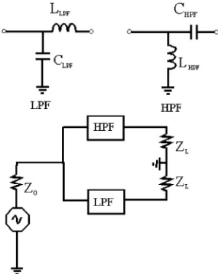
The balun is intended to be connected to an UWB UHF dipole an-tenna. The antenna input impedance shows a large variation (a typical value for the ratio between the highest and lowest impedance is 3:1). The lumped element technology has been chosen in designing the pro-posed compact balun. This balun consists of two branches, one with an LPF and the other with an HPF. The filters’ cutoff frequencies have been shifted from the central balun frequency to achieve the desired bandwidth. Each filter, LPF and HPF, is designed by the cascading of elementary L-sections as shown in Fig. 1. The number of sections has been chosen to reduce the ripple as much as possible, while keeping the desired frequency bandwidth. In this way the design procedure aims for a balance transmission (both in amplitude and phase) from an unbal-anced port to a balunbal-anced dipole presenting a large impedance margin through a broad bandwidth. Thus, the design procedure can be summa-rized as follows.
• Choice of the type of lumped element filter and selection of the cutoff frequencies in the HPF and LPF to get a broadband balun. • Design of the impedance transformers to achieve a balun for
vari-able balanced impedances.
• Selection of the number of sections at the transformer to reduce the ripple in the desired bandwidth.
Firstly, the lumped elements HPF and LPF are designed to have a phase difference of 180 between balanced outputs in a broad bandwidth. By mixing LPF (supporting forward waves) and HPF (supporting backward waves) a phase difference of 180 between terminals 2 and 3 can be achieved. For simplicity, and without loss of generality, this analysis can be undertaken for the single section L-network shown in Fig. 1. In this case it can be seen that if the input voltage were V, the terminal voltages would be given by
(1)
where is the voltage at the th port and and are poly-nomials of the frequency variable. If the ratio between the outputs at nodes 2 and 3 is extracted for the single section filter case it results in
(2)
where , are the inductors and capacitors for the LPF while , are the corresponding values for the HPF.
It can be seen that ports 2 and 3 are 180 out of phase. Therefore, the balanced performance requires that the path between the second
Fig. 1. Block diagram and schematic of the proposed balun.
and third nodes have an equal number of LPF and HPF sections. In this case, in order to deal with the variable output balanced impedance, the values for the lumped elements do not follow a symmetric arrangement. For that reason, the lattice network is discarded and an arrangement of LPF between ports 1 and 2 is chosen. In the same way, an arrangement of HPF between ports 1 and 3 is selected. It must be emphasized that in these arrangements the number of LPF and HPF sections has to be the same to keep an out of phase performance of 180 between 2 and 3 ports.
The next step is the design of the elementary “L” networks for each of the transmission line segments. These filters do not have the same cutoff frequencies since the overall broadband balun performance needs two frequency shifts: towards higher frequencies in the LPF and towards lower frequencies in the HPF. Then, the lumped elements (L and C) in the LPF are given by
(3)
where is the impedance of the corresponding transmission line section and is the upper cutoff frequency of the LPF. The lumped elements for the HPF are
(4)
where is the admittance of the corresponding transmission line section and is the lower cutoff frequency of the HPF. Both and are not equal and are obtained by shifting the cen-tral frequency a magnitude resulting in
(5)
The impedance transformation ratio between the unbalanced and balanced ports is simply determined by the filters’ characteristic im-pedances as
(6)
where is the unbalanced load impedance (real or apparent at any section of multi-section transformer) and is the unbalanced source impedance.
Fig. 2. Diagram of the characteristic impedances in the multisection transformer.
The second step in the design process deals with the broadband dipole variable impedance. Actually, the load impedance margin in a broadband antenna usually keeps a ratio larger than 3:1. For that reason the uniform multi-section transformer is discarded while the binomial or Chebyshev types are considered. For the lumped element balun design, it has been seen that there are no great differences between both transformers. As the transmission response must be as flat as possible for the overall impedance margin, the binomial transformer has been chosen. For the binomial case, the total reflection coefficient
is given by
(7)
where is the number of sections and is the electrical length of the corresponding section in the transformer. For the binomial transformer this yields
(8)
where are the binomial coefficients. This leads to the first-order re-flection coefficients (defined as the rere-flection coefficient between two adjacent sections in the binomial transformer). Therefore, the transmis-sion line characteristic impedances at the multisection transformer are set in a geometrical progression. Equation (9) shows the transforming expressions for the -section filter
(9)
In the previous expressions the first subindex denotes the order of the implemented filter while the second subindex denotes the th section of the corresponding -section filter. The process to get the values is obtained according to (9). This process is illustrated in Fig. 2. The left part of the figure indicates the input unbalanced impedance while the right part designates the output balanced dipole impedance . The central part shows the impedances for each filter section. The row number, associated with a fixed th subindex, denotes the order of the corresponding HPF or LPF. The vertical arrows suggest the way to obtain any L-section impedance. In this way, for a fixed order filter the values of its section impedance
are obtained from the values in the previous rows by following the recursive calculus as shown in (9).
Fig. 3. Broadband dipole for UHF applications.
Finally, the order of the filter has to be considered. It is well known that as the number of sections increases, the bandwidth can be enlarged. In spite of this, as the balun performance is determined by a frequency shift in both the LPF and the HPF, the filter behavior at the cutoff re-gions must be considered. It has been seen that due to the Gibbs phe-nomenon, as the number of sections increases the ripple at the cutoff regions of the desired bandwidths is more critical. As the balance set-ting at ports 2–3 (outputs from the LPF and HPF) is critical, this ripple affects the overall balun response. For that reason, the number of sec-tions can not be large and a tradeoff between the number of secsec-tions and the allowed ripple has to be made.
III. RESULTS ANDDISCUSSION
The antenna proposed for this application is a planar dipole with a large impedance bandwidth. Each of the arms of the dipole is a trun-cated irregular rhombus as can be seen in Fig. 3.
The antenna design parameters are the length of the arm (292 mm), the width of the arm (97 mm) and width of the truncated arm (18 mm). These parameters have been optimized to achieve the proposed impedance bandwidth, from 200 to 800 MHz.
The first step in the design procedure is to measure the dipole impedance to find the impedance variation margin. Fig. 4 shows the measured balanced dipole impedance without the balun in a band from 200–800 MHz. From that figure it can be seen that the mean value of the balanced antenna impedance is around 150 ohm
.
Thus, the maximum value for the unbalanced impedance, , is around 75 ohm . For that reason, that is the starting value in designing the multisection binomial transformer. From (9), Fig. 4 and following the impedance notation in Fig. 2, Table I can be extracted. Each column in Table I corresponds to the th section. Each row corresponds to the implementation of the th order filter. The last column corresponds to the value of the unbalanced impedance.
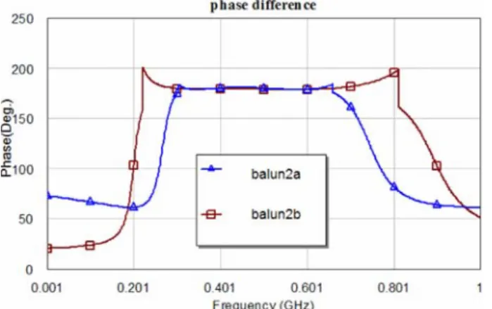
By shifting the frequency of the LPF (towards ) and the HPF (towards ), an increase in the bandwidth of the balanced re-sponse is achieved. Several prototypes have been built according to the parameter. The ratio has been taken as 0.33 and 0.5. Fig. 5 shows the amplitude response for the 2nd order filter balun with a filter ratio of 0.33 and 0.5 (henceforth balun2a will refer to a balun with a filter with two sections and a filter ratio of 0.33 while balun2b will refer to a balun with a filter with two sections and a filter ratio of 0.5). It can be seen that the ripple is somewhat similar for both de-signs. However, concerning the frequency bandwidth, it can be seen that the balun with a filter ratio of 0.5 presents a larger bandwidth, up to 2 octaves.
The phase performance for each of the two filter ratios is shown in Fig. 6. It can be seen that a relative flat phase difference of 180 has
Fig. 4. Broadband dipole antenna impedance without the balun.
Fig. 5. Amplitude response of the 2nd order balun for a filter ratio of 0.5 (balun2b) and 0.33 (balun2a).
TABLE I
IMPEDANCEVALUESVERSUS THENETWORKORDER
been obtained for a bandwidth ratio of nearly 4:1 (for the 0.5 filter ratio) and nearly 3:1 (for the 0.33 filter ratio).
Fig. 6. Phase difference between ports 2 and 3 of the 2nd order balun for a filter ratio of 0.33 (balun2a) and 0.5 (balun2b).
Fig. 7. Amplitude response of LPF (continuous) and HPF (dotted). The filter order is 1st, 2nd, and 6th.
the transmission response and the phase error increases dramatically, especially at the bandwidth cutoff region. This limits the structure to a second order balun.
Finally, an additional transmission line has been added at the output balanced ports (2 and 3) to compensate a slight shifting in the phase difference and achieve a phase difference of 180 . Fig. 9 shows the constructed balun with 0603 SMD components at a central frequency of 450 MHz. According to Table I, each filter section characteristic impedance is 55.2 and 67.8 ohm, respectively. In the L-type LPF arm the values of the inductors and capacitors are 15 nH, 18 nH, 4.7 pF, and 3.9 pF, respectively. In the L-type HPF arm, the values are 30 nH, 36 nH, 10 pF, and 8.2 pF.
Figs. 10–12 show the simulated and measured reflection and trans-mission coefficients (this last one, in amplitude and phase) at the input and output ports. Good agreement has been achieved for the three pa-rameters between measurements and simulations. Measurements also show that a 0.5 filter ratio achieves a 4:1 bandwidth. The insertion losses in both the HPF and the LPF are lower than 1 dB (with a ripple of ) from 220 to 800 MHz.
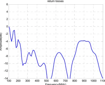
Lastly, the performance of the balun connected to the antenna is shown in Figs. 13–15. The reflection coefficient of the antenna con-nected to the balun shows the return losses are lower than 7 dB through a bandwidth from 220 MHz up to 820 MHz.
The difference in the amplitude response between the two dipole arms is shown in Fig. 14. A maximum difference of 2.2 dB has been
Fig. 8. Phase response of LPF (continuous) and HPF (dotted). The filter order is 1st, 2nd, and 6th.
Fig. 9. Balun prototype based on 2nd order filters.
Fig. 10. Simulated (dotted) and measured (continuous) input reflection coeffi-cient for the 2nd order balun for a 0.5 filter ratio.
Fig. 11. Simulated (dotted) and measured (continuous) transmission parame-ters - for the 2nd order balun for a 0.5 filter ratio.
Fig. 12. Simulated (dotted) and measured (continuous) phase difference for the 2nd order balun for a 0.5 filter ratio.
Fig. 13. Return losses at the input of the balun connected to the broadband dipole antenna.
Fig. 14. Difference in the amplitude response at the input of the two dipole arms.
Fig. 15. Phase difference at the input of the two dipole arms. The dashed line represents a 170 phase difference.
This error can be associated with the parasitic effects of the lumped elements and the fact that the inductances and capacitances are not ex-actly equal to the designed values. A statistical analysis has been un-dertaken to see the effects of the parasitic effects and lumped element tolerances on the overall balun performance. The study mainly pays attention to the balun insertion losses, return losses and phase differ-ence responses. The parameters analyzed are: capacitors, inductors and substrate permittivity. In a first stage the values of these parameters are modified independently from each other element over their whole tolerance margin. In a second stage a tolerance study on the simulta-neous variation of the capacitors, inductors and substrate permittivity has been done. The simulation analysis has been done with AWR. The number of analysis for any of the two stages has been set to 5000. The parameter tolerance has been set to 10% for all the components values, following the maximum value in the data sheet.
Fig. 16. Variation of the simulated amplitude response versus the inductance. The dark trace corresponds to the measurement.
Fig. 17. Variation of the simulated amplitude response versus a jointly variation of the tolerance parameters. The dark trace corresponds to the measurement.
which are more sensitive and are somewhat out of this margin. It has also been seen that the least critical parameter is the permittivity since its variation affects the balun performance slightly. The most critical parameter is the inductor while the capacitor variation shows some termediate performance between the one of the permittivity and the in-ductor parameters. As an example, Fig. 16 shows the amplitude balun performance versus the independently variation of the inductance.
From the second analysis stage it can be concluded that the balun performance suffers from larger variation than in the previous case since all the tolerance parameters are changing at the same time. As an example, Fig. 17 shows the amplitude balun performance versus the jointly variation of the capacitance, inductance and permittivity. Nonetheless, the balun still presents a good amplitude and phase bal-ance performbal-ance through an approximate 4:1 bandwidth.
IV. CONCLUSION
A semi-lumped balun transformer for UHF and UWB dipoles has been presented in this paper. The proposed structure is based on two asymmetric 2nd order filters: one low pass filter and one high pass filter. The UWB performance has been achieved by shifting the HPF cutoff frequency toward lower frequencies and the LPF cutoff frequency to-ward higher ones. In addition, these filters also transform the variable antenna impedance into the desired source impedance by making use of a binomial transformer. Good agreement between simulations and measurements has been achieved. The prototype circuit shows good amplitude balance with a phase difference of 180 across a 4:1 band-width from 220–820 MHz. The losses are lower than 1 dB along the whole bandwidth.
[3] W. Bakalski, W. Simbürger, H. Knapp, H. Wohlmuth, and A. L. Scholth, “Lumped and distributed lattice-type LC-baluns,” inIEEE MTT-S Int. Microwave Symp. Digest, 2002, pp. 209–212.
[4] D. Kuylenstierna and P. Linner, “Broadband lumped element baluns with inherent impedance transformation,”IEEE Trans. Microw. Theory Tech., vol. 52, pp. 2739–2745, Dec. 2004.
[5] S. J. Parisi, “180-degree lumped-element hybrid,” inIEEE MTT-S Di-gest, 1989, pp. 1243–1246.
[6] R. E. Collin, Foundations for Microwave Engineering. New York: McGraw-Hill, 1992.
Design of Ultrawideband Mobile Phone Stubby Antenna (824 MHz-6 GHz)
Zhijun Zhang, Jean-Christophe Langer, Kevin Li, and Magdy F. Iskander
Abstract—An ultrawideband stubby antenna that covers all frequency bands between 824 MHz and 6 GHz, which include GSM 850 and 900, GPS, DVB-H US, DCS, PCS, UMTS, BT, WLAN 802.11b/g and WLAN 802.11a, with a VSWR better than 2.7:1 is described in this paper. The design pro-cedure involves obtaining a wideband resonance from 1–6 GHz and using a matching network to compensate for the high capacitance of the antenna at the lower frequency band below 1 GHz. Parametric studies of this antenna are presented in this paper. The design was experimentally verified by con-structing an ultrawideband antenna with a volume of . It is significant that the designed ultrawideband stubby antenna maintained a good impedance matching and radiation efficiency at all bands. An ef-ficiency between is achieved in the lower band including band required for the GSM 850 and GSM 900 sys-tems, and an efficiency value of is achieved at the rest of the bands starting with the GPS at 1575 MHz to 6 GHz.
Index Terms—Matching network, monopole antennas, multiband
antennas, wideband antennas.
I. INTRODUCTION
With the rapid growth of mobile communication industry, more and more functionalities are being integrated into a single mobile device. Meanwhile, the overall device size and also the available space inside a device for antennas are consistently shrinking. Five
Manuscript received July 23, 2007; revised January 2, 2008. Published July 7, 2008 (projected).
Z. Zhang is with the Department of Electronic Engineering, Tsinghua Uni-versity, Beijing 100084, China.
J.-C. Langer and K. Li are with Nokia Inc., San Diego, CA 92131 USA. M. F. Iskander is with the College of Engineering, Hawaii Center for Advanced Communications, University of Hawaii, Honolulu, HI 96822 USA (e-mail: [email protected]).
Color versions of one or more of the figures in this paper are available online at http://ieeexplore.ieee.org.
Digital Object Identifier 10.1109/TAP.2008.924772