I authorize Ryerson University to lend this project to other institutions or individuals for the purpose of scholarly research. I further grant Ryerson University permission to reproduce this project in whole or in part by photocopying or otherwise, at the request of other institutions or individuals, for the purpose of scholarly research. Andy Ye, associate professor in the Department of Electrical and Computer Engineering, who invested his efforts to evaluate this project report and made important suggestions regarding the project circuit.
Advantage over Traditional Method
Objective of this Work
- Primary objectives
- Secondary Objectives
The primary purpose is to make the automatic phase shifter circuit which will work for undervoltage faults in a three-phase system and to show that by using this circuit, the intensity and amplitude of the voltage in the load side will remain the same before the fault occurs. The secondary objective is to show the simulation and theoretically prove that the automatic phase shifting circuit actually works for overvoltage faults.
Overview of this Project
- Necessity of Automatic Phase Changer
- Circuit Description and Analysis
- Block Diagram
- Summary
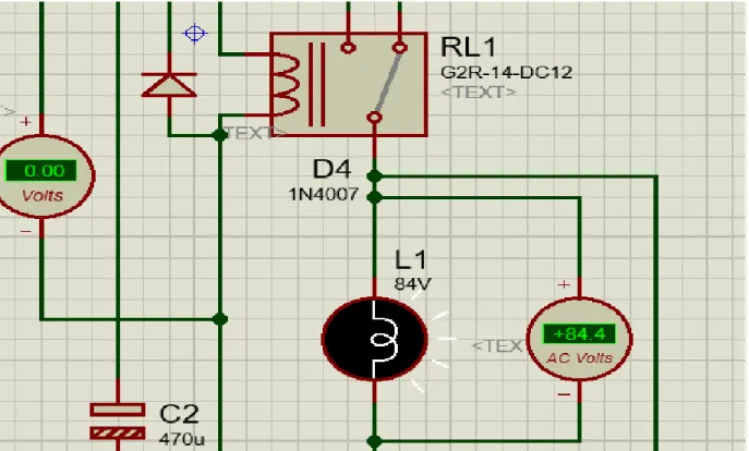
The voltage taken from the voltage divider circuit by resistor R1 and preset resistor VR1; where VR1 is used to set the reference voltage according to the requirement is applied to non-inverting pin 3 of the operational amplifier IC1. When any of the input phase voltages fall below 120 V, the voltage in pin 2 goes high, then the non-inverting pin 3 and the output of the comparator go low. Then the voltage is rectified and filtered using diode and capacitor to get smooth DC voltage.
![Figure 2. 1: Automatic Phase Changer. [3]](https://thumb-us.123doks.com/thumbv2/9docorg/12428402.0/14.918.114.807.110.530/figure-2-1-automatic-phase-changer-3.webp)
Introduction
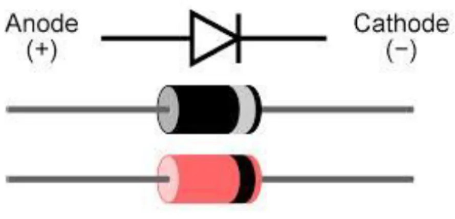
Diode
This means that the diode will only conduct when a positive power supply is connected to the anode (A) terminal and a negative power supply is connected to the cathode (K) terminal, allowing current to flow only in the forward direction. In the opposite direction, the diode blocks any current flowing through it and instead acts as an open switch. Diodes block any current flowing in the reverse direction, or simply act like a short circuit when the current is forward.
![Figure 3. 2: Diode in Forward Bias Condition [7]](https://thumb-us.123doks.com/thumbv2/9docorg/12428402.0/18.918.192.747.267.485/figure-3-2-diode-forward-bias-condition-7.webp)
Zener Diode
- Zener Region
Silicon diode has a very high value for reverse resistance and gives a forward voltage drop of about 0.6-0.7V. They have fairly low values of forward resistance, giving them high peak value for forward current and reverse current.
![Figure 3. 5: Zener Diode [5]](https://thumb-us.123doks.com/thumbv2/9docorg/12428402.0/20.918.220.781.113.248/figure-3-5-zener-diode-5.webp)
BJT
- PNP Transistor
- NPN Transistor
The base-collector junction is reverse biased toward electrons in the base region and holes in the collector region, but forward biased toward holes in the base region; these holes are attracted by the negative potential at the collector terminal. A large fraction of holes in the base region cross the base-collector junction into the collector region, creating a collector current; Conventional current flow is in the direction of hole movement. The base-emitter junction is biased in front of these majority carriers and the electron crosses the junction and appears in the base region.
The property of the core region is that it is very thin, as it is lightly doped with holes. As a result, some recombination occurs with holes, but many electrons are found in the core region. The base-collector junction is biased by the hole in the base region and the electrons in the collector region, but it is forward biased towards the electron in the base region, these electrons are attracted by the positive potential at the collector terminal. A large fraction of the electrons in the base region cross the base-collector junction into the collector region, creating a collector current.
![Figure 3. 8: PNP Transistor [10]](https://thumb-us.123doks.com/thumbv2/9docorg/12428402.0/22.918.262.691.366.543/figure-3-8-pnp-transistor-10.webp)
Operational Amplifier
- Characteristic of an ideal Op-amp (741IC)
- Properties of an ideal Op-amp (741IC)
- Practical Op-amp Circuit
- Voltage Follower (Buffer)
- Inverting Amplifier
- Non-inverting Amplifier
- Summing Amplifier
- Comparator
It is very cheap, especially when you bear in mind that it contains several hundred components. To have different operating characteristics, the op-amp can be connected in a large number of circuits. In this section, some of the most common of these circuit connections will be covered.
The voltage follower circuit, as shown in Figure 3.12, provides a gain of unity (1) without polarity or phase reversal. The output is obtained by multiplying the input by a fixed or constant gain, set by the input resistor R1. The connection in Figure 3.14 has shown an op-amp circuit that acts as a non-inverting amplifier or constant gain multiplier.
Probably the most widely used operational amplifier is the summing amplifier circuit shown in Figure 3.15. The extremely high open-loop gain made the op-amp an extremely sensitive device for checking its input against zero. In Figure 3.16, if V1>V2, the output is directed to a positive supply voltage, and if V2 The switching time from - to + is limited by the slew rate of the op-amp. Using 741 Op-amp as a comparator On a step-up transformer, there are more turns on the secondary coil than the primary coil. Designing it with fewer wire coils on the output compared to the input increases the output voltage proportionally. The induced voltage across the secondary coil is less than the applied voltage across the primary coil or in other words the voltage is "stepped down". When a transformer's secondary voltage is lower than the primary voltage, the transformer is called a step-down transformer. A step-down transformer is one connected such that the supplied voltage is less than the supplied, the actual transformer may be the same in one case as in the other. Their primary voltage is greater than their secondary voltage, this type of transformer "steps down" the voltage on it. For example, a step-down transformer is needed to use 110V equipment in a country where 220V is the usual supply. A step-down transformer usually switches electrical voltage from one level or phase configuration down to a lower level. Step-down transformers are made of two or more coils of stranded wire wound around a core of iron. When voltage is applied to the primary coil, the iron core is magnetized, so a voltage is induced in the other coil. The turns ratio of the two sets of windings determines the amount of voltage transformation. When the operating voltage is applied, the relay coil is energized and the COM contact changes to NO. By using the correct combination of contactors, the electrical relay can be switched on and off. The working principle of a relay can be better understood by explaining the figure 3.24 below. As shown, the electromagnet is connected to the power source using a control switch and via contacts to the load. When current begins to flow through the control coil, the electromagnet begins to energize, thus strengthening the magnetic field. In this way, the upper contact arm begins to attract over the lower fixed arm and thus the contacts close, causing a short circuit to supply the load. On the other hand, if the relay was already off when the contacts were closed, the contact moves in the opposite direction, creating an open circuit. When the power to the coil is turned off, the movable armature will be forcefully moved back to its original position. For low-voltage applications, a higher priority will be given to reducing overall circuit noise. The voltage at non-inverting pin 3 of the op-amp is taken from the voltage divider circuit of resistor R1 and preset resistor VR1 of the variable resistor. Until the supply voltage in one phase is 120V, the voltage at non-inverting pin 3 will be higher than 5.1V at the reference voltage at pin 2, then the output pin 6 will also be high and PNP will remain OFF. If the reference voltage at pin 2 is higher, the voltage at pin 2 will be ON. If the reference voltage on the zener diode will be higher than the voltage on pin 3, then the PNP will turn ON. If the voltage at non-inverting pin 3 is high, then 5.1 V to the reference voltage at pin 2, then output pin 6 will be high and the PNP will remain ON. So the relay will remain de-energized, as soon as the reference voltage at pin 2 is higher, the voltage at pin 2, then the PNP will be ON and the relay will be energized. When the PNP is not conducting, the relay (RL1) remains de-energized and the phase supplies current to the load, leaving the relay in the normally closed (N/C) position. Once PNP is ON, relay (RL1) is energized and the load is disconnected from the phase and connected to the next phase through the next relay (RL2). Summary Voltmeters and Ammeters are used where it is necessary to take the voltage and current for analysis. The figure 4.2 shows the current and voltage ratings at the normal condition for one phase. It is seen from figure 4.2 that in the normal condition each phase carries 3.52A currents for the load of a 25W light bulb. This implies that the circuit is working properly and load-3 is getting the correct voltage level from the healthy power supply line. From the figure 4.3 it is observed that the current through the phase-3 is 0A, which means that the phase of the load is disconnected. Since phase-1 is now connected to load-1 as well as load-2, the current through this phase is increased twice the normal current. When phase-1 is affected it gets correct voltage from phase-2 and when phase-2 is affected it gets correct voltage from phase-3 as we have seen from the main circuit diagram. Let phase-1 is unaffected and phase-2 and phase-3 have voltage less than 120V (For the simulation it was made the affected phase voltage 117V). It can be observed from the simulation that all three phases have correct voltage level under this condition. From Table 4.1 of the simulation result, it is seen that when one or two phases have voltage below 120V, the three-phase loads always get correct voltages (120V, 84.4V rms) at their terminals if any of the three phases are healthy. Limitation of this study Conclusions Directions for the future work![Figure 3. 11: Pin Configuration of 741 IC [6]](https://thumb-us.123doks.com/thumbv2/9docorg/12428402.0/24.918.250.646.398.594/figure-3-11-pin-configuration-741-ic-6.webp)
Transformer
![Figure 3. 18: Transformer [16]](https://thumb-us.123doks.com/thumbv2/9docorg/12428402.0/30.918.175.780.105.435/figure-3-18-transformer-16.webp)
Relay
![Figure 3. 22: Relay [19]](https://thumb-us.123doks.com/thumbv2/9docorg/12428402.0/35.918.363.552.240.397/figure-3-22-relay-19.webp)
Specific work of Transformer, Diode, Capacitor, Zener Diode, Op-amp, BJT and Relay in the main
![Figure 2. 2: Block Diagram of Automatic Phase Changer. [4]](https://thumb-us.123doks.com/thumbv2/9docorg/12428402.0/15.918.131.800.295.859/figure-2-2-block-diagram-automatic-phase-changer.webp)
![Figure 3. 3: Diode in Reverse Bias Condition [7]](https://thumb-us.123doks.com/thumbv2/9docorg/12428402.0/18.918.207.746.711.929/figure-3-3-diode-reverse-bias-condition-7.webp)
![Figure 3. 4: Diode Characteristics [5]](https://thumb-us.123doks.com/thumbv2/9docorg/12428402.0/19.918.203.801.310.654/figure-3-4-diode-characteristics-5.webp)
![Figure 3. 7: BJT [5]](https://thumb-us.123doks.com/thumbv2/9docorg/12428402.0/21.918.111.777.424.714/figure-3-7-bjt-5.webp)
![Figure 3. 9: NPN Transistor [9]](https://thumb-us.123doks.com/thumbv2/9docorg/12428402.0/23.918.233.671.148.370/figure-3-9-npn-transistor-9.webp)
![Figure 3. 14: Non-inverting Amplifier [5]](https://thumb-us.123doks.com/thumbv2/9docorg/12428402.0/26.918.282.694.761.983/figure-3-14-non-inverting-amplifier-5.webp)
