Incorporating Electronics in the Architecture Track of Computer
Science, a Comparative Study
Hassan Farhat [email protected] University of Nebraska at Omaha
Omaha, NE 68182, U.S.A.
ABSTRACT
The latest draft report of the ACM/IEEE Joint Task Force on computer science makes several recommendations1. Of these, for computer architecture: a) a shift towards more use of Programmable Logic Devices (PLDs), and b) more emphasis on the study of power constraints.
While the shift towards use of PLDs requires minimal electrical knowledge, the study of power constraints requires better understanding of the electrical topics. With further constraints placed on the number of credit hours, detailed study the electrical topics may be skipped. The contribution of the paper is to propose a set of electrical topics compiled so as to include under curricula constraints and offer pedagogy of teaching the topics. In addition, the paper presents a comparative study of the electronics topics found in digital design texts2.
1. INTRODUCTION
Digital circuits design is a central topic of study for computer science and computer engineering. The topic spans a range of topics coverage from the high level of computer architecture [18, 19] to the lower level of Very Large Scale Integration (VLSI) [1]. In prerequisites to studying computer architecture, students are required to study digital design [2] to [12] and computer organization [14] to [17].
In 2001, the Joint ACM/IEEE Task Force has recommended a body of knowledge set for the Computer Science field [26]. An interim review with revisions of the report is found in [27]. The latest draft recommendation is found in [28].
In the latest draft report in computer architecture, the recommendation includes the following paragraph: “In this KA, multi-core parallelism, virtual machine support, and power as a constraint are more significant considerations now than a decade ago. The use of CAD tools is prescribed
rather than suggested.” [p. 201]. The report provides a set of guidelines that are not rigid but can be tailored to meet the need of a particular curriculum.
With respect to electrical topics, the shift towards use of programmable logic devices and CAD tools may represent one extreme where electrical knowledge may not be needed. While studying power as a constraint may represent the other extreme where more electrical topics are needed.
To illustrate, we refer to Fig. 1 and Fig. 2. Fig. 1 is a model of a simple computer as a finite state machine with datapath (FSMD).
1 ACM/EEE 2013 ironman draft version
2 Part of this work is presented in IEEE EIT08 conference [23]
Fetch
Decode
Execute inst 1
Execute inst2
Execute inst n Reset
Opcode 0
Opcode 1
[image:1.595.336.497.193.317.2]Opcode n
Fig. 1: Computer as FSMD
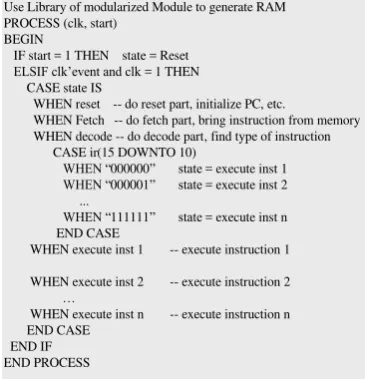
At the behavior level of hardware programming languages, the design of the FSMD can be realized as a nested set of conditional statements (if and case statements), Fig. 2. The figure shows a general behavioral construct for the design in VHDL. In fact, at the behavioral level, a complete design of an accumulator-based computer can be completed in less than 90 lines of code [25]. As can be seen, many of the electrical constrains that may influence the design are left for the computer aided design tools.
[image:1.595.315.498.436.626.2]
Fig. 2: Computer at behavioral level in VHDL
With the above, the computer design is presented as a simple software program with little or no discussion of electrical constraints. For more in depth understanding of the design one can model the computer at the structural level and study the electrical details of the structural units that compose the design. This leads to incorporating in the study, speed and power requirements.
Use Library of modularized Module to generate RAM PROCESS (clk, start)
BEGIN
IF start = 1 THEN state = Reset
ELSIF clk’event and clk = 1 THEN CASE state IS
WHEN reset -- do reset part, initialize PC, etc.
WHEN Fetch -- do fetch part, bring instruction from memory WHEN decode -- do decode part, find type of instruction
CASE ir(15 DOWNTO 10)
WHEN “000000” state = execute inst 1
WHEN “000001” state = execute inst 2 ...
WHEN “111111” state = execute inst n END CASE
WHEN execute inst 1 -- execute instruction 1
WHEN execute inst 2 -- execute instruction 2 …
WHEN execute inst n -- execute instruction n END CASE
In a traditional hardware track in computer science, a digital design course is offered as a first course in the track. At the gate and transistor level, the study requires prerequisites of electrical and electronics concepts acquired through a sequence of classes in electrical engineering. To include the needed electrical topics under number of credit hours constraint is a major challenge to the computer science educator. This is particularly true as found in many digital design texts and under the further added constraints by the ACM/IEEE draft report. To properly understand power consumption, timing delays, and interfacing at the structural level, we need electrical knowledge below the logic gate level.
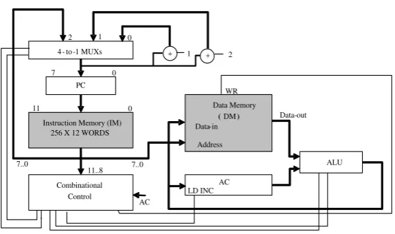
Fig. 3 shows an example of a single-cycle computer designed from several hardware units [20]. In [22] we showed such a design is accomplished using an easy to learn package, Multisim, [13]. A comparative study of computer aided design packages is found in [21]. The need for interfacing study in computer graphics is discussed in [24]. To understand a system electrical details including power consumptions and timing constraints, one needs to understand: a) the electrical properties of the individual units, and b) how they are interfaced.
In earlier work [23], we proposed a set of electrical topics that can be included under curricula constraints. We feel the latest recommendations further support the need to include a set of electronics topics. Our work is related to previous work. We expand on previous work and incorporate power topics discussions. We propose a set of electrical topics to include in a first course in digital design. The topics are proposed so as to complement many of the existing textbooks on digital design. Many of the textbooks lack some of the proposed topics. Either previous knowledge is assumed, or the coverage is not sufficient for a computer science student with no familiarity with electrical topics.
We attempt to present a set of needed topics intended to help the computer science educator in complementing exiting textbooks. Due to the new set of constraints, the educator may choose to cover a subset of the proposed topics. By including the proposed electrical material, the student avoids the need to take additional courses in electrical and computer engineering. To aid and speedup the learning process, extensive use of Multisim (software package) is incorporated. This accelerates the learning process through circuit simulation at the electrical level and, hence, avoids the time consuming process of actual design.
The paper is organized as follows. Section 2 includes, the needed electrical topics. These topics are compiled so as to better understand the electrical properties of logic gates and assume the student had no previous knowledge in electricity. In the remaining sections, we propose teaching methodology samples of the topics in the context of theory and Multisim. In section 3, we discuss how to incorporate Transistor-Transistor-Logic (TTL) and interfacing in Multisim. In section 4 we discuss power consumption as it relates to TTL and data sheets. Based on Moore’s law, as the number of circuit elements increases exponentially, power constraints become more important in design decisions. Sections 5 and 6 deal with the need for alternative designs to cope with power constrains. The sections cover Complementary Metal Oxide Semiconductor (CMOS) technologies. In section 7 we include a comparative study of the electrical topics found in popular existing digital design textbooks. The intention of the comparative study is to aid the new educator. The conclusions are given in section 8.
2. THE ELECTRICAL TOPICS GROUPS
Logic circuits are designed using two dominant technologies: transistor-transistor-logic (TTL) and complementary metal-oxide-semiconductor (CMOS). To accommodate the various design platforms (handheld devices, laptops and desktops for example) CMOS designs are offered based on different voltage sources. These include the traditional 5 V technology and the low-voltage CMOS technology (3.3 V, 2.5 V, and 1.8 V).
Today digital designs incorporate different technologies in realization of a digital system. To understand the interfacing requirements and other electrical constraints in design, a designer refers to a unit data sheet. As a result, in considering the proper electrical coverage, an important minimal objective is the need to understand and interpret the various data sheets of primitive elements in combinational and sequential circuits. We compiled a sample of needed topics as presented in Table 1.
The table is composed of 5 groups. Based on the students background some groups maybe skipped. As can be seen in the table, group 1 covers the basic level, Ohm’s law. Some textbooks may start at this level. However, the textbooks may not be thorough enough as they may assume previous experience with electrical and electronics concepts leaving gaps in understanding the design process.
[image:2.595.167.455.75.245.2]
Fig. 3: Schematic of the single-cycle computer
4 - to -1 MUXs
PC
Instruction Memory (IM) 256 X 12 WORDS
Combinational Control
Data Memory (DM)
Data-in Address
AC LD INC
ALU +
+ 1 2 0
1 2
0 7
7..0 0 11
AC 7..0
11..8
WR
Group 2 covers three basic important semiconductor elements diodes, Bipolar Junction Transistors (BJT) and Metal-oxide-semiconductor Field-effect transistor (MOSFET). For gate design, the general functions of the semiconductor components are covered as non-linear devices. We then cover first order approximation of devices.
Table 1: Sample topics coverage
In group 3 we consider design of the basic logic gates. Each gate design is considered in the different technologies, diodes, Transistor-Transistor-Logic (TTL), N-channel MOS (NMOS) and complementary MOS (CMOS). The group also considers realization of important gates with non-logic outputs such as tristate and open-drain. It includes as well coverage of transmission gates used in discussion of multiplexer circuits. To understand data sheets we then study the input-output characteristic of the inverter circuit.
With the discussion of the previous groups, interpreting data sheets can be covered clearly. In particular, voltage and current constraints can be covered as related to actual designs. Further, based on the discussion of group 3, students can perform actual computations of the different data columns found in data sheets. This includes, the columns for VOH(min), VOL(max), VIH(min) and VIL(max). It also includes computations of currents into and out of logic gates. Based on the concepts of the current and voltage computations, further important discussions can be carried (fanouts, speed, power dissipation, and noise margins). Additional power dissipation concepts can be discussed (statistic and dynamic) where the load model can be a resistor as in TTL designs or a capacitor as in CMOS designs.
In the final group, interfacing, we cover interfacing by first discussing interfacing of chips from the same technology and series. We then cover interfacing between different series. Interfacing between different series is important given the many low-voltage chips provided by CMOS. We then discuss input and output interfacing. This includes switch and LED interfacing which includes load resistors computations. The final topic in the group is discussion of startup issues where initial memory element values (flip-flops) can be covered.
3. USING MULTISIM
We use Multisim to simulate electrical circuits designs. Simulation avoids the time consuming process of performing actual design. The software has an easy to use graphical user interface where design and simulation can be performed using the same interface. The package can simulate designs from simple RC circuits to simple computer designs [22]. Using simulation helps the students: a) concentrate on concepts, and b) verify these concepts; resulting in a faster learning process.
We illustrate the use of the package in five applications: 1) circuit response to an RC circuit and simulated oscilloscope; 2) load line construction of a common-emitter bipolar junction transistor; 3) transistor-collector characteristic curves; 4) input-output voltage transfer curves of a TTL inverter; and 5) interfacing. The five concepts are clarified significantly when simulated. This is especially true for a computer science student with no formal background in electrical and electronics circuits.
The RC circuit simulation: For discussion of group 1
[image:3.595.339.493.311.403.2]example we look at Fig. 4 designed in Multisim. The circuit shows an RC circuit with a switch. By pressing the spacebar on the keyboard, the SPDT switch can be connected to the R2 resistor or to the positive side of the voltage source. Hence the circuit can be used to simulate charging and discharging the capacitor C1. The circuit can be used to enforce the concepts of measuring RC constants (approximately 0.63 VCC). This is illustrated in Fig. 5 where the RC circuit response is shown using a simulated oscilloscope. The figure shows two time bars that can be moved to read the RC constant value.
Fig. 4: Using Multisim to simulate RC circuit response
Fig. 5: Simulated Oscilloscope response
Load line construction: Fig. 6 shows an example circuit
in Multisim. The design is of a common emitter Bipolar-Junction Transistor (BJT) circuit with several SPT switches and ammeters. The circuit can be used to verify the load line construction concepts from group 2. Here the VCC voltage is fixed through the use of the switches labeled A through J while the IB values are changed using the switches labeled 0 through 9 (the IB value changes due to the different resistors). The corresponding IC and VCE values are read on the simulated ammeters and voltmeters, respectively.
R1 10k
V1 12 V
C1 1 uF Space
R2 20k
VC = 12 V, IC = 0 Group 1: Basic Electricity Group 2: Semiconductor Elements Function and Characteristics
Ohms law Diodes, Light-emitting diodes, seven segment displays Kirchhoff's laws Bipolar junction transistor
Mesh analysis MOSFET, NMOS, PMOS
RC circuits Characteristics curves Thevenin equivalent First order models Group 3: Logic Gate Design Group 4: Interpreting Data sheets Diode, TTL and CMOS design Fan-outs
Open-drain and tristate design Power dissipation (dynamic and Statistic) Input-output transfer characteristics Noise margin
Transmission gates Speed
[image:3.595.324.510.449.589.2]Fig. 6: Use of circuit in characteristic and load line concepts
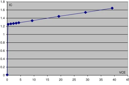
Transistor-collector characteristic curve: Fig. 6 can be
used, as well, to generate transistor-collector characteristic curves by fixing the IB value and adjusting VCC so as to obtain different VCE values. Fig. 7 shows the result using Excel.
Voltage transfer curves of a TTL inverter: In Fig. 8 we
[image:4.595.311.520.71.300.2]construct the design of a standard TTL NAND gate. The design can be converted to an inverter gate by connecting the two inputs to generate a single input circuit. The circuit can be used to form the input-output characteristic curves found in group 3. This is done by adjusting the input voltage values, and reading the corresponding output voltage values. On plotting voltage values we obtain the input/output characteristic curve shown in Fig. 9.
[image:4.595.323.525.408.535.2]Fig. 7: Transistor-collector characteristic curve
Fig. 8: Simulated NAND gate
Interfacing: An example of Multisim use from group 5, interfacing, is shown in Fig. 10. The figure shows interfacing of 2 V logic to 5 V logic. For the driver HIGH output (Fig. 10 (b)) the HIGH output is not recognized as a HIGH by the load (U6). As a result, the circuit response is the same for both inputs (Fig. 10 (a) and (b)).
Fig. 9: Sample input/output characteristic curve
U1A
74HC00D_2V
GND VDD 2V
1.5V
2.000 V +
-U6
NAND2 X2
2.5V
5.000 V +
-Circuit-interfacing
X1
Fig. 10 (a): Input 1; output of U1A = 0V (logic 0) and output of U6 = 5V
1k VDD 5V
B
-3.469nA +
-0.057mA +
-0.057mA
+ - +0.022 V
-0.606 V +
-0.583 V + -1M
0
500k
1
500k
2
500k
3
500k
4
200k
5
100k
6
50k
7
10k
8
1k
9
K F G H I J
V1
3 V V2
5 V V3
10 V V4
15 V V5
20 V V6
30 V
Q2
2N390 4
A C D E
V7
0 V V8
0.5 V V9
1 V V10
2 V
0 0.2 0.4 0.6 0.8 1 1.2 1.4 1.6 1.8
0 5 10 15 20 25 30 35 40 45
VCE IC
5V VCC
5V VCC
A
B
0.023 V + -Q1
Q1
Q2
Q3 Q4
130 1.6
4 k
0.888uA + -0.726mA
+
-output
1k
R1 R2 R4
R3
3.145mA + -0.789 V + -3.359mA +
-2.632mA +
-k
Voltage Transfer Curves
0 1 2 3 4 5
0 1 2 3 4 5 6
Voltage IN
V
o
lt
a
g
e
o
u
[image:4.595.74.281.524.661.2] [image:4.595.315.531.573.682.2]U1A
74HC00D_2V
GND VDD 2V
1.5V
2.000 V +
-U6
NAND2 X2
2.5V
5.000 V +
-Circuit-interfacing
X1
Fig. 10 (b): Input 0; output of U1A = 2V (logic 1); output of U6 should be 0V (logic 0)
We expand next on discussion of power consumption as presented in group 4. Based on the ACM/IEEE task force [28], more emphasis is placed on power consumption.
4. POWER CONSUMPTION CONSTRAINTS
With the increase in switching components on a VLSI chip and the increase in components with processing units, the latest ACM/IEEE recommendations include coverage of power consumption topics.
Consider Fig. 11. In order for a digital circuit to work, it requires a certain amount of electrical power. When a digital circuit uses power to operate, we say the circuit dissipates (or consumes) power. We use the figure in illustrating power constraints. By definition the power consumed by the circuit is P = VCC . ICC.
Fig. 11: Example circuit for power discussion
Multisim can be used to speedup the discussion of power consumption. We illustrate how power consumption can be computed as applied to TTL, in particular the NAND circuit shown in Fig. [9]. TTL data sheets supply two types of currents ICCH and ICCL, corresponding to current demands on output HIGH and LOW, respectively. The currents are given based on open circuit outputs; that is no load is connected to the output. Three columns for current are given, minimum, typical and maximum.
Normally the currents are different. Power dissipation is based on the average current . The
average power dissipated is . In computing ICC, the column for typical current is used. Data sheets provide power dissipation as well, 40
mW/chip. The power dissipation as well as the current values can be verified and theoretically computed using Multisim (refer to Fig. [9] where ICC is read below the VCC value). The power computation is computed as
(1)
where n is the number of gates on a chip.
The need for alternative design technology is then discussed based on the increase in number of switching elements based on Moore’s law (predication). With the number of switching elements exceeding 2 billion elements, this leads to today’s CPU designs using Complementary Metal Oxide Semiconductor (CMOS).
5. METAL OXIDE SEMICONDUCTOR TRANSISTORS
Here we discuss the Metal Oxide Semiconductor (MOS) transistor. In the next section we propose discussion of dynamic power in the context of the proposed topics coverage.
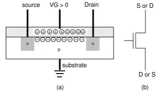
Fig. 12 shows a 2D view of a MOS transistor (Enhancement-Mode Metal-Oxide-Semiconductor Field-Effect-Transistor, E-MOSFET).
[image:5.595.74.289.70.181.2]
Fig. 12: n-type E-MOSFET Transistor
[image:5.595.313.527.177.263.2]Similar to a TTL transistor, the circuit is composed of three inputs (source, gate and drain). We show a 3D view of the gate. The gate is characterized by a length and width. It is surrounded by an insulator (SiO2, glass) as shown in Fig. 13.
Fig. 13: 3D view of gate part of E-MOSFET transistor
In the discussion, brief explanations are made about the transistor as a controlled switch that connects the source to the drain. The gate input functions as the switch control. This is shown in Fig. 14 part (b). In part (a) the insulator material results in a capacitor model between the substrate and the gate. By applying a positive voltage on G we induce a negative channel of electrons in substrate below the gate. This results in a closed switch by inducing a conduction path from source to drain. Similarly, a 0 voltage on the gate input removes the conduction path and keeps the switch open.
Fig. 14: (a) Capacitor effect, MOSFET with conducting
channel, (b) MOSFET as a switch
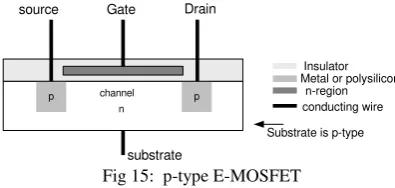
The above transistor design is called n-type E-MOSFET (abbreviated as nMOS). The n is used to indicate that conduction is due to negative carriers. Similar design can be completed with the substrate semiconductor of type n, the gate and source of type p, resulting in pMOS, Fig. 15.
Electrical or Digital Circuit ICC
VCC
2 )
( CCH CCL
CC
I I avg
I
CC CC
D avg I avg V
P ( ) ( )
CC CCL CCH
D V
I I n avg
P
2 )
(
n n
source Gate Drain
p
substrate
Insulator Metal or polysilicon n-region conducting wire
Substrate is p-type channel
Gate
L W
Insulator (Si02)
n n
source VG > 0 Drain
p
substrate ++ ++ ++++ –––––––––
+
S or D
D or S
[image:5.595.312.530.358.395.2] [image:5.595.113.235.380.436.2] [image:5.595.335.499.552.646.2]Fig 15: p-type E-MOSFET
We discuss next power consumption in CMOS circuits
6. DYNAMIC POWER CONSUMPTION
Consider Fig. 16. The figure represents the design of a NAND gate in CMOS. The design is called CMOS (Complementary Metal Oxide Semiconductor) since the design incorporates both nMOS and pMOS transistors (alternative designs that use nMOS only use more power are not as common). In the figure, alternative switch representation for the two types are shown in Multisim. We introduce dynamic power to the students by breaking the design, as is customary, into two networks, a pull-up and a pull-down networks. The pull-up network is composed of the pMOS transistors Q1 and Q2. Similarly, the pull-down network is composed of the nMOS transistors Q3 and Q43.
By inspecting all steady state input combinations we show that at no time, there is a direct path from the power source (VDD for CMOS circuits) to ground. As a result, the current is 0 (the gate substrate forms a capacitor; the steady state current gate current is 0). Hence the power dissipation is approximately zero. We contrast this with the TTL alternative design of the NAND gate. The power consumed when the gate inputs/outputs are not changing is called static power dissipation. Hence, we emphasize the advantage of CMOS over TTL in terms of static power consumption.
Fig. 16: (a) CMOS design of a NAND gate, (b) NAND gate
We then introduce and compute dynamic power consumption. In designs of CMOS circuits, dominant power loss is due to dynamic power4. This occurs as the gate inputs/outputs are changing. When interfacing TTL circuits, the dominant model used is a load resistor. When interfacing CMOS circuits, however, the dominant model used is a capacitive load.
3 The transistors symbols show alternative transistors representation.
In capacitive loads, the steady state current is zero. This part of the discussion can be illustrated by referring to the RC circuit (Fig. 4 and Fig. 5). The capacitor can be considered as the load capacitance. In such a circuit, the steady state current is 0 since the capacitor voltage is 12 V or 0 V (capacitor is fully charged (switch connected to 12 V) or fully discharged (switch connected to R2)). Hence, in this mode, after charging the capacitor, the power consumed is 0 W. This is not the case if a resistor replaces the capacitor simulating a TTL circuit.
While minimal power is consumed in steady state, CMOS circuits consume power as the capacitive loads are charging. For CMOS gates, the load inputs are modeled as capacitors (first order approximation). While a capacitor is charging, the consumed power is called dynamic power
consumption, P(t) = VDD IDD(t) (IDD is used for CMOS). For an RC circuit, the current IDD is a function of time as indicated in the equation. Hence one is interested in the average power consumption over a time interval, T. The average power can be computed using the equation
(2)
With (3)
(VC is the capacitor voltage, and Q = C VC is the charge accumulated on the capacitor) we obtain
(4)
Hence (5)
Assuming the capacitor, was fully discharged at time 0 and fully charged at time T, we have VC(0) = 0 and VC(T) = VDD. The total energy delivered to the RC circuit by the
power supply is (6)
Equation (5) for power consumption is called dynamic since it is a function of charging/discharging the capacitor. Once this is done, since the current IDD is reduced to 0 A, no additional power consumption is caused. If the output is changing at a frequency, f, then the total dynamic power consumption can be computed as follows. Over one period of time T, the capacitor charges (output transition from 0 to 1, and then discharges, transition from 1 to 0 (no energy is delivered to the circuit by VDD). Hence, for a circuit with outputs changing at a rate, f, the dynamic power consumed is
(7)
The power consumed by a CMOS circuit is dominated by dynamic power consumption. To illustrate this we look at the ALVC 7400 package for example. It contains 4 NAND gates, designed using low power CMOS with VDD = 3 V. The typical current supplied to the package is 2.5 A per gate. Hence the typical power consumed is
P = VDD ICC = 3 V 2.5 A = 7.5 W
4Today, due to the thin gate oxide insulator, leakage currents
play important roles as well.
p p
source Gate Drain
n
substrate
Insulator Metal or polysilicon
n-region conducting wire
Substrate is p-type channel
5V VDD
5.000 V +
-Q3 Q1
Output Q2
Q4 Inputs
(a)
(b)
A
B
Pull-up Network, pMOS transistors
Pull-Down Network, nMOS transisotors
T T
DD i tdt
T V dt t p T Paveg
0 0
) ( )
( 1
c c
c dt CdV
dt V d C dt dt CV d dt dt dQ dt t
i() ( ) ( )
( ) (0)
)(
0 0
c c DD T
c DD T
DD V T V
T CV dV T CV dt t i T V
Paveg
T CV dV T CV dt t i T V
Paveg DD
T c DD T
DD 2
0 0
)
(
2 2 )
( DD CVDD
T CV T t
E
2
DD dynamic f C V
When compared to the power consumed by TTL, TTL uses over 1000 times more static power than CMOS.
The power consumption values are based on the output of a gate connected to a standard capacitive and resistive load. To account for dynamic power consumption we need to use the CV2 equation. As a result, knowledge of the C value is needed. In addition, one needs to know how often the output is changing. Alternatively, one can use a current rating found in the data sheets, ICC. This represents the current as a result of charging the load capacitor. To compute the dynamic power consumed we use P = VCC
ICCf, where f represents the fraction of time the output is changing.
7. COMPARATIVE STUDY OF TEXTBOOKS
We looked at several textbooks in the field to determine the electrical coverage in each. None of the textbooks covered all the topics found in group1. Outside group 1 and semiconductor characteristic, [12] is the most comprehensive. For transmission gates coverage, [7] provides the best coverage. For interfacing and sizing the resistor values, [8] provides very detailed discussion. Ref. [8] also devotes: a) a special chapter “Practical consideration for Digital Design”, b) a chapter on interfacing to analog devices, and c) an appendix on basic electricity. We feel the basic electricity discussion is incomplete (KVL, KCL, and RC circuits discussions are missing for example).
Ref. [11] contains good introductory discussion of CMOS design at the layout level. The textbook skips TTL discussions and does not contain data sheets and logic interfacing discussions.
Ref. [9] includes good coverage of both TTL and CMOS circuits. It also contains a good discussion on characteristic curves. Ref. [9] is a classical text on the topic but assumes previous knowledge in electricity and does not include data sheets discussion. Ref. [10] is a good textbook that is comparable to [8]. Ref. [3] assumes previous knowledge in basic electricity and semiconductor technology. Otherwise the textbook provides detailed and practical discussion on digital electronics topics.
We think the combination of [12] and [11] provide the most comprehensive discussions. Ref. [12] provides the best digital electronics topics. Ref. [11] provides the best coverage on semiconductor technology.
8. CONCLUSION
In this paper we presented a set of electrical topics that can be included in the architecture track of computer science. With the latest ACM/IEEE task force recommendation, more discussion can be devoted to power constraints. We proposed coverage of the topics in Multisim. We also presented a brief comparative study of textbooks in the field. The proposed work is intended in helping the computer science educator; it incorporates a set of electric concepts under the computer architecture track. With the increasing power constraints the trend is to concentrate discussions on CMOS circuits.
9. REFERENCES
[1] N. Weste and D. Harris, “CMOS VLSI Design: A Circuits and Systems Perspective 4th edition”, Addison Wesley, 2011.
[2] S. Brown and Z. Vranesic, Fundamentals of Digital Logic with VHDL Design with CD-ROM, 3rd edition, McGraw-Hill, 2009.
[3] N. Cook, Digital Circuits with PLD Integration, Prentice Hall, 2001.
[4] A. Dewey, Analysis and Design of Digital Systems with VHDL, PWS publishing, 1997.
[5] T. Floyd, Digital Fundamentals: A System Approach, Prentice Hall, 2013.
[6] D. Gajski D, Principle of Digital Design, Prentice Hall, 1997.
[7] R. Katz and B. Gaetano, Contemporary Logic Design, 2nd edition, Prentice Hall, 2005.
[8] W. Kleitz, Digital Electronics A Practical Approach with VHDL, 9th edition, Prentice Hall, 2012.
[9] M. Mano, Digital Design, 3rd edition, Prentice Hall, 2003.
[10] R. Tocci, N. Widmer and G. Moss, Digital Systems Principles and Applications, 11th edition, Prentice Hall, 2011.
[11] J. Vyemura, A First Course in Digital Systems Design an Integrated approach, Brooks/Cole, 2000.
[12] J. Wakerly,Digital Design Principles and Practices 4th edition, Prentice Hall, 2006.
[13] Electronics Workbench,
www.electronicsworkbench.com
[14] J. D. Carpinelli, Computer Systems Organization and Architecture, Addison-Wesley, 2000.
[15] D. Patterson and J. Hennessy, Computer Organization and Design, Revised 4th edition, Morgan Kaufmann, 2011. [16] W. Stallings, Computer Organization and Architecture, 9th Edition, Prentice Hall, 2013.
[17] D. Harris and S. Harris, Digital Design and computer Architecture, Morgan Kaufman, 2007.
[18] J. P. Hayes, Computer Architecture and Organization 3rd edition, McGraw-Hill, 1998.
[19] J. Hennessy and D. Patterson, Computer Architecture: A Quantitative Approach 5th Edition, Morgan Kaufmann, 2011.
[20] H. Farhat, “Integrating Hardware and Software in Early Research in Computer Science”, Proc. ISCA CAINE, Honolulu, Hawaii, USA, 2005, pp. 390-394.
[21] H. Farhat, “A comparative study of Max+PLUS II and Quartus schematic capture tools”, International Conference on Systems Engineering, 2006, pp. 119-124.
[22] H. Farhat, “An interactive computer Design in Multisim”,Proc. ISCA CAINE, 2008.
[23] H. Farhat, “Integrating Electronics in Computer Science under Curricula Constraints, a Comparative Study”, IEEE International Conference on Electro Information Technology, 2008.
[24] H. Farhat, “Incorporating Output Interface in Studying Computer Graphics in Computer Science”, to appear Proc. FECS, 2013.
[25] J. Hamblen and M. Furman, Rapid Prototyping of Digital Systems, a tutorial approach, Kluwer Academic Publishing, 2001.
[26] http://www.acm.org/education/curric_vols/cc2001.pdf
[27]http://www.acm.org/education/curricula/ComputerSci ence2008.pdf
[28] http://ai.stanford.edu/users/sahami/CS2013/