heterojunction of Si/SiGe axially heterostructured
nanowires under laser illumination
Jose Luis Pura1, Juli´an Anaya2‡,Jorge Souto1, ´Angel Carmelo Prieto1, Andr´es Rodr´ıguez3, Tom´as Rodr´ıguez3, Juan Jim´enez1
1GdS Optronlab, Dpt. F´ısica de la Materia Condensada, ed. i+d, Parque Cient´ıfico, Universidad de Valladolid, Paseo de Bel´en 1, 47011 Valladolid, Spain
2Centre for Device Thermography and Reliability, HH Wills Physics Laboratory, University of Bristol, Tyndall Avenue, BS8 1TL, Bristol, UK
3Ingenier´ıa Electr´onica, ETSI de Telecomunicaci´on, Universidad Polit´ecnica de Madrid,Avenida Complutense 30, 28040 Madrid, Spain.
Abstract.
We present a phenomenon concerning the electric field enhancement at the heterojunction region of axially heterostructured Si/SiGe nanowires when the nanowire is illuminated by a focused laser beam. The electric field is sensed by micro Raman spectroscopy, which permits to reveal the enhancement of the Raman signal arising from the heterojunction region; the Raman signal per unit volume increases at least 10 times with respect to the homogeneous Si, and SiGe nanowire segments. In order to explore the physical meaning of this phenomenon, a 3-dimensional solution of the Maxwell equations of the interaction between the focused laser beam and the nanowire was carried out by finite element methods. A local enhancement of the electric field at the heterojunction was deduced; however, the magnitude of the electromagnetic field enhancement only approaches the experimental one when the free carriers are considered, showing enhanced absorption at the carrier depleted heterojunction region. The existence of this effect promises a way to improve the photon harvesting using axially heterostructured semiconductor NWs.
1. Introduction
Semiconductor nanowires (NWs) are attracting a great deal of attention because of the increasing number of potential applications based on their unique properties.[1] Most of these properties arise from the NW confined dimension, the diameter, as compared to some characteristic lengths, e.g. exciton Bohr radius, phonon mean free path, wavelength of the incident electromagnetic (EM) waves, etc.[2] In particular, there is a great interest in the interaction between semiconductor NWs and light,
‡ Corresponding Author
as their optical properties make of them the optimal candidates for nanophotonic devices.[3][4] A broad range of unique optical properties of semiconductor NWs have been reported, e.g. waveguiding,[5] optical resonances,[6] antenna effects among others.[7] All these effects emerge because light interacts with the NWs in different ways depending on the NW diameter, wavelength, and dielectric properties of the NW and the surrounding media. One of the most relevant properties concerning the light/NW interaction is the ability of NWs to enhance their optical absorption/scattering for certain diameters, which are characterized by large local electric fields inside the NW.[8] The absorption/scattering resonances deal with different phenomena recently reported, including, among other, the enhanced photocurrent response of the NWs,[7] enhanced elastic and inelastic light scattering by Si NWs,[9] light extinction,[10] light emission in different semiconductor NWs,[11][12] and second harmonic generation.[5] Since the Raman intensity is proportional to the excitation light intensity and the scattering volume, the experimental study of the interaction of light with matter at the nanoscale can be carried out by its Raman response.[13] This makes of Raman spectroscopy an excellent probe for sensing the local electric field induced inside the NW under incident light. In addition, it is possible to take advantage of its capabilities as a powerful non-destructive technique for the characterization of the structure, composition, stress, thermal, electronic, and optical properties of semiconductor NWs.[6][14][15][16][17][18] It is worth noting that up to now the research interest about the light/NWs interaction has been focused mainly on homogeneous single NWs and/or core-shell heterostructured NWs;[19] however, the response of axially heterostructured NWs to the electromagnetic waves is still unexplored. These kind of structures are attracting an increasing interest since heterojunctions (HJ) are necessary for the development of semiconductor NW based devices.[20] In the junction of these NWs a jump in the complex refractive index due the abrupt change of materials is expected, which therefore may change the electromagnetic (EM) response of the NW. Besides the HJ built-in electric field, which can locally change the polarizability, the oscillator strength and the presence of free carriers, either native or photogenerated, could also affect the electric field distribution inside the NW. To further advance in this subject, we present in this work a study of the distribution of the electromagnetic field in axially heterostructured Si/SiGe NWs, paying special attention to the role of the HJ in the optical response of the NW. This is carried out experimentally by using its Raman response as a sensor of the local electric field. The experimental data are compared to the output of a 3 dimensional (3D) solution of the Maxwell equations characterizing the electromagnetic laser/NW interaction by finite element methods (EM-FE), enabling to explain the role of the HJ in the EM interaction.
2. Experimental description and samples
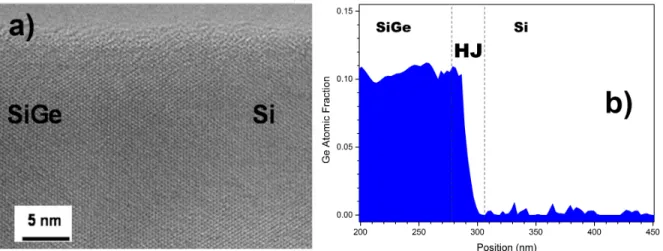
Figure 1. a) High resolution TEM image of the HJ. b) EDX Ge atomic fraction profile across the HJ.
compositions as catalysts. The as-grown NWs were sonicated in an ultrasonic bath and suspended in methanol; subsequently the NWs were deposited on an Al substrate by drop-casting. For more details about the growth of these NWs see refs [21] and [22]. High resolution transmission electron microscopy (TEM) and energy dispersive X ray (EDX) analyses of the HJ was carried out. High resolution TEM images of the HJ region of SiGe/Si HJs did not show structural discontinuities at the junction, nor stacking faults, or other structural defects, Fig.1a. The EDX profile shows a compositionally graded HJ with a width of around 30 nm, of the order of the NW diameter, ≈ 32 nm for the NW shown in Fig. 1b.
The micro Raman spectra of several individual Si/SiGe NWs were recorded with a high resolution Labram UV-HR 800 Raman spectrometer from Horiba-JovinYvon. The excitation and the scattered light collection were performed by means of a confocal metallographic microscope with a high magnification objective (100X and 0.95 numerical aperture (NA)). The excitation was done with a frequency doubled Nd:YAG laser (532 nm). The measured laser beam diameter at the focal plane for these conditions is∼1µm, thus slightly bigger than the ∼700 nm given by the Abbe’s criteria (w0 ∝ 1.22λ/N A)
permits to localize the HJ, and also to study the Raman intensity profiles along the NW, and more interestingly around the HJ.
3. Experimental results
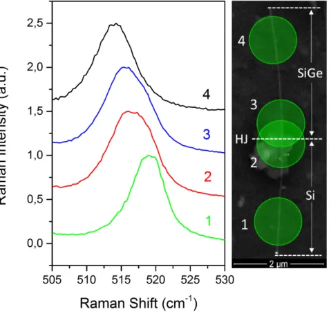
Four Raman spectra recorded at different positions along an axially heterostruc-tured Si/SiGe NW are shown in Figure 2. Spectrum 1 was taken on the Si segment of the NW, while spectrum 4 was recorded on the SiGe segment. Spectra 2 and 3 were recorded with the laser beam sharing the two pure segments and the HJ. When these spectra are compared, a dramatic change is observed in the spectral shape of 2 and 3 with respect to 1 and 4. Spectra 1 and 4 show a typical Lorentzian peak, with the spectral parameters characteristic of Si and Si0.9Ge0.1 NWs respectively.[24][25]
Mean-while, the spectra recorded in positions 2 and 3 appear broadened and asymmetric, as a consequence of the overlapping contribution to the Raman spectrum of the different regions of the NW being simultaneously excited by the laser beam. In order to analyze this signal, spectral deconvolution shall be thus carried out to ascertain the different contributions of the pure Si and SiGe segments of the NW, and also the contribution of the HJ region. For this deconvolution we used the spectra 1 and 4, corresponding unequivocally to the Si and Si0.9Ge0.1 pure NW segments, as the reference spectra for
the fitting of the spectra 2 and 3. However when using a weighted Gaussian convolution –from the focused laser intensity distribution– of the two bands corresponding to the two pure segments it is not possible to reproduce the Raman recorded when the laser beam is sharing the three NW regions, i.e. spectra 2 and 3 (see Fig.3 inset).
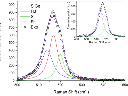
Fig. 3 shows that a third band is necessary to achieve a satisfactory fit of the spectra recorded with the participation of the HJ, e.g. 2 and 3. This third contribution, which has a peak width and frequency intermediate between those recorded for the pure Si and Si0.9Ge0.1 NW segments, should arise exclusively from the very narrow HJ
region. It should be noted that the HJ region in VLS NW growth does not present a sharp composition change, but it follows a compositionally graded transition from the nominal 10% Ge of the SiGe segment to the pure Si segment (see Fig.1a). The thickness of this transition region is of the same order of magnitude of the NW diameter, and it is consequence of the Ge reservoir effect on the catalyst droplet. Once the GeH4 gas
Figure 3. Fitting of the Raman signal corresponding to an intermediate composition between the two NW segments, a satisfactory fitting can only be achieved by using a third Raman band. (Inset) Fitting of a Raman spectrum sharing the three NW regions using only two bands with the spectral parameters of the Raman bands of the pure Si and SiGe segments respectively, this fitting neglects the contribution of the HJ.
Figure 4. Intensity profiles along the NW axis for the overall Raman signal and for the deconvoluted bands corresponding to the three regions of the NW, showing the enhancement under the influence of the HJ. The points correspond to the positions of the laser beam center where the Raman spectra were recorded. The data have been normalized to the one corresponding to the pure Si region to better illustrate the enhancement in Raman signal.
4. Laser/NW interaction by finite element method (EM-FEM) simulations
To study the quantitative interaction between the focused laser beam and the NWs, and thus to unravel the distribution of the electromagnetic field inside the HJ NW, one needs to solve the Maxwell equations for the laser/NW system. This has been typically carried out by means of the Lorenz-Mie theory, in which the NW is described as an infinitely long cylinder immersed in a homogeneous and isotropic non absorbing medium.[28] In the frame of this formalism, the calculation of the absorption, and scattering efficiencies,
QabsandQsc respectively, has revealed a strong dependence of these coefficients with the
presence of the HJ, the simulation of the axially heterostructured NWs cannot be performed by a 2D approach like the ones typically used when studying the light/NW interaction for homogeneous NWs and core-shell heterostructured NWs.[14][15] Instead, here we solved a 3D model accounting for the axial HJ and the finite length of the NW, as well as the presence of the metallic substrate. The electromagnetic model used here reproduces a HJ-NW with the same characteristics as the one shown in Fig. 4, deposited on a metallic (Al) substrate and surrounded by air. The NW is illuminated by the same 532 nm Gaussian laser beam used in the experiments. The air/NW/substrate system was limited by Cartesian perfectly matched layers (PMLs), which absorb all the outgoing radiation, thus eliminating secondary reflections on the boundaries. The complex refractive indexes were obtained from Sopra database.[30] In a first step the response of a perfectly dielectric NW was calculated. This model was solved for different positions of the excitation laser beam along the NW axis in order to reproduce the experimental profile of Fig. 4. A particular solution of the model is shown in Fig.5, where one observes the 3D distribution of the relative electric field intensity, defined as E2
r =|E|2/|EIncident|2 (i.e., the electric field enhancement over the
incident laser electromagnetic field), inside the heterostructured NW. In the same figure we also included the profile of this magnitude along the NW axis, highlighting the local enhancement at the HJ region. For each position of the laser beam the electromagnetic field distribution inside the NW is calculated. The volume integrals of the square of the electric field, |E|2, in the three different regions: Si segment, SiGe segment and the HJ,
are then calculated. The value of these integrals should therefore be proportional to the theoretical Raman signal arising from each NW region under the excitation beam.[13] It is remarkable that this model shows a similar amplification and localization of the EM field in the HJ region, see Fig.5; however, the estimated amplification for the HJ region was lower than the one deduced from the experimental data (see Fig 6, pink dots). In order to explain this discrepancy, a more complete model accounting for the effect of the photogenerated carriers in the solution of the Maxwell equations was considered. This is needed since the presence of free carriers will contribute to the dielectric losses. For the excitation conditions of our measurements and a surface recombination velocity (SRV) of S ≈ 3 105 cm/s,[31] it results in a photogenerated carrier concentration of
Figure 5. 3D representation of a solution of the model for a similar heterostructured NW than the ones experimentally studied. A magnification of the HJ region with the
E2r relative intensity axial profile showing enhancement at the HJ is also represented.
Once the free carriers were considered the model was solved for a carrier density ranging from 1016 to 1020cm−3. The results obtained for two representative carrier
densities, n = 8 1018cm−3 and n = 5 1019cm−3, are shown in Fig. 6. From here it is clear that by including the effect of the photogenerated carriers in the model, the electric field is strongly localised in the HJ region, well approaching the contribution observed in the experimental data of Fig.4, and therefore explaining the origin of anomalous effect observed in the experiments. However we should note that the experimental intensity of the SiGe segment is higher than the intensity measured for the Si segment, as opposed to what is observed in the EM-FEM model, which shows similar values for both segments. This discrepancy might arise by a difference of a few nanometers in the diameter of both segments, which due the diameter dependent resonance in the Raman intensity, can be responsible for the observed difference;[29]in fact, diameter changes in the presence of axial HJs are common. Here to simplify the problem, the data of Fig. 6 were calculated for an ideal cylindrical NW, without diameter change and therefore the model do not account for these subtle differences in geometry.
Figure 6. Integrated values of |E|2 (proportional to the Raman signal) along a NW with the same compositional and geometrical properties as the NW of Fig.4. Results are shown for a perfectly dielectric NW (n = 0), and two different carrier densities. The calculated total signal corresponds ton= 5 1019cm−3.
their SRV. The chemical treatment removes the nativeSiO2 external layer and does not
react with the crystalline Si core, leaving a clean Si NW. The NWs were inmediately deposited in the metallic substrate, and kept in aN2 atmosphere up to the first Raman
measurement. After this point the N2 source is switched off and the oxidation process
Figure 7. Evolution of the mean Raman Intensity of a Si NW as a function of the oxidation time. The intensity becomes stable 25-30 hours after the oxidation began, which coincides with the formation of the first stable oxide layer.[32]
and photogeneration rate for all the measurements and thus shows that the change in the photogenerated carrier concentration is controlled by the SRV. Besides, the Raman signal raises rather fast in the first hours of oxidation, suggesting that the creation of a full oxide layer is not needed to enhance the surface recombination, but the creation of sparse defects at the surface is enough to spoil the homogeneity of the Si surface, and create surface states. With the presence of surface states, the equilibrium photo-carrier concentration decreases and the Raman signal is progressively recovered. Therefore this result highlights the role played by the free carriers in the laser/NW interaction, and supports the good agreement observed between theoretical and experimental results obtained in the heterostructured NWs when the photogenerated carriers are considered in the electromagnetic interaction.
5. Summary
The Raman intensity of the HJ presents an intensity per unit volume at least 10 times higher than the pure segments of the NW. These experimental observations were contrasted with the results obtained by the 3D solution of the Maxwell equations for the interaction between the dielectric NW and the focused laser beam using an EM-FEM model. The model accounts for the above experimental observations, and shows the possibility of locally modify the electric field in the HJ; however, the calculated electric field enhancement at the HJ is suabtantially lower than the one observed experimentally by the Raman signal. A further improvement of the model considering the contribution of the photogenerated free carriers improves the calculated values up to the experimental observations. The role of the photogenerated carriers in the Raman response of the NWs has been revealed by experiments changing the photocarrier recombination dynamics by modifying the surface recombination velocity. The local electric field inside the NW can be modulated by the presence of the HJ and the surface states. This electromagnetic field enhancement at the HJ of axially heterostructured NWs suggests a path to optimize light-sensitive devices as photodetectors, sensors, solar cells, among other.
Acknowledgments
This work was funded by Junta de Castilla y Len (Project VA293U13), Spanish Government (CICYT MAT201020441C02 (01 and 02)) and FEDER (MINECO -ENE 2014-56069-C4-4-R) . J.L. Pura was granted by the FPU programme (Spanish Government)(FPU14/00916. We also acknowledge Prof. C.Ballesteros (Universidad Carlos III, Madrid) for providing the EDX and TEM results.
Bibliography
[1] Cui Y and Lieber C M 2001 Science 291 851–853 ISSN 0036-8075 (Preprint
http://science.sciencemag.org/content/291/5505/851.full.pdf) URL
http://science.sciencemag.org/content/291/5505/851
[2] Rurali R 2010Rev. Mod. Phys.82(1) 427–449 URLhttp://link.aps.org/doi/10.1103/RevModPhys.82.427
[3] Yan R, Gargas D and Yang P 2009 Nat Photon 3 569–576 ISSN 1749-4885 URL
http://dx.doi.org/10.1038/nphoton.2009.184
[4] Loitsch B, Rudolph D, Mork¨otter S, D¨oblinger M, Grimaldi G, Hanschke L, Matich S, Parzinger E, Wurstbauer U, Abstreiter G, Finley J J and Koblm¨uller G 2015 Advanced Materials 27
2195–2202 ISSN 1521-4095 URLhttp://dx.doi.org/10.1002/adma.201404900
[5] Law M, Sirbuly D J, Johnson J C, Goldberger J, Saykally R J and Yang P 2004 Science 305 1269–1273 ISSN 0036-8075 (Preprint http://science.sciencemag.org/content/305/5688/1269.full.pdf) URL
http://science.sciencemag.org/content/305/5688/1269
[6] Kallel H, Arbouet A, BenAssayag G, Chehaidar A, Poti´e A, Salem B, Baron T and Paillard V 2012
Phys. Rev. B 86(8) 085318 URLhttp://link.aps.org/doi/10.1103/PhysRevB.86.085318
[7] Cao L, Fan P, Vasudev A P, White J S, Yu Z, Cai W, Schuller J A, Fan S and Brongersma M L 2010
Nano Letters10439–445 pMID: 20078065 (Preprint http://dx.doi.org/10.1021/nl9036627) URLhttp://dx.doi.org/10.1021/nl9036627
[8] Ruppin R 1998 J. Opt. Soc. Am. A 15 1891–1895 URL
[9] Cao L, Fan P, Barnard E S, Brown A M and Brongersma M L 2010 Nano Letters 10 2649–2654 pMID: 20507083 URLhttp://dx.doi.org/10.1021/nl1013794
[10] Schuller J A, Zia R, Taubner T and Brongersma M L 2007Phys. Rev. Lett.99(10) 107401 URL
http://link.aps.org/doi/10.1103/PhysRevLett.99.107401
[11] Nobis T, Kaidashev E M, Rahm A, Lorenz M and Grundmann M 2004 Phys. Rev. Lett.93(10) 103903 URLhttp://link.aps.org/doi/10.1103/PhysRevLett.93.103903
[12] van Dam D, Abujetas D R, Paniagua-Dom´ınguez R, S´anchez-Gil J A, Bakkers E P A M, Haverkort J E M and Rivas J G 2015 Nano Letters 15 4557–4563 pMID: 26043200 (Preprint http://dx.doi.org/10.1021/acs.nanolett.5b01135) URL
http://dx.doi.org/10.1021/acs.nanolett.5b01135
[13] Aussenegg F R and Lippitsch M E 1986Journal of Raman Spectroscopy 1745–49 ISSN 1097-4555 URLhttp://dx.doi.org/10.1002/jrs.1250170110
[14] Lopez F J, Hyun J K, Givan U, Kim I S, Holsteen A L and Lauhon L J 2012 Nano Letters 12 2266–2271 pMID: 22497202 (Preprint http://dx.doi.org/10.1021/nl204537d) URLhttp://dx.doi.org/10.1021/nl204537d
[15] Xiong Q, Chen G, Gutierrez H and Eklund P 2006Applied Physics A85299–305 ISSN 1432-0630 URLhttp://dx.doi.org/10.1007/s00339-006-3717-7
[16] Doerk G S, Carraro C and Maboudian R 2012 Raman spectroscopy for characterization of semiconducting nanowiresRaman Spectroscopy for Nanomaterials Characterization (Springer) pp 477–506
[17] Cao L, Nabet B and Spanier J E 2006 Phys. Rev. Lett. 96(15) 157402 URL
http://link.aps.org/doi/10.1103/PhysRevLett.96.157402
[18] Torres A, Mart´ın-Mart´ın A, Mart´ınez O, Prieto A C, Hortelano V, Jim´enez J, Rodr´ıguez A, Sangrador J and Rodr´ıguez T 2010 Applied Physics Letters 96 011904 URL
http://scitation.aip.org/content/aip/journal/apl/96/1/10.1063/1.3284647
[19] Lauhon L J, Gudiksen M S, Wang D and Lieber C M 2002 Nature 420 57–61 ISSN 0028-0836 URLhttp://dx.doi.org/10.1038/nature01141
[20] Le S T, Jannaty P, Luo X, Zaslavsky A, Perea D E, Dayeh S A and Picraux S T 2012 Nano Letters 12 5850–5855 pMID: 23113718 (Preprint http://dx.doi.org/10.1021/nl3032058) URLhttp://dx.doi.org/10.1021/nl3032058
[21] Rodr´ıguez A, Sangrador J, Rodr´ıguez T, Ballesteros C, Prieto C and Jim´enez J 2010 MRS Proceedings 1258 1258–P05–05 URLhttp://dx.doi.org/10.1557/PROC-1258-P05-05
[22] Rodr´ıguez A, Rodr´ıguez T, Ballesteros C and Jim´enez J 2013 MRS Proceedings 1510 mrsf12– 1510–dd06–05 URLhttp://dx.doi.org/10.1557/opl.2013.273
[23] Anaya J, Torres A, Hortelano V, Jim´enez J, Prieto A C, Rodr´ıguez A, Rodr´ıguez T, Rogel R and Pichon L 2013 Applied Physics A 114 1321–1331 ISSN 1432-0630 URL
http://dx.doi.org/10.1007/s00339-013-7966-y
[24] Alonso M I and Winer K 1989 Phys. Rev. B 39(14) 10056–10062 URL
http://link.aps.org/doi/10.1103/PhysRevB.39.10056
[25] Pearsall T P 1989 Critical Reviews in Solid State and Materials Sciences
15 551–600 (Preprint http://dx.doi.org/10.1080/10408438908243745) URL
http://dx.doi.org/10.1080/10408438908243745
[26] Periwal P, Sibirev N V, Patriarche G, Salem B, Bassani F, Dubrovskii V G and Baron T 2014Nano Letters 14 5140–5147 pMID: 25118977 (Preprint http://dx.doi.org/10.1021/nl5019707) URLhttp://dx.doi.org/10.1021/nl5019707
[27] Clark T E, Nimmatoori P, Lew K K, Pan L, Redwing J M and Dickey E C 2008 Nano Letters81246–1252 pMID: 18321076 (Preprinthttp://dx.doi.org/10.1021/nl072849k) URL
http://dx.doi.org/10.1021/nl072849k
[28] Br¨onstrup G, Jahr N, Leiterer C, Cs´aki A, Fritzsche W and Christiansen S 2010 ACS Nano 4
7113–7122 ISSN 1936-0851 URLhttp://dx.doi.org/10.1021/nn101076t
laser beam and semiconductor nanowires deposited on different substrates: Raman enhancement in si nanowiresSymposium L, Photonic and Plasmonic Materials for Enhanced Optoelectronic Performance (MRS Proceedingsvol 1627)
[30] SOPRA 2016 Sopra database URLhttp://www.sspectra.com/sopra.html
[31] Sabbah A J and Riffe D M 2000 Journal of Applied Physics 88 6954–6956 URL
"http://scitation.aip.org/content/aip/journal/jap/88/11/10.1063/1.1316047"
[32] Morita M, Ohmi T, Hasegawa E, Kawakami M and Ohwada M 1990 Journal of Applied Physics 68 1272–1281 URL