Considerations in Designing the Printed Circuit Boards of Embedded
Switching Power Supplies
The importance of a good printed circuit board (PCB) layout in switching power supplies cannot be overstated. Developing the schematic and debugging the breadboard is a good start, but the final, critical challenge is to layout the PCB. Fortunately, understanding the phenomenon behind the operation of the typical switching power supply makes the effort much easier.
1. Introduction
2. Discussion
The primary rule for the designer is to be involved with every aspect of the design of the switching power supply, including the PCB. He or she is the only person who best understands the functional requirements of the power supply within the final product. In doing this, the power supply designer should never allow a PCB designer to use the auto-routing routines within the PCB layout program. The autorouter routine only strives to connect nodes that utilize the same signal as stated in the netlist. It disregards the length of the traces needed to accomplish this. The autorouter also considers all grounds the same signal and connects them together without consideration of the actual types of signals running through certain traces. For the power supply designer and the PCB designer to execute a good PCB layout, knowing the signals that flow between components is very important.
Appreciating the subtle “black magic” aspects to the PCB layout is essential to the success of the product. These layout factors can affect the performance of the switching power supply and can also affect the product’s ability to be released into the market. The aspects of the product’s opera-tion that affect the printed circuit board design are: radiated electromagnetic interference (radiated EMI), conducted EMI, power supply stability, efficiency and operational longevity. The two forms of EMI are tested by regulatory approval bodies such as UL, IEC, and numerous other regulatory bodies throughout the world. The product must pass these stringent EMI tests before it can be sold into its respective market. The remaining factors affect the product's basic operation and customer satisfaction.
April 30, 1999
Marty Brown
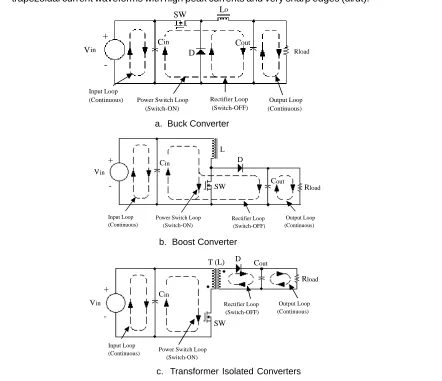
Switching power supplies have large current pulses with very sharp edges flowing within the power supply circuit. These large current pulses have the greatest effect on the creation of EMI, and should be the primary focus of the PCB designer. These currents flow in definable “loops” and the circuits carrying these currents should be laid-out first. The low-level control circuitry is then subsequently coupled into specific spots in the layout. These loops are diagrammed in figure 1 for the three major basic topologies of switching power supplies. All of the other topologies are varia-tions of these three.
The loops shown in figure 1 can be listed in the order of their greatest affect on noise generation and operational performance:
1. The power switch high current loop. 2. The rectifier high current loop. 3. The input source loop. 4. The output load loop.
+The input source and output load current loops are filtered by input and output EMI filters (not shown). Their currents are composed of largely DC current. The AC components of these currents are created by the power supply and should be kept to a minimum. These AC components are the elements that make-up conducted EMI. Any AC energy that is allowed to pass over a long enough length of a conductor, is radiated into the product’s environment.
The input and output loops are of secondary concern because the large AC pulses seen inside the supply are filtered by the input filter and output filter capacitors respectively. This makes their potential for creating high frequency noise problems less than the two AC loops. These loops should be analyzed later since they are directly measured by the regulatory agencies. The power switch and rectifier current loops are entirely AC, or more appropriately, pulsating DC. They have trapezoidal current waveforms with high peak currents and very sharp edges (di/dt).
b. Boost Converter a. Buck Converter
Rload
Power Switch Loop (Switch-ON)
Rectifier Loop (Switch-OFF) Input Loop
(Continuous) Output Loop (Continuous)
Vin
SW
D Lo
Cin Cout
- +
Rectifier Loop (Switch-OFF) Power Switch Loop
(Switch-ON) Input Loop (Continuous) Output Loop (Continuous) D L SW Vin + - Cin Cout Rload ( ) Input Loop
(Continuous) Power Switch Loop
Rectifier Loop (Switch-OFF)
Output Loop (Continuous)
SW
D Cout
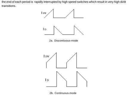
[image:2.612.85.527.316.697.2]Some representative waveforms can be seen in figure 2. PWM switching power supplies operate in one of these two modes: the discontinuous-mode, as seen in figure 2A, and the continuous-mode as seen in figure 2B. The discontinuous-mode is when the output rectifier(s) is allowed to com-pletely empty the magnetic element of its magnetic energy before the power switch once again turns-on. The continuous-mode is when some residual energy is allowed to remain in the mag-neticelement when the power switch begins to turn-on for the next cycle. The current flowing at the end of each period is rapidly interrupted by high speed switches which result in very high di/dt transitions.
2a. Discontiuous-mode
[image:3.612.91.527.164.498.2]2b. Continuous-mode
Figure 2. The Modes of Operation of Switching Power Supplies
ISW
ID
I
SWI
DThe power switch loop and the output rectifier loop(s) should be laid out so that the “loop” has a very small circumference and is composed of traces that are short in length and wide in width. First, the circumference of the loop controls the amount of RF energy that can be radiated at lower frequencies where a significant amount of conducted RF energy exists. By making the loop cir-cumference as short as possible, one does not provide an efficient antenna for these lower noise frequencies. A typical power supply conducts noise frequency components that remain very high until about 100 times the switching frequency and then fall at a rate of between -20 to -40 dB per decade. The lower the frequency a loop is allowed to radiate, the more energy is allowed to escape into the environment. Secondly, the width of the traces used within the high current loops directly dictate the amount of voltage drop which will appear around the loop. This voltage drop, when created by high current, also creates RF radiation. The inductance and resistance exhibited by a trace is inversely proportional to its width. Inductance lowers the frequency response of a loop and therefore is a more efficient antenna at lower frequencies. So the loop traces should be as wide as possible. Wide traces also provide better heatsinking for the power switch and rectifier(s). An example of a layout for the power switch and rectifier loops in a buck converter is shown in figure 3. Notice the very short distances between all members of the two main AC loops.
Figure 3. Example layout for a Buck Converter Power Stage Schematic.
Vin Cin Cout Vout
inductor Power Switch
To
Control Diode
inductor Power Switch
Gate
Vin
Cin
Cout
Diode
Vout
Control Connection
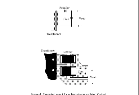
The output rectifier loop in transformer-isolated topologies have the same layout requirements as the input power switch loop. An example layout for the rectifier loop within a flyback converter can be seen in figure 4.
Figure 4. Example Layout for a Transformer-isolated Output Transformer
Rectifier
Vout Cout
Vout Cout
Rectifier Transformer
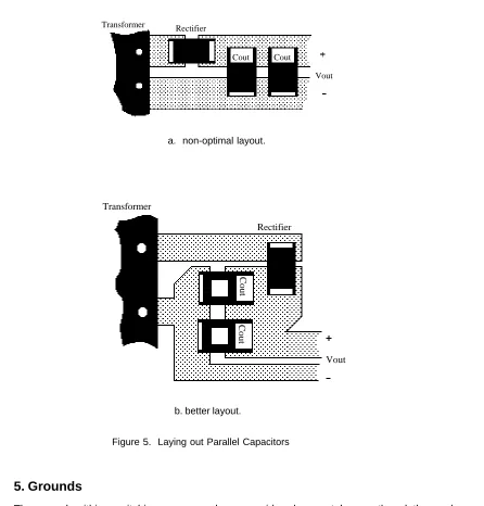
4. Paralleled Capacitors.
a. non-optimal layout.
[image:6.612.84.530.81.547.2]b. better layout.
Figure 5. Laying out Parallel Capacitors
5. Grounds
The grounds within a switching power supply are considered separately, even though they make-up one leg of the high current loops previously discussed. They are special in that they represent the lowest potential return path for the currents and the potential from which all other signals are measured. They have both DC and AC signals being conducted between various points in the physical ground system. There are sections of the ground system that should be considered separately from one another. If these grounds are interconnected improperly, the power supply can become unstable.
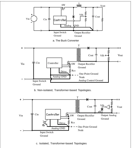
There are three grounds within a switching power supply: 1. the input high-current ground, 2. the output high-current ground and 3. the low-level control ground. The grounds for the three major switching power supply topologies are shown in figure 6.
Vout Cout
Cout Rectifier
Transformer
Transformer
Rectifier
Vout
Cout
Figure 6. Ground Arrangements for various Topologies c. Isolated, Transformer-based Topologies
a. The Buck Converter
b. Non-isolated, Transformer-based Topologies.
As one may notice from the diagrams in figure 6, the connection of the low-level control ground to the overall grounding system is very specific. The first factor to understand is that the power supply controller’s main purpose is to precisely regulate the output voltage. To do this, the high-gain error amplifier should be directly connected to the bottom of the output filter capacitor. In this way, noise voltages from the high current loops are not summed into the low-level sense signals. Secondly, the controller usually needs to sense a small signal across a current sensing resistor as well as drive the gate or base of a power switch.
Vin
Vout
Analog GND
Output Rectifier Ground
Input Switch Ground
Analog Control Ground Drive
Cout
Cin Controller
T
Vfb
One-Point Ground Node
SW
Rcs
Output Analog Ground
Vout
Vin Output Rectifier
Ground
One-Point Ground Node
Analog GND
Input Switch Ground
Drive
Cout Vfb
Cin
T
Rcs SW
Cout Vfb
SW
Cin Vin
Input Switch Ground
Output Rectifier Ground Analog GND
If there are separate analog and power ground pins on the controller IC, they should be routed separately to the ground side of the current sensing resistor. If the IC does not have separate ground pins, then the trace between the IC and the ground end of the current sense resistor should be short and wide.
Another good practice to reduce radiated EMI is to place large areas of ground plane on the opposite side of the PCB and around these high current traces. The ground planes act as electro-static shields for some of the RF energy already radiated. These large conductor areas trap radiated EMI and dissipate them within eddy currents created by the RF energy.
One last and very important factor in designing PCB layouts for switching power supplies is the capacitive coupling of the AC node voltages into their heatsinks or into nearby ground planes. The problem is very severe in through-hole designs, but can also be a problem in surface-mount applications.
The problem is created by the high AC voltages that appear on specific nodes within the switching power supply. Examples of these nodes are the drain connection of the power switch, the AC node connected to an output rectifier, and any snubber or clamp networks connected to these nodes.
In through-hole applications, the power switch is typically a power package with a tab which is bolted to a heatsink with a 5 mil (0.005 inch, 0.13 mm) insulator between them. The drain tab of the power switch has AC peak-to-peak voltages of either one or two times the input voltage. In many supplies, the heatsink is earth grounded which provides a path for the capacitively coupled noise energy to exit the enclosure. Insulator makers have pads that have embedded foil which cuts the capacitance in half.
The problem is less significant in surface-mount applications since the capacitance formed by 0.062 inch (1.6 mm) thick F4 material is much smaller. Additionally, it is rare that earth ground is brought onto the PCB, but the noise could couple into other sensitive signals. The goal is to reduce this parasitic capacitance by creating PCB structures that exhibit low capacitance, such as locating susceptable signals one the same side instead of underneath the noisy node or cross-hatching any ground planes beneath the noisy node.
7. The EMI Filter Layout
Now is the appropriate time to consider the layout of the EMI filter. An EMI filter is needed anytime a power lead or leads are allowed to exit the product’s enclosure, which hopefully also provides some RF shielding. These filters are intended to reduce, but cannot completely eliminate, the high frequency currents conducted within the DC input and/or output wiring. Conducted EMI is tested by the regulatory bodies by placing a special cur-rent transformer (a line impedance stabi-lization network (LISN)) in series with the input and/or output power lines. The tester then plots the spectrum of the emerging current waveform from DC to over 1 GHz. The product under test must emit a current spectrum lower than the specified limits at all frequencies.
The filters are designed to not pass the high frequency noise created by the PWM switching power supply. If the parasitic factors of the filter components themselves are not well known and the components are not laid-out properly, some switching energy can couple around the filter compo-nents to traces on the other side of the filter. This allows some of the high frequency energy to escape into the environment or into the rest of the system. Once in the external wiring, this conducted RF energy will then radiate into the surrounding environment as radiated EMI.
Example Printed Circuit Board Designs
The design examples are those of DC/DC power supplies which are usually part of a larger printed circuit board. They generally are powered from an external AC/DC power supply. Therefore the following examples are designed as layouts, that are part of a larger PCB not bounded by edges of a PCB.
The primary focus of the following PCB examples is that of the physical PCB design. The ex-amples have not been built and debugged. Sub-circuits such as snubbers and clamps may need to be added to make the designs practical.
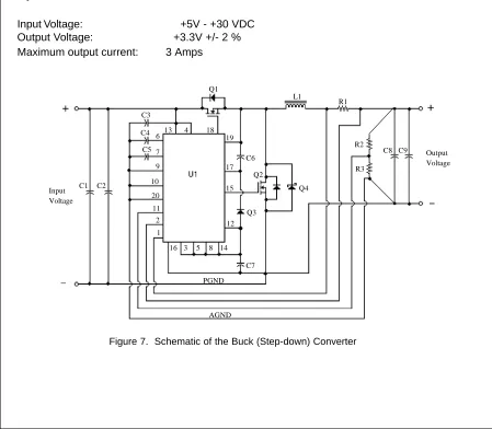
The buck (step-down) converter:
This design example would provide an output voltage of 3.3 VDC and can deliver up to 3 Amps to a load. It is powered from a 12 volt battery pack or from a wall transformer. The input voltage may go as high as 30 VDC which makes it applicable for many portable applications such as notebook computers. This circuit may be easily“scaled” to operate at different input voltages or to deliver a different output voltage or maximum current. The semiconductors, filter capacitors, the inductor, and obviously the PCB layout would have to be modified to operate optimally for any new require-ments.
Specifications
[image:9.612.81.530.328.720.2]Input Voltage: +5V - +30 VDC Output Voltage: +3.3V +/- 2 % Maximum output current: 3 Amps
Parts List for the Buck Converter in Figure 7:
Designation Mfr Part No. Value Rating Package
C1 Sprague 593D226X0035E2W 22uF 35V E-case
C2 Sprague 593D226X0035E2W 22uF 35V E-case
C3 Mepco C105M1206ZFLB 0.1uF 50V 1206
C4 Mepco C102M0805ZFLB 1nF 50V 805
C5 Sprague 293D155X0010A2T 1.5uF 10V A-case
C6 Mepco C102M0805ZFLB 1nF 50V 805
C7 Sprague 293D475X0010B2T 4.7uF 10V B-case
C8 Sprague 594D227X0010D2T 220uF 10V D-case
C9 Sprague 594D227X0010D2T 220uF 10V D-case
L1 Coilcraft DO3316-103 10uH 3.8A Custom
Q1 Fairchild FDS4410 - 10A,30V SO8
Q2 Fairchild FDS4410 - 10A,30V SO8
Q3 Fairchild MMBD914 - 0.1A,100V SOT23
Q4 Fairchild MBRS130L - 1A, 30V SMC
R1 Dale WSL-2010-R020F 20mý 1% 2010
R2 Dale CRCW08052211FB02 2.11K 1% 805
R3 Dale CRCW08051101FB02 1.10K 1% 805
Figure 8. PCB Layout for the Buck Converter
The boost converter
This design example derives its input power from a +5V logic supply and could provide power to any associated analog functions or interface circuits. Once again, the design can be scaled.
Specifications
Figure 9. Boost (Step-up) Converter
Parts List:
Designation Mfr Part No. Value Rating Package
C1 Sprague 293D107X0010D2T 100uF 10V D-case
C2 Mepco C105M1206ZFLB 0.1uF 50V 1206
C3 Mepco C105M1206ZFLB 0.1uF 50V 120
C4 Mepco C101M0805ZFLB 100pF 50V 805
C5 Sprague 293D686X0016D2T 68uF 16V D-case
C6 Sprague 293D686X0016D2T 68uF 16V D-case
C7 Sprague 293D686X0016D2T 68uF 16V D-case
L1 Coilcraft DO3316-223 22uH 2.6A Custom
Q1 Fairchild FDS6612 - 8.4A,30V SO8
Q2 Fairchild MBRS130L - 1A, 30V SMB
R1 Dale WSL-2010-R040F 40mý 1% 2010
R2 Dale CRCW08051273FB02 127K 1% 805
R3 Dale CRCW08051822FB02 18.2K 1% 805
U1 MAXIM MAX1771 - 17V(max) SO8
C1 C2
C3
C4
C5 R1
R2
R3 Q1
Q2 L1
U1 MAX1771 FB
AGND
SHDN REF
GND CS EXT V+
Input Voltage
The flyback converter
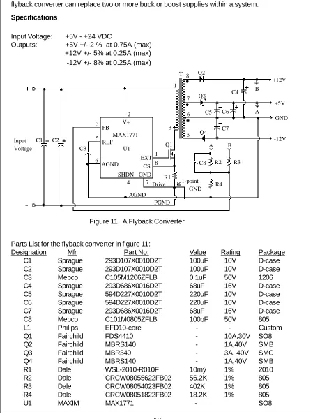
This flyback converter can be used as a step-up, step-down and/or an inverting power supply. Its transformer is more complicated to design, but its added cost can be recovered considering the flyback converter can replace two or more buck or boost supplies within a system.
Parts List for the flyback converter in figure 11:
Designation Mfr Part No: Value Rating Package
C1 Sprague 293D107X0010D2T 100uF 10V D-case
C2 Sprague 293D107X0010D2T 100uF 10V D-case
C3 Mepco C105M1206ZFLB 0.1uF 50V 1206
C4 Sprague 293D686X0016D2T 68uF 16V D-case
C5 Sprague 594D227X0010D2T 220uF 10V D-case
C6 Sprague 594D227X0010D2T 220uF 10V D-case
C7 Sprague 293D686X0016D2T 68uF 16V D-case
C8 Mepco C101M0805ZFLB 100pF 50V 805
L1 Philips EFD10-core - - Custom
Q1 Fairchild FDS4410 - 10A,30V SO8
Q2 Fairchild MBRS140 - 1A,40V SMB
Q3 Fairchild MBR340 - 3A, 40V SMC
Q4 Fairchild MBRS140 - 1A,40V SMB
R1 Dale WSL-2010-R010F 10mý 1% 2010
R2 Dale CRCW08055622FB02 56.2K 1% 805
R3 Dale CRCW08054023FB02 402K 1% 805
[image:13.612.81.530.128.728.2]MAX1771 U1 FB REF AGND SHDN GND CS EXT V+ 1 2 3 4 5 6 7 8 Input Voltage C1 C2 C3 C4 C5 C6 C7 Q1 Q2 Q3 Q4 1 3 5 6 7 8 T +12V +5V GND -12V A B A B C8 R1 R2 R3 R4 1-point GND AGND PGND Drive
Figure 11. A Flyback Converter Specifications
Input Voltage: +5V - +24 VDC
Figure 12. PCB Layout for a flyback converter
1. Brown, Marty, Power Supply Cookbook, Butterworth-Heinemann, 1994, pp 89-94, 224, 216-225.
2. Brown, Marty, Practical Switching Power Suppy Design, Academic Press, Inc., 1990, pp 115-119, 125-128.
3. Linear Technology, Linear View v2.0, CD, Linear Technology Corp. 1997.
TRADEMARKS
ACEx™ CoolFET™ CROSSVOLT™ E2CMOSTM FACT™
FACT Quiet Series™ FAST®
FASTr™ GTO™ HiSeC™
The following are registered and unregistered trademarks Fairchild Semiconductor owns or is authorized to use and is not intended to be an exhaustive list of all such trademarks.
LIFE SUPPORT POLICY
FAIRCHILD’S PRODUCTS ARE NOT AUTHORIZED FOR USE AS CRITICAL COMPONENTS IN LIFE SUPPORT DEVICES OR SYSTEMS WITHOUT THE EXPRESS WRITTEN APPROVAL OF FAIRCHILD SEMICONDUCTOR CORPORATION. As used herein:
ISOPLANAR™ MICROWIRE™ POP™ PowerTrench™ QS™ Quiet Series™ SuperSOT™-3 SuperSOT™-6 SuperSOT™-8 TinyLogic™
1. Life support devices or systems are devices or systems which, (a) are intended for surgical implant into the body, or (b) support or sustain life, or (c) whose failure to perform when properly used in accordance with instructions for use provided in the labeling, can be reasonably expected to result in significant injury to the user.
2. A critical component is any component of a life support device or system whose failure to perform can be reasonably expected to cause the failure of the life support device or system, or to affect its safety or effectiveness.
PRODUCT STATUS DEFINITIONS
Definition of Terms
Datasheet Identification Product Status Definition
Advance Information
Preliminary
No Identification Needed
Obsolete
This datasheet contains the design specifications for product development. Specifications may change in any manner without notice.
This datasheet contains preliminary data, and supplementary data will be published at a later date. Fairchild Semiconductor reserves the right to make changes at any time without notice in order to improve design.
This datasheet contains final specifications. Fairchild Semiconductor reserves the right to make changes at any time without notice in order to improve design.
This datasheet contains specifications on a product that has been discontinued by Fairchild semiconductor. The datasheet is printed for reference information only. Formative or
In Design
First Production
Full Production
Not In Production
DISCLAIMER
FAIRCHILD SEMICONDUCTOR RESERVES THE RIGHT TO MAKE CHANGES WITHOUT FURTHER NOTICE TO ANY PRODUCTS HEREIN TO IMPROVE RELIABILITY, FUNCTION OR DESIGN. FAIRCHILD DOES NOT ASSUME ANY LIABILITY ARISING OUT OF THE APPLICATION OR USE OF ANY PRODUCT OR CIRCUIT DESCRIBED HEREIN; NEITHER DOES IT CONVEY ANY LICENSE UNDER ITS PATENT RIGHTS, NOR THE RIGHTS OF OTHERS.