LASER-INDUCED CRYSTALLIZATION OF SPUTTERED UNHYDROGENATED SILICON AT LOW TEMPERATURES
E. Saugar1, J.P. González1, S. Fernández1, J.J. Gandía1, J. Cárabe1, D. Canteli2, M. Morales2, C. Molpeceres2, F. García-Pérez3, M.B. Gómez-Mancebo3.
1
Energy Department, CIEMAT, Madrid, 28040, Spain 2
Centro Láser, Universidad Politécnica de Madrid, Madrid, 28038, Spain 3
Chemistry Division, CIEMAT, Madrid, 28040, Spain
ABSTRACT: 10-µm-thick non-hydrogenated amorphous-silicon (a-Si) films were deposited at relatively high rates (≥ 10 Å/s) by radio-frequency magnetron sputtering (RFMS) on different large-area buffer-layer-coated glass substrates at deposition temperatures ranging from room temperature (RT) to 300ºC. These amorphous samples were subsequently crystallized by means of a continuous-wave diode laser, looking for conditions to reach liquid-phase crystallization. The influence of deposition conditions on the quality of the final micro-crystalline silicon films has been studied.
Keywords: amorphous silicon, liquid-phase crystallization, multicrystalline silicon
1 INTRODUCTION
The current photovoltaic scenario is dominated by wafer-based silicon technology, which has led the worldwide market for a long time owing to its good performance-to-cost ratio [1]. Nevertheless, and in spite of the dramatic cost reduction undergone by mono- and multicrystalline silicon wafers in the last decade, the further gain in competitiveness of photovoltaic devices requires intensive search for new approaches in what concerns semiconductor devices [2]. The road to find new solutions and new forms of silicon go through thickness reduction, kerf avoidance and manufacturing-cost lowering. From this point of view, liquid-phase crystallization (LPC) has arisen as a promising and novel method [3] above solid-phase crystallization (SPC), for which a higher thermal budget is needed. Furthermore, cells made from SPC silicon exhibit lower open-circuit voltages [4].
Previous works have demonstrated satisfactory LPC-silicon results in terms of material grain sizes and cell open-circuit voltages well above 600 mV [5]. While it is true that those results are promising, the substrate temperatures involved exceed 600ºC, thus limiting the attractiveness of the process[6].
In this work the quality of polycrystalline silicon (poly-Si) obtained from a-Si deposited at relatively low temperatures (300ºC) is analyzed in what concerns crystalline fraction and grain size. The effects of deposition conditions, buffer layer, grain size and crystal preferential orientation are discussed.
2 EXPERIMENTAL
10-µm-thick non-hydrogenated a-Si films were deposited onto Corning Eagle XG® glass substrates coated with a 200-nm SiO2 layer by using an RFMS system. Prior to the deposition, the substrates were cleaned in an ultrasonic bath, subsequently rinsed in ethanol and dried with nitrogen. Two series were deposited respectively at room temperature and 300ºC, under a working pressure of 1.07 Pa. The measurement of substrate temperature was performed by means of a type-K reference thermocouple.
The a-Si was treated with a continuous-wave diode laser emitting at 940 nm and forming a spot which is linear along the X axis and Gaussian in the Y axis, and whose dimensions in focus are 16.5 mm × 2.16 mm. During the crystallization process, in order to reduce
thermal stress and prevent cracks, the samples were subjected to high temperatures (650ºC) for a short time. The samples were moved in a straight line using a constant scanning speed ranging from 400 mm/min to 1000 mm/min and irradiance from 900 J/cm2·s to 1650 J/cm2·s. Each sample was crystallized in distinct zones at different laser conditions.
The quality of the micro-crystalline silicon obtained has been evaluated by X-Ray diffraction (XRD) using a PANalytical X’pert Pro diffractometer operating in θ – θ configuration, with CuKα radiation (45kV – 40 mA), in the angular range 20º < 2θ < 80º. Phase identification was obtained by comparison to the Inorganic Crystal Structure Database (ICDS). In order to study the material modifications caused during the laser process, Raman spectra were measured by using a commercial InVia Renishaw Raman spectrometer employing the 514.5-nm line of an Ar laser.
3 RESULTS AND DISCUSSION
3.1 Buffer layer and stability
As known from literature [7], diffusion barriers play an important role in the laser crystallization process. On the one hand, they are necessary in order to avoid contamination of the silicon due to diffusion of species from the glass substrate [8]. On the other hand, they prevent the formation of droplets due to surface tension during liquid-phase crystallization [3][8]. With this in mind, we have mutually compared the behavior of different samples on glass substrates with and without a 200-nm SiO2 coating during the laser process.
Table 1: Process conditions and results obtained for two samples deposited at room temperature. A1 on bare glass and B1 on 200-nm SiO2-coated glass.
ID Zone Irradiance (J/cm2·s)
Scan speed (mm/min)
Status
A1 1 1164 ± 49 600 Damaged B1 1 1164 ± 49 600 Crystallized
3.2 Structural properties
Once the need for diffusion barriers had been established, the influence of substrate temperature on the crystallization process was investigated. Although very high deposition temperatures, such as those previously cited [6] (about 600 ºC) were avoided, samples C1 and D1 were respectively deposited by sputtering at 300 ºC and room temperature (RT). Different regions of these samples were subsequently laser-processed in different conditions (see please Table 2).
Figure 1a and 1b show the corresponding Raman spectra of the samples, including a <100> monocrystalline-silicon wafer for reference. The Raman spectra were deconvoluted into three Gaussian peaks respectively at 480 cm-1 (corresponding to the amorphous-silicon phase), 510 cm-1 (corresponding to a defective crystalline phase) [9] and at 520 cm-1 (corresponding to silicon crystallites). From the integration of the deconvoluted Gaussian peaks it is possible to calculate the crystalline fraction (ΧC) through the following equation:
𝑋𝐶=
(𝐼
520+ 𝐼510)
(𝐼
520+ 𝐼510+ 𝐼480)
(a)
(b)
Figure 1: Raman spectra of 10-µm-thick magnetron-sputtered silicon films deposited at different temperatures: sample C1 at 300ºC (a) and D1 at room temperature (RT) (b). The spectrum of a c-Si reference has been added. The graph inset shows a detail of the peak region.
As it can be observed on Figure 1, the spectrum of the c-Si reference (green curves) has its peak at 520 cm-1 with a full-width half maximum (FWHM) of 4.5 cm-1 approximately. However, the peaks of samples deposited
at respectively 300ºC and room temperature differ both mutually and with respect to the c-Si reference peak both in position and in FWHM. Furthermore, for sample D1, a slight contribution due to the amorphous phase present in the material can be observed at 490 cm-1.
The sample deposited at relatively high temperature (C1) allows higher irradiances and this means higher crystalline fraction values of up to 20% more than the sample deposited at room temperature.
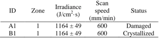
These samples have also been evaluated concerning their crystal orientation and grain size from X-Ray diffraction (XRD). Figure 2 shows the respective XRD patterns of samples C1 (a) and D1 (b).
(a)
(b)
Figure 2: X-Ray diffraction patterns (XRD) of respectively sample C1, deposited at 300ºC (Figure 2a) and sample D1, deposited at RT (Figure 2b). The different patterns in each plot correspond to different zones over the samples.
The XRD results evidence that laser-induced crystallization generates different crystal orientations in different zones, i.e. for different laser irradiances. However, by comparing the relative intensities of the XRD patterns it becomes easy to notice that <111> is the main orientation in both samples. Table 2 shows the crystalline fraction of each zone and the respective grain size as obtained from the Scherrer equation [10].
Table 2: Crystalline fraction derived from the integration of deconvoluted Raman peaks, and grain size obtained from XRD pattern by using Scherrer equation, of two samples deposited respectively at 300ºC (C1) and RT (D1).
ID Zone Irradiance / Scan speed XC
Grain Size (nm)
C1
1 1384 ± 51 W cm -2
1000 mm min-1 91 ± 3 70 ± 2
2 1538 ± 52 W cm -2
1000 mm min-1 93 ± 3 134 ± 5
3 1630 ± 53 W cm -2
1000 mm min-1 96 ± 3 2450 ± 400
D1
1 914 ± 47 W cm -2
400 mm min-1 84 ± 3 50 ± 1
2 963 ± 48 W cm -2
400 mm min-1 81 ± 2 57 ± 1
3 1164 ± 49 W cm -2
600 mm min-1 75 ± 1 57 ± 1
4 1222 ± 50 W cm -2
600 mm min-1 85 ± 3 71 ± 2
(a)
Figure 3: Grain size in logarithmic scale versus irradiance.
In order to further investigate how substrate temperature affects the samples and their compactness, the refractive index of different samples deposited at different substrate temperatures has been studied. It is well known that refractive index is an important optical parameter related to mass- and void density [11]. From the Clausius-Mossoti equation, mass density can be drawn [12].
𝜌𝑎−𝑆𝑖= (
𝑛∞2 − 1
𝑛∞2 + 2)
3𝑚𝑆𝑖
8𝜋𝛼𝑆𝑖−𝑆𝑖
where 𝑚𝑆𝑖 is the mass of the silicon atom, n∞ is the refractive index at long wavelengths and 𝛼𝑆𝑖−𝑆𝑖 is the bond polarizability in the amorphous phase. The value
𝛼𝑆𝑖−𝑆𝑖= 1.96 × 10⁻²⁴ cm3 is taken from [12].
Four a-Si samples have been deposited in the same conditions as for C1 and D1 except for substrate temperature, which has been varied between RT and 300ºC.
Figure 4 shows the refractive indexes of four samples deposited at 1.07 Pa at different temperatures ranging from RT to 300ºC. In the whole range covered an abrupt
refractive-index growth with increasing substrate temperature is appreciated. This result is attributed to a reduction of void density [13].
From the analysis of refractive-index dispersion by means of the Wemple-DiDomenico dispersion model [14], below the interband absorption edge it is possible to obtain important information about atomic structure and mass density. The refractive index values were fitted to the WDD dispersion model according the following equation:
𝑛(𝐸)2− 1 = 𝐸𝑑𝐸0
(𝐸𝑑2− 𝐸2)
Figure 4: Refractive indexes of four a-Si samples deposited at different substrate temperatures. The circle inset illustrates the refractive-index rise with temperature.
Ed is an important parameter, which is closely related to the structural characteristics of the material and obeys the following relationship:
𝐸𝑑= 𝛽𝑁𝑐𝑍𝑎𝑁𝑒,
where NC is the coordination number of the cation nearest
neighbor to the anion, and Za, Ne, β are constants [14]. The voids and the low packing of the amorphous lattice result in low density and coordination-number values [12]. In this sense, the estimate of the coordination number can provide information about the evolution of void density with substrate temperature. According to Wemple [15], the following expression allows us calculate the coordination number:
𝐸𝑑𝑎
𝐸𝑑𝑥= (
𝜌𝑎
𝜌𝑥) (
𝑁𝑐𝑎
𝑁𝑐𝑥)
where ρ is the density, x and a refer to crystalline- and amorphous phases respectively.
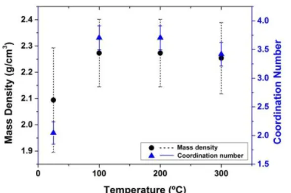
Figure 5: Mass density (black dots with short dash error bars) and coordination number Nc (blue triangles with solid error bars) versus substrate temperature.
The mass-density values obtained increase from 2.1 g/cm3 for sample deposited at RT to 2.3 g/cm3 for sample deposited at 300ºC, whereas the coordination number stretches from 2.1 to 3.7 in the same substrate-temperature range. The typical values, according to bibliography [12][16], are ρ = 2.33 g/cm3 and Nc = 4 for
c-Si, ρ = 2.29 g/cm3 and Nc = 3.7 for a-Si.
In view of the results obtained, the samples deposited at moderately high deposition temperatures show higher compactness than those deposited at RT. Such a result is consistent with the finding that high crystalline fractions and grain sizes of the order of microns are only obtained from amorphous-silicon samples deposited at moderately high temperatures (of the order of 300 ºC, yet well below the high temperatures largely found in the literature). The emergence of this microcrystalline material is attributed to the achievement of liquid-phase crystallisation in the conditions indicated.
4 CONCLUSIONS
In this work several samples have been deposited onto different substrates, either bare or coated with a 200-nm SiO2 layer, with different substrate temperatures. Firstly, it has been noted that the buffer layer plays a fundamental role to obtain a successful crystallization process by improving wettability and enhancing thermal stability under high laser irradiances.
Secondly, the relevance of substrate deposition temperature has been assessed. It has been observed that the samples deposited at moderately high (although much lower than those typically found in the literature) substrate temperatures show higher compactness and mass density than those deposited at RT. The effect is attributed to the activation of different diffusion processes during deposition, leading to the rearrangement of silicon atoms. Furthermore, these samples offer better performance under high irradiances, resulting in increased crystalline fractions and grain sizes. The results, in summary, suggest that the samples having micron-size crystallites are those for which process conditions trigger liquid-phase crystallization. Such an achievement in spite of the moderate substrate temperatures (not higher than 300ºC) is considered quite relevant.
5 ACKNOWLEDGEMENTS
This research has been partially supported by the Spanish Research Agency (AEI) and Ministry of Economy,
Industry and competitiveness through project CHENOC (ENE2016-78933-C4).
6 REFERENCES
[1] International Technology Roadmap for Photovoltaics (ITRPV) Results 2015 (2016) by SEMI PV Group.
[2] G. Bye and B. Ceccaroli, “Solar grade silicon: Technology status and industrial trends,” Sol. Energy Mater. Sol. Cells, vol. 130, pp. 634–646, Nov. 2014.
[3] J. Haschke, D. Amkreutz, and B. Rech, “Liquid phase crystallized silicon on glass: Technology, material quality and back contacted heterojunction solar cells,” Jpn. J. Appl. Phys., vol. 55, no. 4S, p. 04EA04, Apr. 2016.
[4] S. Gall and B. Rech, “Technological status of polycrystalline silicon thin-film solar cells on glass,” Sol. Energy Mater. Sol. Cells, vol. 119, pp. 306–308, Dec. 2013.
[5] J. Haschke, D. Amkreutz, L. Korte, F. Ruske, and B. Rech, “Towards wafer quality crystalline silicon thin-film solar cells on glass,” Sol. Energy Mater. Sol. Cells, vol. 128, pp. 190–197, 2014.
[6] D. Amkreutz, J. Haschke, T. Häring, F. Ruske, and B. Rech, “Conversion efficiency and process stability improvement of electron beam crystallized thin film silicon solar cells on glass,” Sol. Energy Mater. Sol. Cells, vol. 123, pp. 13–16, 2014.
[7] D. Amkreutz, J. Müller, M. Schmidt, T. Hänel, and T. F. Schulze, “Electron-beam crystallized large grained silicon solar cell on glass substrate,” Prog. Photovoltaics Res. Appl., vol. 19, no. 8, pp. 937–945, Dec. 2011.
[8] J. Dore, S. Varlamov, and M. A. Green, “Intermediate Layer Development for Laser-Crystallized Thin-Film Silicon Solar Cells on Glass,” IEEE J. Photovoltaics, vol. 5, no. 1, pp. 9–16, Jan. 2015.
[9] C. Droz, “Thin Film Microcrystalline Silicon Layers and Solar Cells : Microstructure and Electrical Performances,” Ph.D. dissertation Université de Neuchâtel, Neuchâtel, 2003. [10] A. L. Patterson, “The Scherrer formula for
X-Ray particle size determination,” Phys. Rev., vol. 56, pp. 978–982, 1939.
[11] J. Müllerová, L. Prusáková, M. Netrvalová, V. Vavrunková, and P. Sutta, “A study of optical absorption in amorphous hydrogenated silicon thin films of varied thickness,” Appl. Surf. Sci., vol. 256, no. 18, pp. 5667–5671, 2010.
[12] A. H. M. Smets, W. M. M. Kessels, and M. C. M. Van de Sanden, “Vacancies and voids in hydrogenated amorphous silicon,” Appl. Phys. Lett., vol. 82, no. 10, pp. 1547–1549, 2003. [13] H. Chen and W. Z. Shen, “Perspectives in the
characteristics and applications of Tauc-Lorentz dielectric function model,” Eur. Phys. J. B, vol. 43 (4), pp. 503–507, 2005.
[14] S. H. Wemple and M. DiDomenico, “Behavior of the electronic dielectric constant in covalent and ionic materials,” Phys. Rev. B, vol. 3, no. 4, pp. 1338–1351, 1971.
Amorphous Semiconductors and Glasses,” Phys. Rev. B, vol. 7, no. 8, pp. 3767–3777, 1973. [16] K. Laaziri, S. Kycia, S. Roorda, M. Chicoine, J.