transport properties of silicon quantum dots for
optoelectronic applications
Núria García Castelló
Aquesta tesi doctoral està subjecta a la llicència Reconeixement 3.0. Espanya de Creative
Commons.
Esta tesis doctoral está sujeta a la licencia Reconocimiento 3.0. España de Creative
Commons.
Departament d’Electr`onica
MEM `ORIA DE TESI DOCTORAL PRESENTADA PER OPTAR AL T´ITOL DE DOCTORA EN NANOCI`ENCIES
PER LA UNIVERSITAT DE BARCELONA
Atomistic study of structural and
electronic transport properties of
silicon quantum dots for
optoelectronic applications
N´uria Garc´ıa Castell´o
Directors: Dr. Albert Cirera Hern´
andez
Dr. Juan Daniel Prades Garc´ıa
Tutor: Dr. Albert Cirera Hern´andez
Programa de Doctorat en Nanoci`encies
Atomistic study of structural and electronic
transport properties of silicon quantum dots
for optoelectronic applications
Tesi que presenta
N´
uria Garc´ıa Castell´
o
per optar al t´ıtol de Doctora per la Universitat de Barcelona
Directors de Tesi:
Dr. Albert Cirera Hern´andez Dr. Juan Daniel Prades Garc´ıa
Departament d’Electr`onica
Grup de Micro-Nanotecnologies i Nanosc`opies per Dispositius Electr`onics i Fot`onics (MIND)
Acknowledgement
I would like to acknowledge my supervisors, Albert and Dani, for their patience and guidance,
Sergio and Roberto for the important work that they have done,
Stefano and the Modena group, specially Feffe and Ivan, for their hospitality,
the colleagues of the office and mindundis (Giovanni, Oriol, Luis, Xavi, Bea, Jordi, A¨ıda, Olga, Sergi, Elena, Lloren¸c, Radouane, Roman, Juli`a, Oriol, Alberto, JM and JM, Yonder, els Lluisos) for the coffee breaks and Friday out-lunch time and evening games (and beers and wine and ... well ... other drinks hidden in that place),
my group of theorists (Blai and Blai, Adriana, Ivan, Marina, Carmen, Gen´ıs, Miquel, Markus, Renau, Luis, Dani, Axel, Blanca, and also Gerard and Louis) for lunch time, and coffee time, and piti time, and whatever
time,
my friends in Modena (Miquel and Oliver and the others of thehispanic
community in the faculty, D´aire and Erik and the other Ferrari guys, Sara and the Couchsurfing family) for all the good times together and specially for their capacity to do something any time I was bored,
my friends of all times (Carla, Joan, Arnau, Lau, Pau, Uri, Adri`a, Nesi, Eli, Marina, Jaume, Clara, Irene, Jordi, Merc`e, Uri) for the weekly bar time,
and my family for their unconditional support.
And a special thanks to my life comrade during these years, M`axim. Also to jazz music and my friends, Juanan and Lucas, that tried to play with me when my head was thinking in all this stuff.
Contents
1 Preface 1
1.1 Transport in nanoelectronics . . . 3
1.2 Brief overview . . . 6
1.3 Aim of this PhD Thesis . . . 9
1.4 Outline . . . 9
2 Theoretical framework 13 2.1 Density Functional Theory . . . 13
2.1.1 Some words about Hartree-Fock, correlation and ex-change . . . 14
2.1.2 About Density Functional Theory . . . 16
2.1.3 Approximations in present DFT computations and notes about the code . . . 22
2.2 Non-Equilibrium Green Functions Formalism . . . 27
2.2.1 Description of nanodevices inside NEGFF . . . 27
2.2.2 Expressions used in TranSIESTA code . . . 29
2.2.3 Exemple of the use of NEGFF in a transport calculation 34 2.3 Transfer Hamiltonian formalism . . . 36
2.3.1 Transfer Hamiltonian formalism: transport in quan-tum devices . . . 36
2.3.2 WKB approximation: expressions for transmission co-efficients . . . 38
2.3.3 Brief overview about SIMQdot, the code used in trans-port calculations . . . 39
3 Transport of bulk Si in the main crystallographic growth directions of Si nanowires 43 3.1 Computational details . . . 46
3.2 Thermodynamic model for the stability of polymorphs in Si NWs . . . 47
3.3 Electronic transport in bulk Si . . . 53
3.3.1 Atomistic models of the main growth directions of Si NWs . . . 53
3.3.2 Si bulk transport properties . . . 55
3.4 Conclusions . . . 61
3.4.1 Thermodynamic model for the stability of polymorphs in Si NWs . . . 62
3.4.2 Electronic transport in bulk Si . . . 62
3.4.3 DFT-NEGFF methodology to study transport in nanos-tructures . . . 63
4 Silicon quantum dots embedded in a SiO2 matrix 65 4.1 Computational details . . . 66
4.2 Description of the systems . . . 67
4.3 Electronic structure . . . 68
4.3.1 Band offset . . . 73
4.3.2 Correction of the barriers values . . . 74
4.3.3 An empiric expression for the band edges of Si QD in SiO2 crystalline matrix . . . 75
4.4 Electronic transport . . . 79
4.4.1 I-V characteristics . . . 79
4.4.2 Dependence with size and amorphization level . . . 80
4.5 Conclusions . . . 82
4.5.1 Electronic transport through a single Si QD . . . 82
4.5.2 DFT-TH methodology to study transport in nanos-tructures . . . 84
5 Doped silicon quantum dots embedded in a SiO2 matrix 87 5.1 Computational details . . . 87
5.1.1 On the complexity of the systems . . . 88
5.2 Description of the systems . . . 88
5.2.1 Morphological features . . . 89
5.2.2 Formation energy . . . 91
5.3 Electrical structure . . . 94
5.4 Electrical transport . . . 97
5.5 Other doping atoms . . . 102
5.6 Conclusion . . . 103
6 Summary and Conclusions 105 6.1 Conclusions . . . 105
6.1.1 On the framework and methods . . . 105
6.1.3 On the effects of doping . . . 107
6.2 Future work . . . 108
A Mulliken population of doped Si QDs 111 B Scientific Curriculum 117 B.1 Academic Degrees . . . 117
B.2 Publications . . . 118
B.3 Contributions in Conferences . . . 119
B.4 Participation in Projects . . . 120
B.5 Experience with Scientific Equipments and Techniques . . . . 121
B.6 Specialization courses . . . 121
C Resum en catal`a 123 C.1 Introducci´o . . . 123
C.1.1 Transport en nanoelectr`onica . . . 125
C.1.2 Treballs previs sobre punts qu`antics de Si intr´ınsecs, el seu transport electr`onic i el seu dopatge . . . 127
C.2 Objectius d’aquesta Tesi Doctoral . . . 128
C.3 Estructura de la Dissertaci´o . . . 129
C.4 Resultats i conclusions . . . 130
C.4.1 Sobre la metodologia proposada . . . 130
C.4.2 Sobre la mida dels QDs . . . 131
Preface
It is questionless that silicon has become the most used material in electron-ics [1, 2]. The qualities of silicon are well-known: from its abundance and economic value to the capacity to easily combine with oxides and become the essential material for electronic integrated circuits, in CMOS technology or other types of transistors. The capacity to scale-down their size is the basis of the success of current technology. A step further, though, is the idea of integrating electronic and photonics in a so-called “all-Si” technology [3]. However, new strategies are needed to overcome the two principal obstacles of a possible bulk Si photonics: the indirect band gap and the band gap amplitude, suitable for operation only in the infrared range. Thus, the indi-rect transitions between the conduction band minimum and the top of the valence band (and the complementary) in bulk Si is strongly suppressed due to the low probability of the phonon assistance interaction needed in order to satisfy the momentum conservation law.
The observation of visible-range emission in nanocrystallites and porous Si in the early 1990 [4–6] opened the field of study of this PhD Thesis, silicon nanoscience, in the form of nanostructures, such as nanowires, nanorods, nanoparticles or quantum dots (QDs) [7].
Due to the quantum confinement of the carriers inside the QD [8], the band gap of the material increases when QD size decreases (see the top panel of Fig. 1.1), giving values higher than bulk Si energy gap and making Si QDs good candidates for tunable-band gap devices. Moreover, due to the local-ization of electronic states within nanostructures, following the Heisenberg uncertainty principle, the momentum distribution is not restricted (silicon in the nanoscale becomes effectively a direct band gap material).
Based on these effects, several new applications have been reported in the last years, from light emission devices [9] to tandem solar cells [10] or other kind of opto-electronic devices [11].
This PhD Thesis has been developed in the framework of the European Project NASCEnT (silicon NAnodots for Solar CEll Tandem), which main objective was to create a tandem solar cell of silicon quantum dots (Si QDs) as a candidate for third generation of solar cells in order to overcome the Shockley-Queisser limit [12, 13], i.e. the maximum theoretical efficiency of optoelectronic devices, of current single solar cells.
Apart from the technological problems, such as junctions, contacts, ... the main source of limiting the efficiency of solar cells is that not all the energy range of solar spectra can be absorbed and converted into electricity. The most important power loss mechanisms in single band gap solar cells are related to the photons that have lower or higher energy than the band gap of the material, which are not absorbed or lose the difference between their energy and the band gap by heating the device, respectively. The last prob-lem can be improved through a tandem solar cell of materials with different band gap, in order to minimize the loses by thermalization by having more than one band gap available to absorb energy. The theoretical efficiency limit increases from 29% for single pn junction to 42.5% for 2-cell tandem solar cells, with an optimized band gap of 1.7-1.8 eV for the top cell on a bottom cell of bulk Si [14].
Third generation solar cells concentrate the efforts to find a solution for the above losses with abundant materials not toxic and with approaches which permit scale mass production. Thus, the proposed device in NASCEnT project (see the bottom panel of Fig. 1.1 for a schematic view of the de-sirable device) was a tandem solar cell with bottom bulk Si layer with a top layer with a distribution of embedded Si QDs, in order to have a range of band gaps where excitons will be able to thermalize to. Moreover, the main advantages of Si QDs with respect to other candidates for tandem solar cells, such as III-V multijunction (toxic and cost-intensive) or a-Si/μ-Si dual junc-tion cells (restricted to two juncjunc-tions and show degradajunc-tion effects), are: the possibility of two or more junctions, the non-toxicity and abundance of Si and silicon dielectric matrices (SiO2, SiC, SixNy), and the compatibility with
In this context, this PhD Thesis aims to contribute to a better understanding of the electron transport properties in Si QDs of different sizes and different doping conditions, embedded in dielectric matrices.
1.1
Transport in nanoelectronics
From 1985 to the present, the size of electronic devices has decreased sev-eral orders of magnitude, from μm to nm scale, and the predominant kind of transport inside them has also changed. While in big channels the diffu-sive transport (random paths due to electron scattering) is the main kind of transport, in small channels only ballistic transport takes place [15].
In diffusive transport, the resistanceRof a device is proportional to the resis-tivity ρof the material and to the geometry of the device: R =ρLA, L being the length and Athe area of the device. If we go deeper in the nanoscale, the length L goes to zero, and, then, R would go to zero, too. However, we can see that this does not happen in the real nanoworld, as one always measures a resistance, even being small. The explanation is due to the existence of the so called “quantum resistance”, a resistance due to the channel-contacts interface [15], which is non-zero and small, compared to the resistance in big devices: R = h
q2
1
M, where M is an integer, and h
q2 is approximately 25 kΩ. The inverse, the quantum conductance, is approximately 38.6μS.
Beingλ the ballistic mean free path, i.e. the typical length before scattering, the total resistance of a device of length L can be written as,
R= h
q2
1
M
1 + L
λ
where the two limits, diffusive transport for L >> λ and ballistic transport for L << λ, are recovered.
Even with a channel of length L = 0 with perfect contacts, a device has a resistance equal to that of a hypothetical section of length λ.
quantum systems several approaches can be used: Quantum Master Equa-tions [18], Transfer Hamiltonian (TH) formalism [19, 20] or Non-Equilibrium Green Functions Formalism (NEGFF) [15, 17, 21]. The first and second one can be used for weak coupling between the electrons reservoir and the active region, hence the coupling is treated perturbatively, while the last one is used for strong coupled systems [21].
Non-Equilibrium Green Functions Formalism or Transfer Hamilto-nian method?
NEGFF can be used for studying different transport material properties, such as electron conductance [22, 23] or thermoelectric characteristics [21]. Generally, a Tight Binding (TB) approach is used [15] but a Density Func-tional Theory (DFT) approach is necessary to accurately explain the charge transfer when the intrinsic properties of the atoms in the active region are important [21]. Some computational codes that implement the DFT-NEGFF framework are Areshkin’s implementation [24], MCDCAL code [25], TranSI-ESTA code [26], ATK code [27], MT-NEGF-DFT code [28, 29], or Inelastica package [30]. In Ref. [22] an extensive method to simulate quantum photo-voltaic devices using NEGFF is explained. The potentiality of the technique to treat transport atomistically was the motivation to choose NEGFF in the beginning of this PhD Thesis.
Our first steps with NEGFF showed that the treatment of bulk Si was suc-cessful. However, we observed that the computational effort demanded by NEGFF computations for systems with a large number of atoms exceeds the capabilities of the current high-computing facilities.
A code to simulate electronic transport in nanostructures: SIMQ-dot
One of the most important features of SIMQdot is the possibility to use DOS computed by DFT, as has been done in this PhD Thesis.
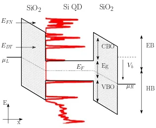
A special issue not always taken into account in the description of electronic transport is how the own potential of the nanostructure influences its elec-tronic states (was explained in Section 2.3). From a schematic point of view, electronic transport between one side and another side of the device takes place because there are occupied states with electrons on one side and avail-able states without carriers on the other side, the distribution of the electronic states being described by the density of states (DOS) of the material. In a general view, the potentialU shifts the DOS of the device while the electro-chemical potentialμ sets the energy where there are electrons. Thus,μ−U
gives an idea of which are the really filled states [15]. This mechanism is taken into account in the transport calculations of this PhD Thesis, and it is one of the main differences with respect to other previous transport studies of nanodevices.
The program used to compute the transport in this PhD Thesis, SIMQdot, was created by Sergio Illera and coded with MATLAB©. The basis of the code can be found in the following papers: basic transport mechanisms be-tween QDs in series or in parallel with constant transition rates and one level per QD [33], comparison of the methodology with NEGFF and exten-sion of the model to an array of multiple QDs [34], detailed explanation of the code with the capability of using WKB approximation to describe the tunnel transmission and of using more than one state per QD, in particular the solution of the Schr¨odinger equation for a particle inside a spherical well inside the effective mass approximation (EMA) [35], and, finally, how to cou-ple the electron transport with optical transitions due to incident light, like the situation in a solar cell device [36].
1.2
Brief overview of silicon quantum dots,
electronic transport and the present work
knowledge, the unique computations of transport in an extended array have been done by: (1) Carreras et al. [41], which use a semi-empirical tunneling current model, (2) Han et al. [42] and (3) Aeberhard et al. [43] employing one energy level per QD and NEGFF; and (4) Taranko et al. [44] using one energy level per QD and the equation of motion method.
On the other hand, one of the natural descriptions of a QD inside TH for-malism is as a particle inside a three dimensional square [45] or spherical [35] potential well. The main advantage of this description is that it allows de-scribing arbitrarily big QDs.
However, our porpoise in this PhD Thesis was to take also into account the influence of the surrounding dielectric matrix and impurity atoms on the transport properties, and this features are provided through fully ab initio
DOS. The earliest theoretical works of tunneling transport shown that one has to assume the density of states of the material as one of the main rele-vant factors in the calculation in order to correctly describe the experimental data [46]. Hence, we thought necessary,specially in the nanoscience field, to combine the performance of TH formalism with the accuracy of DFT for a deeper insight into the material properties. For example, DFT calculations shown that the relationship between energy gap and diameter in embedded Si QDs slightly differ from the predictions of the particle-in-a-box approxi-mation: DFT also shows modulations related to the oxidation state of the QD and the strain induced by the matrix [47].
Moreover, the proposed model can be efficiently coded in order to allow the computation of arbitrary large arrays of multiple QDs [35]. This can be simply done within the adopted formalism by taking into account the capac-itive coupling and the transmission coefficients between the QDs.
Doping Si QDs
Doping is essential in opto-electronic devices as a way to improve the mech-anisms to dissociate electron-hole pairs. P- and n- doped Si QDs in a SiO2
matrix have already been achieved showing electrically activated impurity atoms located in substitutional sites which enhance the conductivity with respect to undoped samples [3, 53–56]. Previous studies show that doping a nanostructure can be totally different than a bulk system [57–59], preventing the direct application of the wide knowledge of standard doped semiconduc-tors to nanostructures. Moreover, the promising new advances in experimen-tal techniques to dope Si QDs as small as 2 nm [60] in a controlled way open the possibility to start overlaping the theoretical and the experimental size regimes.
In particular, a nanoscale p-n junction formed by doped Si QDs embedded in a dielectric matrix has been proposed by several authors as the basis of a third generation of solar cells [61, 62]. However, further optimization is needed in order to improve the present solar cell characteristics, such as the open circuit voltage and the low current densities (tens of microamperes per square centimetre) [10].
However, to our knowledge, theoretical studies have only been done on free-standing Si QDs [57, 58, 63–68]. With this PhD Thesis, we want to start to complete the knowledge with doping Si QDs embedded in dielectric matrices.
About the applicability of DFT results
been identified as the most suitable for multiple-exciton-generation (MEG) processes, which is a highly desired condition in photovoltaic cells [72]. Re-garding the confinement energy, several experimental measurements of Si QDs embedded in SiO2 have shown that, even in the small QD limit, the gap never exceeds 2-3 eV [73].
1.3
Aim of this PhD Thesis
This Thesis initiated a collaboration between our group and the group of Prof. Ossicini of the University of Modena and Reggio Emilia, who has been modeling Si QDs for the last five years [47, 74–79]. In this context, we con-tributed with the capacity to study the transport properties of these models by taking advantage of mixing two different techniques, TH and DFT, which seems to open a really wide range of applications. In this PhD thesis we have only covered a single Si QD inside SiO2 matrix, but one could in principle
expand the procedure in order to explore the transport of an array of Si QDs, different dielectric matrices, include the interaction with light or with phonons, design transistors, memristors or thermoelectrics, etc. This PhD thesis provides the first steps of a procedure which seems to have no limits!
Thus, the aim of this work was to develop an approach to study transport in nanostructures by taking advantage of the atomistic information that ab initio methods can provide. After dealing with NEGFF, we finally decided to use TH technique for transport characteristics, much simpler than NEGFF but with similar results in the limit of weak coupling between the central active region and electrodes [34]. Thus, in this PhD Thesis we developed an approach that mixes DOS from a DFT calculation, allowing to use realis-tic states per QD, with TH formalism, trying to get the best characterisrealis-tics from each framework. In particular, the transport through a single Si QD embedded in a SiO2 dielectric matrix and the influence of the Si QD size, the
amorphization level, and the doping were studied.
1.4
Outline
This PhD Thesis is organized as follows:
explained.
In first place, concerning results, the DFT-NEGFF methodology was tested in Chapter 3. In this Chapter, a thermodynamic study of the stability of two polymorphs of Si depending on the size of Si nanowires was presented. Secondly, we studied the electronic transport proper-ties of these two polymorphs of bulk Si in the main crystallographic directions of growth of Si nanowires.
In second place, the study of electronic transport through a single Si QD embedded in a SiO2 matrix is presented in Chapter 4. Firstly, the
methodology DFT-TH proposed is widely studied, specially related to the parameters used in SIMQdot. Secondly, the influence on electronic transport of size and amorphization level of Si QD is showed.
In third place, in Chapter 5, the extrinsec properties of the systems pre-sented in the previous Chapter are studied. The p-doping (n-doping) was modelled by substituting a Si atom by a B (P) atom, in different possible impurity positions. The formation energy and structural and electronical properties are described in a first place, followed by the study of the electron current for n-doped systems and the hole current for the p-doped ones.
Finally, a Chapter 6 with the conclusions of this PhD Thesis and a special section with possible ideas to extend the here-present work are provided.
The research leading to this PhD Thesis has been published in the following papers:
A combination of the thermodynamical study of Si NWs stability (Sec-tion 3.2) and the electronic transport calcula(Sec-tion of bulk Si (Sec(Sec-tion 3.3) was published in Ref. [80]: “Stability Model of Silicon Nanowire Poly-morphs and First-Principle Conductivity of Bulk Silicon”.
The presentation of the methodology with the dependence of transport properties on the Si QD size and amorphization level was published in Ref. [81]: “Silicon quantum dots embedded in a SiO2 matrix: From
Theoretical framework
The aim of this chapter is to provide a brief description of the theories un-derlaying the codes used in the present work to investigate our systems of interest. Theab initio code SIESTA based in the Density Functional Theory (DFT) was used for the morphological and electrical properties, while, for the transport properties, two different approaches were used, Non-Equilibrium Green Functions Formalism (NEGFF) with ab initio code TranSIESTA and Transfer Hamiltonian (TH) formalism as implemented in SIMQdot code.
2.1
Density Functional Theory
The purpose of Condensed Matter Physics is to describe real materials through the motion and interactions of the atoms that compose them, i.e. by solving the Schr¨odinger equation of the system. Commonly, due to the huge number of interactions involved and the difficulty to solve the interaction between many-body objects, this would be a tough task to carry out. Several theories have been developed during the last decades in order to find a simplifica-tion of the descripsimplifica-tion of complex materials, being Hartree-Fock (HF) and Density Functional Theory (DFT) the most widely used. The latest one has been the commonly used for the description of semiconductor materials.
2.1.1
Some words about Hartree-Fock, correlation and
exchange
Hartree-Fock (HF) theory manages the incapacity to solve the exact interac-tion between the electrons of a many-body system by describing their energy as the sum of the direct and exchange terms of the electron-electron inter-action (Eq. 2.2). In this way, the self-exchange energy correctly cancels the self-Coulomb energy. It is a good method for systems where the high-density of the inner-shell electrons is important, like metals. However, the correlation energy is neglected in this theory and, although its contribution is small in the mentioned high density regime, HF is not suitable for systems where the low-density of valence electrons is significant, for which correlation may be as important as exchange [83]. In this context, DFT, which describes both exchange and correlation interaction, is more appropriate for semiconductor materials where the valence electrons are the protagonists. Moreover, it is also more desirable for large systems, where the combination of Slater deter-minants in HF would demand a huge computational effort.
The Hamiltonian for a many-body interacting system with Ne electrons in
coordinates {rrri} and Nn nuclei in coordinates {RRRI} with atomic numbers
{ZI} and mass {MI} is, in atomic units1:
ˆ
H =−1
2 Ne i ∇2 i − 1 2 Nn I 1
MI∇ 2 I − Ne i Nn I ZI
|rrri−RRRI|
+ 1 2 Ne i Ne
j=i
1
|rrri−rrrj|
+ 1 2 Nn I Nn
J=I
ZIZJ
|RRRI−RRRJ|
(2.1)
With the Bohn-Oppenhaimer approximation (explained in Section 2.1.3), the electronic part of the Hamiltonian used in the HF approximation is:
ˆ
He =−
1 2 Ne i ∇2
i +Vext+ Ne
i<j
1
|rrri−rrrj|
and the energy of an interacting homogeneous electron gas is: [84, 85]
1In atomic units, the numerical values of the following fundamental constants are all the unity: electron massme, elementary chargee, reduced Planck’s constant=2hπ, and
Coulomb’s constant 4π1
EHF = Ne
i=1
i|H0(i)|i+
1 2
Ne
i,j
⎡ ⎢ ⎢ ⎢ ⎣ij|
1
|rrri−rrrj|
|ij
direct term
− ij| 1
|rrri−rrrj|
|ji exchange term ⎤ ⎥ ⎥ ⎥
⎦, (2.2)
where the wave functions of the system |i are Slater determinants.
By using plane waves, one can see that the eigenvalues of this equation are plane waves with the free electron energy augmented by the exchange term
(kkk) = k
2
2 −
kF
π f(x)
where x=k/kF, the Fermi wave vector kF = (3π2n)1/3,n is the electron
den-sity, and f(x) = 1 +1−2xx2ln|1+1−xx|.
Exchange interaction arises from Pauli exclusion principle where electrons are antisymmetric and cannot have the same space position and spin value, so, electrons with parallel spins tend to go away one from each other, thus, reducing the Coulomb repulsion. Hence, the exchange term contributes to lower the system energy.
The total energy per electron in the HF approximation is calculated as the sum of single electron energies (kkk) corrected by half of the exchange term
x(kkk):
EHF/Ne =
2 Ne k k k
(kkk) + 1 2Ne
k k k
x(kkk) (2.3)
where the total energy exchange per electron, for each spin channel σ is:
σx = E
σ x
Nσ e
=− 3 4πk
σ
F =−
3 4 6 πn σ
1/3
(2.4)
errors leading to a successful description of systems (typically, DFT overes-timates exchange but underesoveres-timates correlation effects).
The correlation energy, thus, is defined as the difference between the total exact energy and the HF energy, i.e. kinetic energy and exchange energy. In a general view, Pauli exclusion principle also gives a correlation in electrons’ motion which is a result of the collective behavior of the electrons to screen and decrease the Coulomb interaction. Differently from the exchange term, the correlations are more important for electrons with opposite spins, be-cause they are more likely to occupy nearby positions.
Exchange and correlation describes the effect of electron-electron repulsion, i.e. the presence of an electron inrreduces the probability of finding another electron in r. As both the exchange and correlation terms tend to keep electrons apart, one can describe the exchange and correlation contributions in terms of a hole surrounding each electron and keeping the other electrons from approaching it. The so called exchange-correlation (XC) hole is related to DFT by an adiabatic connection set by Harris [86]. Moreover, the dif-ference description of electrons interaction by Hartree and XC contributions can also be interpreted as the separation between short-range and long-range Coulomb effects.
2.1.2
About Density Functional Theory
Hohenberg and Kohn [87] in their famous paper of 1964 together with the paper of Kohn and Sham one year later [88] set the basis of the density functional theory (DFT), that worth the Nobel Prize of Chemistry to W. Kohn in 19982. They extended the idea that Thomas [89] and Fermi [90]
already had in the decade of 1920: is there a way to condensate all the degrees of freedom information present in the wave function of an interacting many body system into only one parameter, the electronic density? Hohenberg and Kohn (H-K) derived the theory that we use nowadays [87]:
Given an interacting electron gas with an electronic density
n(rrr) in an external potential v(rrr), there exists a universal func-tional of the densityF[n], independent of v(rrr), with a minimum energy valueE ≡ v(rrr)n(rrr)drrr+F[n] equal to the correct ground-state (GS) energy associated to v(rrr).
The GS is found by the minimization of the energy functional with the constrain n(rrr)drrr=N, N being the number of elec-trons in the system.
Moreover, all the GS properties of a system can be completely de-scribed by its electron density, and the potentials can be written only as functionals of n(rrr).
Kohn and Sham [88] (K-S) provided the self-consistent scheme to convert the interacting many-body problem into a set of non-interacting single particle equations that are the ones implemented in the ab initio codes available at the moment.
From the H-K theorem it is formally possible to replace the many-electron problem by an exactly set of self-consistent one-electron equations by using an effective one-particle potential
vxc≡ δEδnxc(rrr[n)] in the equations and an universal functional3 G[n]≡
Ts[n] +Exc[n] in the energy variational principle. An explicit form of vxc can only be obtained if the exact functionalExc with
all many-body effects included is known. This effective potential will, then, reproduce the exact density of the system, and the total energy will be
E = N i=1 i− 1 2
n(rrr)n(rrr)
|rrr−rrr| drrrdr
rr+Exc[n]−
vxc(rrr)n(rrr)drrr,
(2.5) where i are the eigenvalues of the K-S equations (Eq. 2.6).
In other words, with H-K theorem and K-S equations, the interacting system is now a system of non-interacting electrons moving in the effective one-body potential vef f(rrr) = v(rrr) +u([n], rrr) +vxc([n], rrr), where u([n], rrr) =
drrr|rrrn−(rrrrrr)|
is the direct Coulomb potential and vxc([n], rrr) = δEδnxc(rrr[)n] is the
exchange-correlation potential. The equations to solve are, now ,the K-S equations, in atomic units:
3G[n] is related to the universal functional F[n] of the H-K theorem by substracting the classical Coulomb energy: F[n] = 12 n(|rrrrrr)−nrrr(rrr|)drrrdrrr+G[n]. Ts[n] is the kinetic energy
of a system of non-interacting electrons with density n(rrr), while Exc[n] is the exchange
−1
2∇
2+v
ef f(rrr)
ψi(rrr) = iψi(rrr). (2.6)
As we don’t know the exact form of the exchange-correlation functional, K-S provided two approximations to described it:
1. Local Effective Potential
If the density of the system is sufficiently slowly varying, the exchange and correlation term of the Eq. 2.5 can be substituted by the corre-sponding uniform electron gas term by
Exc[n] =
n(rrr)xc(n(rrr))drrr, (2.7)
where xc(n(rrr)) is the exchange and correlation energy per electron of
a uniform electron gas of densityn.
2. Nonlocal Effective Potential
To include exchange effects exactly, we can use
Exc[n] =Ex[n] +
n(rrr)c(n(rrr))drrr, (2.8)
where Ex[n] is the exchange energy of a HF system with density n
(Eq. 2.4) andc(n(rrr)) is the correlation energy per particle of a
homo-geneous electron gas.
The K-S paper set, then, a self-consistent procedure, called self-consistent field (SCF) method, to compute the density matrix (see Fig. 2.1 for a schema):
1. Assumption for n(rrr)
2. Construction of ϕ(rrr) from Eq. 2.10 and of μfrom Eq. 2.11 or Eq. 2.14
and the total energy of the system by leaving all the many-body effects in the functional Exc[n]
E =
v(rrr)n(rrr)drrr+ 1 2
n(rrr)n(rrr)
|rrr−rrr| drrrdr
rr+Ts[n] +Exc[n]. (2.9)
For the Local Effective Potential approximation,
ϕ(rrr) =v(rrr) +
n(rrr)
|rrr−rrr|drrr
(2.10)
and the exchange and correlation contribution to the chemical potential of a uniform gas of density n is
μxc(n) = d(nxc(n))
dn (2.11)
In this context, the densitynis obtained by solving the one-particle Schr¨odinger equation
−1
2∇
2+ϕ(rrr) +μ
xc(n(rrr))
ψi(rrr) = i(rrr)ψi(rrr) (2.12)
and setting
n(rrr) =
N
i=1
|ψ(rrr)|2. (2.13)
However, for the Nonlocal Effective Potential approximation,
μc(n) =
d(n c(n))
dn (2.14)
and the equation to solve is now
−1
2∇
2+ϕ(rrr) +μ
c(n(rrr))
ψi(rrr)−
n1(rrr, rrr)
|rrr−rrr|ψi(rrr
)drrr =
i(rrr)ψi(rrr) (2.15)
where n1(rrr, rrr) =
N
j=1
ψj(rrr)ψj∗(rrr) is the one-particle density matrix as defined
n(rrr) =
occ|
φi(rrr)|2 →nμν =
occ
cμiciν
Compute electron density
?
−1 2∇
2+v
ef f(rrr)
ψi(rrr) =iψi(rrr)→( ˆH)(C) = E( ˆS)(C)
Solve the KS equations
?
vef f(rrr) = v(rrr) +u([n], rrr) +vxc([n], rrr)
Calculate the effective potential
? n(rrr) Initial guess
6
Convergence of n(rrr)?
a a a a a
!!!!!aaaaa!
! ! ! !
No
Figure 2.1: Schema of the self-consistent field cycle (SCF) in DFT calculations.
Exchange-Correlation Functional approximation: LDA and GGA
The exchange-correlation functional is only known for the free electron gas case [87]. For the other systems, two main approximation are used [91]: the Local Density Approximation (LDA) and the Generalized Gradient Approx-imation (GGA).
LDA (Eq. 2.7) approximates the exact exchange-correlation potential by its solely linear dependence on the electron density. It was presented by Ceper-ley and Alder [92] and it is normally used under the parametrization done by Perdew and Zunger (PZ) [83] or Perdew and Wang (PW92) [93].
In this way, the results of many-body calculations for the homogeneous sys-tem [92, 94] can be used into calculations for inhomogeneous syssys-tems. By construction, LDA becomes exact when the densities vary slowly enough on the scale of the local Fermi wave length λF = 2π/kF and the screening
Moreover, the parametrization of Perdew and Zunger [83] introduced a method for considerably improving the LDA results by subtracting the self-interaction energy, which emerges because there is not an exact cancellation between the direct and the exchange term in DFT.
Hence, Ceperley [94] established the parametrization for any density as, be-ingrsthe Wigner-sphere radius in units of Bohr radii related to the electronic
density by n−1 = 4 3πr
3
s:
1. Exchange energy
Ex =−
3 4
3
π
1/3
n(rrr)4/3drrr (2.16)
2. Correlation energy at low density regime,rs ≥1
c =γ/(1 +β1
√
rs+β2rs) (2.17)
3. Correlation energy at high density regime, rs <1
c =Alnrs+B+Crslnrs+Drs (2.18)
where the values for the different constants can be found in Ref. [83, 93, 95].
The local spin-density approximation (LSDA)
ExcLSDA[nup, ndown] =
xc(nup, ndown)n(rrr)drrr (2.19)
is used to explicitly take into account both spins in the calculation. An ac-curate description forxc(nup, ndown) has been constructed from Monte Carlo
simulations of jellium by Perdew et al. [83, 93].
of the density into the exchange-correlation functional, as it is done in the Generalized Gradient Approximation (GGA):
ExcGGA =
drrrf(n(rrr,∇∇∇n(rrr)) (2.20)
where the choice of the functionf yields to the different GGA flavors. One of the most used is the parametrization done by Perdew, Burke and Ernzerhof (PBE) [97], where all parameters are fundamental constants, trying to sim-plify previous GGA parameterizations and, moreover, looking for retaining the correct features of LSDA combining them with the most energetically important features of gradient-corrected nonlocality.
A particular parametrization used in Section 3 is PBEsol [98] that was specif-ically constructed to improve the lattice parameter of solids, and therefore other equilibrium properties related to it such as bulk moduli, phonon fre-quency or ferroelectricity, and jellium surface exchange energy of solids and surfaces.
Potentially more accurate exchange-correlation functionals are
1. The meta-GGA that also includes the second derivative of the electron density [99].
2. The hybrid-functionals, where the exchange part of the energy func-tional is a mixture of the exact exchange energy calculated from HF theory and a DFT exchange functional [100] leading to Nonlocal Effec-tive Potentials (Eq. 2.8) in the case of using onlyEX from HF.
2.1.3
Approximations in present DFT computations
and notes about the code
all electron calculations normally local orbitals are used, whereas pseudo po-tential methods normally use PW. However, SIESTA [101, 102] is faster than other DFT codes because mixes both, local orbitals (basis set is numerical pseudo atomic orbitals of finite range) and pseudo potential approximation.
1. Bohn-Oppenhaimer approximation: decoupled movement of electrons and nuclei due to the difference in mass between them. We can consider that the kinetic energy for nuclei is much lower than the electrons kinetic energy, so nucleus are considered frozen, only the kinetic energy of electrons is taken, and the Coulomb interaction between nuclei is then fixed as an external potential.
2. Description of the exchange-correlation term of the K-S equations: as has been explained in the previous section, an approximation to the exchange-correlation potential is needed. In this PhD dissertation we used LDA and GGA, depending on the size of the systems studied.
3. Pseudo potential: Herring [103] noticed that, usually, it is not neces-sary to include core electrons in calculations (the core states of a solid are quite similar to those in the free atom and slightly change under electrical perturbations), so we use the so-called pseudo potential ap-proximation, where only the valence electrons are explicititly used in the computation. To achieve the separation between core and valence electrons, one replaces the true all electon potential VAE by a pseudo
potential VP S, that, applied to the pseudo wave functions, gives the
same eigenvalues than the original atomic potential. After computing the all electron wave functions for the valence electrons of the specie under study, one creates a pseudo wave function, where the strong os-cillations due to the core states are smoothed out before a certain core radiusrc (see Fig. 2.2) but it matches the all electron wave function
af-ter it. The corresponding pseudo potential matches the true potential outside the core radius.
Differently from true wave functions, where the eigenfunctions of the valence electrons |ψ are orthogonal to the core states |cproduced by the same potential VAE, because of pseudo wave functions |φ do not
Figure 2.2: Wave function for an all electron calculation (black dot line), pseudo wave function which does not have the orthogonal part of the core electrons beforerc (black solid line), Coulomb potential
(red dot line), and the generated pseudo potential (red solid line).
in terms of smoothly functions, the idea is to create a new pseudo wave function with the same eigenvalue of the valence state but without the restriction of orthogonality with the core states and that is equal to the original wave function after a certain cutoff radius.
(T +VAE)|ψ=|ψ
(T +VAE)|c=c|ψ
⇒ ψ|c= 0
|ψ=
I−
c
|cc|
|φ (2.21)
(T +VAE)
I−
c
|cc|
|φ=
I−
c
|cc|
|φ
T +VAE+
c
(−c)|cc|
|φ=|φ
(T +VP S)|φ=|φ
4. Basis sets: The wave functions of a system are normally expanded in a basis set in order to save computational time because computing coefficients is a much easier task than finding the wave functions value over all range of coordinates.
φi(rrr) =
α
ciαfα(rrr) (2.22)
Two kinds of basis sets can be found in ab initio codes: not localized (PW) or localized (atomic orbitals, being gaussian or numerical). The first one is considered most accurate and it has the advantage of us-ing only one parameter for its description: the cutoff energy or the maximum kinetic energy that the PW can have. Also, PWs have the same accuracy in all the space. However, hundreds of PW are com-monly needed per each atom in order to have a proper description of a system. For the last reason, localized basis set are commonly used due to the low number of basis functions needed to have similarly preci-sion. In particular, SIESTA uses a lineal combination of atomic orbitals (LCAO) as a basis set:
φIlmn(rrr) =RIln(|rrrI|)Ylm(ˆrrrI), (2.23)
where RIln is the radial part expressed in terms of numerical pseudo
atomic orbitals with finite range, defined by their size (number of or-bitals for a given l m n), range (spatial extension of the oror-bitals), and shape of the radial part. Ylm is the angular part in terms of spherical
harmonics.
atomic orbitals (NAO) to describe wave functions, i.e. it solves numer-ically the radial part of the Schr¨odinger equation of the atom.
The size of the basis set is the number of radial functions per atom used and it could be single-ζ, i.e. one radial function per atom, or multiple-ζ, which lets the possibility to be flexible in the radial part. Finally, in order to allow a proper description of effects perturbing the symmetry of the electron density, an angular flexibility can be added to the basis set with a polarization orbital, i.e. to let the atom to have more angular momentum.
Higher size of basis set goes to the PW value of energy inside the approximation of the pseudo potential and functional of your calcula-tion [101]. For the atoms used in this PhD dissertacalcula-tion, the DZP is commonly used in all the studies found in literature.
In spite of their improvement of computational time, some issues con-cerning the use of atomic orbitals can arise, but they can be solved using enough accuracy, i.e. by increasing the basis set size of the sys-tem under study. As an example, one of the known problems intrisic to local basis set is the basis set superposition error (BSSE), proce-dent from the fact that LCAO are centered on the atom instead of being homogeneus like PW. The quality of the basis is, then, geome-try dependent and may lead to overstimation of the interaction energy between different species of the system.
Among the physical properties that DFT codes provide, in this PhD Thesis we were interested in:
Total K-S energiesEKS
Eigenvalues of the K-S equationsi and wave functionsφi(rrr) Density of states (DOS):g() =
i
μ
ν
cμiciνSμνδ(−i)
Projected density of states (PDOS), which corresponds to the DOS projected in the orbital μ:
i
ν
cμiciνSμνδ(−i), being the overlap
matrix S=φν|φμ because of the use of nonorthogonal basis set.
Mulliken population, which is an estimation for the partial atomic charge: Pμν =DμνSμν, in terms of the density matrixDμν = 2
where the sum has been done over the molecular orbitals of each basis function.
2.2
Non-Equilibrium Green Functions
Formal-ism
When one poses the study of transport at the nanoscale some challenges emerge, such as how to deal with open systems, i.e. infinite systems but with non-periodic boundary conditions, how to describe non-equilibrium condi-tions, like a system with two different electrochemical potentials, or how to describe the interface between the contact and the device region. All this issues can be treated with NEGFF, and its implementation in codes such as TranSIESTA allows also to use the ab initio description of DFT to study nonperiodic systems, such as an atomic or molecular-scale system (the con-tact or central C scattering region) connected to two semi-infinite left (L) and right (R) electrode regions at different electrochemical potential. Thus, TranSIESTA code [26] uses the Keldysh formalism [106] to compute the elec-tronic transport properties only in a finite region (L+C+R) of the infinite system.
2.2.1
Description of nanodevices inside NEGFF
NEGFF is based in the retarded GF GR and the lesser GF G< of a system, also known as particle propagator, which describes the density of available states and how electrons occupy those states, respectively [17]. In a DFT-NEGFF framework, the retarded GF of a system is obtained by inverting the DFT Hamiltonian H and using the overlap matrices S from a given electron density, GR(E) = (E·S−H)−1.
Self-energies or how to solve the coupling with electrodes
Hence, the retarded device GF GR
D is written in terms of the retarded GF
of the isolated electrodegR (see Eq. 2.27) and the problem of describing the
coupling of the device to the reservoirs is reduced to the calculation of the contact GF, which is only needed to be known in the vicinity of the device, simplifying the computation with surface GF methods [22].
How to deal with open boundary systems: device and electrode Hamiltonian
GFs can describe non-periodic systems if we are able to separate the system Hamiltonian into two subsystems and write it as an unperturbed partH0and
the interaction between the two subsystemsV,H =H0+V. The expressions
of the unperturbed Hamiltonian and the interaction are:
H0 =
HD 0
0 HE
;V =
0 V
V+ 0
(2.24)
HE being the Hamiltonian of the electrode andHD of the device subsystems.
The corresponding unperturbed GF is known:
G0 = (EI−H0)−1 =
⎛
⎝(EI−HD)
−1 0
0 (EI−HE)−1 gR
⎞
⎠. (2.25)
From the Dyson equation,
GR(E) =
GRD GRDE GR
ED GRE
=G0(E) +G0(E)V GR(E), (2.26)
we can write the retarded GF of the deviceGR
D only in terms of the retarded
GF of the isolated reservoir gR, by using the expression GR
ED =gRV+GRD:
GRD = [EI−HD−V gRV+]−1 = [EI−HD −ΣR]−1 (2.27)
which defines the retarded boundary self-energy,
ΣR=V gRV+, (2.28)
In conclusion, the non-hermitian matrices ΣL,R(E) represent the retarded self-energies for the left (L) and right (R) electrode, and can be seen as the escape rates of electrons from the active region into the semi-infinite ideal electrodes, so that an open quantum system can be described by the non-hermitian Hamiltonian Hopen = H0 + ΣL(E) + ΣR(E). The matrices
ΓL,R(E) = i[ΣL,R(E) −Σ+L,R(E)] describe the level broadening due to the
coupling to the electrodes.
2.2.2
Expressions used in TranSIESTA code
Due to the finite basis set used in TranSIESTA, the system Hamiltonian (Eq. 2.29) can be separated into three independent parts: the contact region (C), and the left (L) and right (R) electrodes.
HT ranSIEST A=
⎛
⎝HLV+ ΣCL L VHLCC VCR0
0 VRC HR+ ΣR
⎞
⎠ (2.29)
Specially important is the use of bulk electrode values in the L,R parts (Hamiltonian matrices HL,R and self energies ΣL,R) of the system
hamil-tonian from a separately previous bulk calculation of the electrodes with periodic boundary conditions, as will be explained below.
The one corresponding to the interaction between electrode-contact region
VLC,RC and the Hamiltonian of the contact region HC are both computed
explicitly with TranSIESTA GFs in an open boundary system.
Calculation of the density matrix
The computation of the density matrix is different depending on whether it is an equilibrium situation, i.e. at zero bias voltage, or a non-equilibrium one, i.e. at finite bias.
1. At equilibrium
The integration of the lesser GF over energies determines the density matrix by,
Dμν =
1 2πi
dEG<μν(E) = ∞
−∞
wheref(E) is the distribution function of the system, μF the chemical potential, and the spectral density matrix can be written as
ˆ
ρ(E) =−1
πIm[G
R(E+ iδ)]. (2.31)
In the coherent transport regime, i.e. when electron-phonon or phonon-phonon interaction are not taken into account,G<(E) can be expressed only in terms ofGR(E) = [E·S−H−Σ
L(E)−ΣR(E)]−1.
For a given finite base set φ(rrr), the density matrix in the real space is
ρ(rrr) =
μν
Dμνφμ(rrr)φν(rrr). (2.32)
2. At non-equilibrium
When a finite bias voltage is applied, a difference between the left (μL)
and right (μR) electrochemical potential appears and a current flows
leading to a non-equilibrium situation. A description of the electro-static potential is, then, needed.
In TranSIESTA code it is written as:
VH(rrr) = ϕ(rrr) +aaa·rrr+b (2.33)
where ϕ(rrr) is a solution of the Poisson’s equation for a given electron density.
The linear term is determined by imposing boundary conditions: the left electrode is at a voltage +Vb/2 and the right electrode at −Vb/2,
the bias voltage applied beingeVb =μL−μR. Thus, the linear term is
−Vb
L
z− L2,L being the distance between electrodes.
The scattering states from the left electrode, similar for the right elec-trode, can be written in basis of the equilibrium wave function ψ0
L(xxx)
by
ψL(xxx) = ψL0(xxx) +
dyyyGR(xxx, yyy)VLψL0(yyy). (2.34)
Dμν =
∞
−∞
dEρLμν(E)f(E−μL) +ρRμν(E)f(E−μR) (2.35)
where the spectral density matrix is defined by
ρLμν(E) = ⎡ ⎣GR1
πIm [ΣL]
ΓL
(GR)+ ⎤ ⎦
μν
. (2.36)
For an extended derivation of the equations see the Appendix A.
Calculation of the current in a nanodevice
TranSIESTA computes the elastic scattering by the potential of the device region. It does not treat the inelastic scattering due to electron-electron interaction, i.e. Coulomb blockade, phonons impurities, or other inelastic scattering centers.
The Landauer formalism sees the conductance of a quantum device as the transmission probability to go through this region [15, 107]. Moreover, it assumes that electrons are non-interacting particles, that the electrodes are perfect crystalline, i.e. there is no scattering inside the leads, that the elec-trons incident from the left (right) electrode are in thermal equilibrium with the left (right) reservoir of electrons, and that there is no back-scattering at leads interface.
Thus, under Landauer-Buttiker formalism, the transmission spectra is:
T(E) = Tr[t+t], (2.37)
t being the transmission matrix, i.e.ψout=t ψin.
The current flowing from the left to the right electrode due to a bias voltage applied Vb, is related to the probability to have transmission in this bias
window μL−μR:
I(Vb) =
2e h dE −∂f ∂E
T(E, Vb) (μL−μR)
= 2e
h
where the derivative of the equilibrium Fermi distribution f(E−EF) is ap-proximated by ∂E∂f ∼ −f(E−μL)−f(E−μR)
μL−μR and fL,R(E) = f(E −μL,R) are the
Fermi-Dirac distribution functions of the left and right lead, respectively.
In NEGFF the transmission coefficient is computed from the self-energy and the GF of the finite system by
t(E) = (Im[ΣR(E)])1/2GR(E) (Im[ΣL(E)])1/2
= (ΓR(E))
1/2
GR(E) (ΓL(E))
1/2
. (2.39)
Procedure for computation
First of all, a finite region is needed to be described in order to perform the computation. From the GF of the infinite system
G(E) = ⎛ ⎜ ⎜ ⎜ ⎜ ⎝
... −VL+
−VL− E·S−HL −VLC
−VCL E·S−HC −VCR
−VRC E·S−HR −VR+
−VR− ...
⎞ ⎟ ⎟ ⎟ ⎟ ⎠ −1
by defining a finite region with part of the left and right electrodes and the contact region, the GF of the finite system can be written as
G(E) = ⎛
⎝E·S−−HVCLL−ΣL E·−SV−LCHC −V0CR
0 −VRC E·S−HR−ΣR
⎞ ⎠ −1 , where #
ΣL=VLgRLV
+
L
ΣR=VRgRRV
+
R
(2.40)
are the self-energies of the leads which describe the coupling of the explicit atoms used in the calculation of the finite system to the remaining part of the semi-infinite electrode through the unperturbed surface electrode GF gR
L,R.
and VR used to construct the self-energies ΣL,R are only related to the inter-action between the bulk electrode and the electrode atoms that are explicitly in the finite region, not with atoms of the contact region. Thus, only elec-trode atoms are involved, and this quantities can be calculated from a bulk electrode calculation, a much more easy task.
The other term needed to compute ΣL,R, the unperturbed surface electrode
GF gR
L,R, is also taken in the first step of the TranSIESTA procedure, a bulk
calculation of the electrodes. The self-energies are computed from the initial bulk electrode calculation by cutting the bulk infinite electrodes into two semi-infinite systems and using either ideal construction [108] or efficient re-cursion method [109] to calculate the interactions.
Then, in a second step, a SCF cycle of the finite region is computed, and the Hamiltonian of the finite region (Eq. 2.29) is obtained from the GF rather than a normal diagonalization. With the GF, the density matrix is obtained from Eq. 2.30 and Eq. 2.35, which begins the SCF cycle again.
Finally, the transmission function is obtained with a post-processed tool, TBTrans [26], which uses the self-energies of the electrodes and the GF of the whole system (Eq. 2.39).
Figure 2.3: (top) From the infinite system (blue atoms in electrode goes to infinite) the finite region is the following: the selected atoms from the left L and right R electrode (red), and the central region C (yellow). (bottom) This finite region is a supercell with periodic boundary conditions in the TranSIESTA calculation.
As a conclusion, the main steps for a transport calculation inside TranSI-ESTA code are:
1. Definition of the system: electrodes + contact region (Fig. 2.3).
2. Periodic boundary calculation of bulk electrodes (left and right): HL,R,
ΣL,R and overlap matrices SL,R are computed from the K-S equation
at equilibrium. Hamiltonian and density matrix (DM) values for the electrodes in the finite system are fixed to these bulk values (c0
3. Open boundary calculation of the finite system L-C-R: HC, VLC and
VCRare computed in a supercell approach (See Fig. 2.3). Non-equilibrium
density matrix Dμν is computed from the non-equilibrium coefficients
clμ=
ν
(GV)μνc0 lν.
A SCF cycle starts:
(a) reads the electrode data
(b) builds H from the density matrix using K-S equations
(c) solves the open problem using GFs formalism,
G(E) = [EI−Htransiesta]−1
(d) builds new density matrix,
Dμν =
l
clμc∗lνnF(L−μL) +
r
crμc∗rνnF(R−μR)
(e) SCF cycle repeats steps (b) to (d) until convergence.
4. Transport calculation, post-processing tool TBTrans: computation of the electron current I at the bias voltage Vb using the Eq. 2.38 and
Eq. 2.39.
Considerations in the description of the system
Some considerations in the description of the system are needed in order to accomplish the approximations took in the computation.
1. The width of the bulk electrode cell has to be large enough in order to not have interaction between second neighbor cells
2. Central region C large enough in order to don’t have interaction be-tween left and right electrodes.
3. L and R leads large enough in order to don’t have interaction between C and the bulk region of the electrodes.
2.2.3
Exemple of the use of NEGFF in a transport
calculation
the retarded self energy ΣR can be seen as an energy broadening of the levels
inside the contact region, due to the contact region-lead coupling V. Being ΓL (ΓR) this broadening due to left (right) contact, the self-energy is written
as
ΣR=−iΓ 2;
being Γ = ΓL+ ΓR. In the special case of only one quantum dot, all the
matrices are scalar terms and, thus,
HC =1 ; ΣR =−
i
2(ΓL+ ΓR). The Green Function of the system is easily written as
GR= [E −HC −ΣR]−1 =
1
E−1+ iΓ2
Finally, the transmission coefficient is,
T(E) =T r[ΓLGRΓR(GR)+] =
ΓLΓR
(E−1)2+ Γ
2
4
We can see how the transmission coefficient of one QD has a lorentzian shape peaked at the energy level and with a line width equal to Γ, the QD-lead coupling strength.
The case of two QDs in series with energy levels 1 and 2 and a coupling
between themt12will have only the interaction between the first QD and the
left lead ΓL1 and between the second QD and the right lead Γ2R.
The broadening and corresponding retarded self-energy will be written as
Γ =
ΓL1 0
0 Γ2R
; ΣR =−i 2
ΓL1 0
0 Γ2R
The expression for the retarded Green Function is, then,
GR(E) =
E−1+2iΓL1 −t12
−t12 E−2+ 2iΓ2R
−1
2.3
Transfer Hamiltonian formalism
The code used for transport calculations through a silicon quantum dot is based on the Transfer Hamiltonian approach for the expression of the cur-rent, and on the WKB approximation for the expressions of the transmission coefficients.
2.3.1
Transfer Hamiltonian formalism:
transport in
quantum devices
Payne developed in his paper [20] the method to describe resonant tunnel-ing current by calculattunnel-ing the occupancy of the resonant level through an extension of TH previously adopted by Bardeen [46]. The TH technique is used to study the electronic tunneling transport through a barrier, based in the division of the tunnel junction into subsystems, each one consisting of a single electrode connected to a semi-infinite potential barrier (Fig. 2.4). In this sense, the attraction of the technique is its simplicity and that the description of transport is given in terms of the properties of only the uncou-pled subsystems with the electronic states of the electrodes as a perturbation into the device, with
⎧ ⎨ ⎩
H1ψ1 =1ψ1
H2ψ2 =2ψ2
HRψR=RψR
.
-
-ψin ψout
R 6
V(x)
= + +
H1 H2 HR
b a
Figure 2.4:Schema of the barrier in TH formalism and how it is divided into two subsystems containing each electrode and a semi infinite barrier.
The transition rate between initial states on one side of the barrier and final states on the other side is calculated from the Fermi Golden rule, and the matrix element for the transition is [20]
M1→2 =
2
2m
S
![Figure 1.1: (top) Reprinted with permission from [8]. Copyright 1992, AIP Publishing LLC.: Relationbetween free-standing Si QD diameter and band gap](https://thumb-us.123doks.com/thumbv2/123dok_es/5225873.95228/15.612.146.519.142.594/figure-reprinted-permission-copyright-publishing-relationbetween-standing-diameter.webp)