1
Electromagnetic enhancement effect on the atomically
abrupt heterojunction of Si/InAs heterostructured nanowires
J. L. Pura, 1* A. J. Magdaleno,1 D. Muñoz-Segovia,1 M. Glaser,2 A. Lugstein,2 J. Jiménez 1
1. GdS Optronlab, Dpt. Física de la Materia Condensada, ed. LUCIA Universidad de
Valladolid, Paseo de Belén 19, 47011 Valladolid, Spain
2. Institute for Solid State Electronics, Vienna University of Technology, Floragasse 7, 1040
Vienna, Austria
* Email: [email protected]
Abstract
Semiconductor nanowires (NWs) present a great number of unique optical properties
associated with their reduced dimension and internal structure. NWs are suitable for the
fabrication of defect free Si/III-V heterostructures, allowing the combination of the properties
of both Si and III-V compounds. We present here a study of the electromagnetic (EM)
resonances on the atomically abrupt heterojunction of Si/InAs axially heterostructured NWs.
We studied the electromagnetic response of Si/InAs heterojunctions sensed by means of
Micro-Raman spectroscopy. These measurements reveal a high enhancement of the Si
Raman signal when the incident laser beam is focused right on the Si/InAs interface. The
experimental Raman observations are compared to finite element methods (FEM)
simulations for the interaction of the focused laser beam with the heterostructured NW. The
simulations explain why the enhancement is detected on the Si signal when illuminating the
HJ and also provide a physical framework to understand the interaction between the incident
2
EM field and the heterostructured NW. The understanding of this process opens the
possibility of controlling the light absorption/scattering on semiconductor NWs with the use
of heterostructures, while taking advantage of the properties of both Si and III-V
semiconductors. This is important for current NW based photonic nanodevices, such as light
sensors, but also for the design of new optoelectronic devices based on NWs.
3
Introduction
Semiconductor nanowires (NWs) exhibit unique physical properties as a consequence of
their reduced dimension, the diameter. Besides, the presence of heterojunctions (HJ) is
necessary for building up electronic and optoelectronic nanodevices.1–4 Among all the
possible heterostructured NWs, those based on Si are especially interesting because of its
useful properties for solar applications, versatility and the possibility of their integration with
the already existing Complementary Metal Oxide Semiconductor (CMOS) technology.
According to this, a great variety of Si NW based devices has been produced, e.g. Si NW
near-infrared photodetectors5 or double-gated Si NW FET sensors.6 On the other hand, III-V
semiconductors present higher values of the carrier mobility and improved optical properties
with respect to their group IV counterparts, thus making up for Si drawbacks. The integration
of Si/III-V heterostructures in a single NW would allow combining the advantages of both
Si and III-V semiconductors with the unique optical properties of semiconductor NWs.7–10
III-V semiconductor NWs are being extensively investigated for its possible applications on
nanowire solar cells,11 and light sources, including lasers.12–14 There are excellent studies of
InP NWs, based on their optical properties and resonances,15 and its high efficiency as solar
cells.16 Also, as an example of Si/III-V integration, InAs NWs deposited on a Si substrate
were used in photovoltaics and photodetectors.17
In previous works, we reported the enhancement of the Raman signal at the heterojunction
of axially heterostructured Si/SiGe nanowires.18 We demonstrated that the enhancement
effect appears as a result of the interaction between the incident electromagnetic (EM) field
and the dielectric discontinuity at the heterojunction.19,20 According to this, the EM
4
work we will study the electromagnetic behaviour of heterostructured Si/InAs NWs using
micro-Raman spectroscopy as a probe of the EM field inside the NW. A theoretical
framework of the problem is established by solving the Maxwell equations of the light/ NW
system by Finite Element Methods (FEM). Finally, the results of the simulations are
contrasted with the micro-Raman experiments.
Experimental and Samples
The Si/InAs heterostructured NWs were fabricated with an ion implantation and flash
annealing procedure, similar to the one presented in reference 4. The 〈111〉 oriented Si NWs
were epitaxially grown on Si (111) substrates by applying the gold-catalyzed
vapour-liquid-solid (VLS) method. After removal of gold by wet chemical etching, approx. 20 nm SiO2
was deposited on the NWs by plasma enhanced chemical vapour deposition, acting as a
protecting layer for the following steps. In order to achieve homogeneous implantation
profiles along the NWs, samples were placed on a 45° tilted and continuously rotating stage
during ion implantation. In and As ions were implanted alternatingly with an energy of 120
keV and 90 keV, respectively. The recrystallization along with the phase separation and
formation of Si/InAs heterostructures within the NW core was finally achieved by applying
5
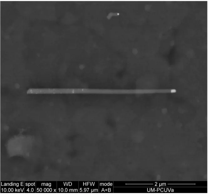
Figure 1. Backscattering SEM image of a typical Si/InAs heterostructured NW. The InAs
segment can be detected on the right side as a brighter region on the NW.
The NW morphology and structure were studied in a high-resolution Field Emission
Scanning Electron Microscope (FESEM). Heterostructured NWs appear as straight cylinders
with slight tapering. The InAs segment is shorter than the Si segment, namely 200 – 500 nm
vs 3 – 4 μm. Energy-Dispersive X-ray Spectroscopy (EDS) was used to determine the NW
6
while the darker contrast segment consists of Si, as expected from the different atomic
number (see Fig.1).
Figure 2. Typical Raman spectrum of a Si/InAs NW when the HJ region is illuminated. It
shows the principal Raman bands of both NW segments, Si and InAs.
Raman spectra profiles along the axes of several Si/InAs NWs were obtained in order to
study the effect of the heterojunction on the Raman signal. The Raman spectra were recorded
along the NW axis in steps of 200 nm. The details about the experimental method followed
for the characterization of the heterostructured NWs can be found elsewhere.18,19 The typical
Raman spectrum of these NWs when the HJ is being excited by the laser beam will contain
the Raman bands of both crystalline Si and InAs, Figure 2. When each individual segment of
7
NW segment consists of the degenerated LO and TO modes located at 520.6 cm-1, labelled
Si (LO,TO), and the much less intense second order transverse acoustic mode around 300
cm-1, labelled Si (2TA). For the InAs segment, we can observe the LO and TO modes at
217.3 cm-1 and 238.6 cm-1, respectively.21
Results
We acquired the Raman profiles along the axis of several Si/InAs NWs. Then, the intensities
of the different Raman bands were extracted from each spectrum. This allows visualizing the
dependence of the Raman signals as a function of the laser beam position along the NW. Two
examples of the Raman intensity profiles are shown in Figure 3, corresponding to two
different Si/InAs heterostructured NWs.
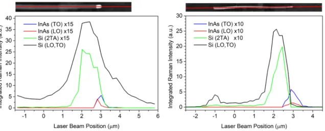
Figure 3. Raman intensity profiles of two different Si/InAs heterostructured NWs. The upper
backscattering SEM images show the profile path followed during measurements. A strong
enhancement of the Si signal arising from the Si region adjacent to the HJ can be seen.
Both profiles show that the Raman intensities arising from the Si segment are enhanced when
8
times, respectively. This enhancement factor is calculated as the ratio between the maximum
signal recorded next to the HJ, with respect to the Si signal recorded on the homogeneous Si
segment of the NW. This proves that the enhancement effect is also present in Si/InAs
heterostructured NWs, in spite of some differences with respect to the same effect observed
in Si/SiGe NWs previously studied.11,12 In the case of SiGe/Si heterostructured NWs, Si and
Ge are both non-polar semiconductors and the SiGe alloy is stable for any Si/Ge ratio. The
full miscibility of Ge and Si, and its high solubility in the catalyst metal, are responsible for
the graded HJs extending several tens of nanometres depending on the NW diameter.22 The
SiGe/Si heterojunction is not abrupt, but a continuous transition between the compositions
of the NW segments constitutes the heterojunction. Therefore, one can associate a certain
volume of material to the HJ region itself, which is chemically recognizable, and the Raman
signal arising from this volume forming the HJ permitted to study the true local field
enhancement (intensity per unit scattering volume). This situation does not apply to the
Si/InAs NWs, because the immiscibility between polar InAs and non-polar Si makes the
Si/InAs heterojunction atomically abrupt.23 For this reason, one cannot extract a spectrally
differentiated signal arising from the HJ itself; however, the EM enhancement effect is
clearly observed around the HJ in the profiles of Figure 3. The Raman intensity of Si is
strongly enhanced in the region of the Si NW segment adjacent to the heterojunction. The
true EM enhancement per unit scattering volume is difficult to estimate, because of the
limited spatial resolution of the micro-Raman probe. However, the increase of the Raman
intensity around the HJ can be unambiguously appreciated in Figure 3.
The experimental results have been contrasted with the EM field calculated by Finite Element
9
system, the FEM calculation provides us with the distribution of the electric field intensity,
|E|2, inside the NW. A more detailed explanation of the developed FEM model can be found
in previous papers.18,19 There are two main differences in Si/InAs heterostructured NWs with
respect to Si/SiGe heterostructured NWs. First, as we mentioned, the axial heterojunctions
for both types of NWs are different, graded for SiGe/Si and abrupt for InAs/Si. Second, InAs
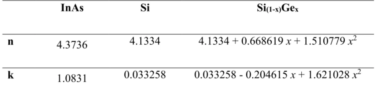
presents much higher dielectric losses (imaginary part of the refractive index, k) than Si or
the SiGe alloy for light in the visible range, Table 1. The values of the optical constants of
InAs can be found in Ref. 24.
Table 1. Real (n) and imaginary (k) parts of the complex refractive indexes of the different
materials used in the FEM calculations for 532 nm radiation
The main results of the simulations are summarized in Figure 4. The solution of the Maxwell
equations provides the distribution of the EM field inside the NW. Figure 4a shows the
volume distribution of the relative EM field intensity on the NW and its environment when
the laser beam is focused on the HJ. The relative EM field is defined as the value of the EM
field divided by the incident field, |E|2/|Einc| 2. Figure 4b shows the distribution of the same
magnitude along the NW axis. We can see that the effect of the higher dielectric losses on
the InAs side consists of a marked reduction of the EM field intensity with respect to the Si
side next to the HJ. It explains the low InAs Raman signal detected on the experimental
InAs Si Si(1-x)Gex
n 4.3736 4.1334 4.1334 + 0.668619 x + 1.510779 x2
10
measurements, even next to the heterojunction. On the other hand, we can see the
enhancement and localization of the incident field on the Si side. The EM field is enhanced
by more than 3 times in a small region of about 300 nm, close to the heterojunction. One can
establish here an estimation for the dimension of the NW region where the EM enhancement
takes place, therefore one can estimate the Raman intensity per unit volume to bring up the
true EM enhancement at the HJ. Figure 4c presents the theoretical Raman intensity, which
should be proportional to the excitation field intensity i.e. |E|2. This value is obtained from
the simulation by varying the laser beam position along the NW axis and integrating on each
of the NW segments. We can see that the intensity of the Si signal is enhanced when the laser
beam approaches the HJ as compared to the calculated intensity obtained when illuminating
the homogeneous Si segment. These results are in very good agreement with the experimental
measurements of Figure 3, both showing the enhancement of the Si Raman signal as a
11
Figure 4. a) EM field distribution induced in a Si/InAs NW when the incident laser beam is
focused on the HJ. The incident field is enhanced more than 3 times in a region of ~ 300 nm
next to the HJ on the Si side. b) Profile of the EM field distribution along the NW axis. c)
Simulation of the Theoretical Raman Signal as a function of the laser beam position, to
reproduce the experimental measurements of Fig. 3. Note that the high dielectric loses of
12
Conclusions
The Raman intensity is enhanced on the heterojunction of axially heterostructured Si/InAs
NWs. The observation of this effect on different axially heterostructured NWs formed by
different materials accounts for the description of this phenomenon as an EM effect
associated with the dielectric discontinuity at the heterojunction. However, the detailed
behaviour of the EM enhancement effect strongly depends on the materials forming the HJ.
In the case of Si/SiGe NWs, the enhancement was detected on the signal arising from the HJ
itself, which has a finite dimension. Alternatively, in Si/InAs NWs with abrupt HJs the
electromagnetic enhancement is observed in the region of the Si segment right next to the
HJ. Note that the same effect also appears in the InAs side, but the high dielectric losses and
reduced length of the InAs segment do not allow us to see the effect as clear as in the Si side.
Both, experimental and theoretical profiles of the EM field intensity along the NW show a
higher intensity of the Si signal in the immediate vicinity of the HJ. The existence of this
effect and its observation on very different materials suggests the possibility of detecting
similar effects on other nanostructured systems with HJs. Finally, the enhanced
absorption/scattering at the HJs in axially heterostructured NWs, and its dependence with the
NW composition and structure opens interesting ways of photon handling using complex
heterostructured NWs, with application in photon detection and photovoltaics, among other.
Acknowledgements
This work was funded by Junta de Castilla y León (Projects VA293U13, and VA081U16),
and Spanish Government (CICYT MAT2010-20441-C02 (01 and 02) and ENE
2014-56069-C4-4-R). J L Pura was granted by the FPU programme (Spanish Government)
13
References
(1) Li, Y.; Qian, F.; Xiang, J.; Lieber, C. M. Nanowire Electronic and Optoelectronic
Devices. Mater. Today 2006, 9 (10), 18–27.
(2) Cui, Y.; Zhong, Z.; Wang, D.; Wang, W. U.; Lieber, C. M. High Performance
Silicon Nanowire Field Effect Transistors. Nano Lett. 2003, 3 (2), 149–152. (3) Xiang, J.; Lu, W.; Hu, Y.; Wu, Y.; Yan, H.; Lieber, C. M. Ge/Si Nanowire
Heterostructures as High-Performance Field-Effect Transistors. Nature 2006, 441 (7092), 489–493.
(4) Glaser, M.; Kitzler, A.; Johannes, A.; Prucnal, S.; Potts, H.; Conesa-Boj, S.;
Filipovic, L.; Kosina, H.; Skorupa, W.; Bertagnolli, E.; et al. Synthesis,
Morphological, and Electro-Optical Characterizations of Metal/Semiconductor
Nanowire Heterostructures. Nano Lett. 2016, 16 (6), 3507–3513.
(5) Das, K.; Mukherjee, S.; Manna, S.; Ray, S. K.; Raychaudhuri, A. K. Single Si
Nanowire (Diameter ≤ 100 Nm) Based Polarization Sensitive near-Infrared
Photodetector with Ultra-High Responsivity. Nanoscale 2014, 6 (19), 11232–11239. (6) Gasparyan, F.; Khondkaryan, H.; Arakelyan, A.; Zadorozhnyi, I.; Pud, S.;
Vitusevich, S. Double-Gated Si NW FET Sensors: Low-Frequency Noise and
Photoelectric Properties. J. Appl. Phys. 2016, 120 (6), 064902 (8pp).
(7) Tomioka, K.; Yoshimura, M.; Fukui, T. A III-V Nanowire Channel on Silicon for
High-Performance Vertical Transistors. Nature 2012, 488 (7410), 189–192.
14
L.; Bakkers, E. Growth and Optical Properties of Axial Hybrid III-V/Silicon
Nanowires. Nat. Commun. 2012, 3, 1–6.
(9) Justice, J.; Bower, C.; Meitl, M.; Mooney, M. B.; Gubbins, M. A.; Corbett, B.
Wafer-Scale Integration of Group III-V Lasers on Silicon Using Transfer Printing of
Epitaxial Layers. Nat. Photonics 2012, 6 (9), 610–614.
(10) Bessire, C. D.; Björk, M. T.; Schmid, H.; Schenk, A.; Reuter, K. B.; Riel, H.
Trap-Assisted Tunneling in Si-InAs Nanowire Heterojunction Tunnel Diodes. Nano Lett.
2011, 11 (10), 4195–4199.
(11) Otnes, G.; Borgström, M. T. Towards High Efficiency Nanowire Solar Cells. Nano
Today 2017, 12, 31–45.
(12) Qian, F.; Li, Y.; Gradečak, S.; Park, H. G.; Dong, Y.; Ding, Y.; Wang, Z. L.; Lieber,
C. M. Multi-Quantum-Well Nanowire Heterostructures for Wavelength-Controlled
Lasers. Nat. Mater. 2008, 7 (9), 701–706.
(13) Lu, Y. J.; Wang, C. Y.; Kim, J.; Chen, H. Y.; Lu, M. Y.; Chen, Y. C.; Chang, W. H.;
Chen, L. J.; Stockman, M. I.; Shih, C. K.; et al. All-Color Plasmonic Nanolasers with
Ultralow Thresholds: Autotuning Mechanism for Single-Mode Lasing. Nano Lett.
2014, 14 (8), 4381–4388.
(14) Zhang, Y.; Wu, J.; Aagesen, M.; Liu, H. III-V Nanowires and Nanowire
Optoelectronic Devices. J. Phys. D. Appl. Phys. 2015, 48 (46), 463001 (29pp). (15) Anttu, N.; Xu, H. Q. Efficient Light Management in Vertical Nanowire Arrays for
15
(16) Wallentin, J.; Anttu, N.; Asoli, D.; Huffman, M.; Åberg, I.; Magnusson, M. H.;
Siefer, G.; Fuss-Kailuweit, P.; Dimroth, F.; Witzigmann, B.; et al. InP Nanowire
Array Solar Cells Achieving 13.8% Efficiency by Exceeding the Ray Optics Limit.
Science (80-. ). 2013, 339 (6123), 1057–1060.
(17) Wei, W.; Bao, X.; Soci, C.; Ding, Y.; Wang, Z.; Wang, D. Direct Heteroepitaxy of
Vertical InAs Nanowire Array on Si ( 111 ) Substrates for Broadband Photovoltaics
and Photodetection. Nano Lett. 2009, 9 (8), 2926–2934.
(18) Pura, J. L.; Anaya, J.; Souto, J.; Prieto, Á. C.; Rodríguez, A.; Rodríguez, T.;
Jiménez, J. Local Electric Field Enhancement at the Heterojunction of Si/SiGe
Axially Heterostructured Nanowires under Laser Illumination. Nanotechnology
2016, 27 (45), 455709.
(19) Pura, J. L.; Anaya, J.; Souto, J.; Prieto, A. C.; Rodríguez, A.; Rodríguez, T.; Periwal,
P.; Baron, T.; Jiménez, J. Electromagnetic Field Enhancement Effects in Group IV
Semiconductor Nanowires. A Raman Spectroscopy Approach. J. Appl. Phys. 2018, 123 (11), 114302.
(20) Pura, J. L.; Souto, J.; Periwal, P.; Baron, T.; Jimenez, J. Electromagnetic Field
Enhancement on Axially Heterostructured NWs : The Role of the Heterojunctions. J.
Electron. Mater. 2018.
(21) Aoki, K.; Anastassakis, E.; Cardona, M. Dependence of Raman Frequencies and
Scattering Intensities on Pressure in Gasb, InAs, and Insb Semiconductors. Phys.
Rev. B 1984, 30 (2), 681–687.
16
by the Vapour-Liquid-Solid Method and Its Impact on SiGe/Si Axial Heterojunction
Abruptness. Nanotechnology 2018, 29 (35).
(23) Prucnal, S.; Glaser, M.; Lugstein, A.; Bertagnolli, E.; Stöger-Pollach, M.; Zhou, S.;
Helm, M.; Reichel, D.; Rebohle, L.; Turek, M.; et al. III-V Semiconductor
Nanocrystal Formation in Silicon Nanowires via Liquid-Phase Epitaxy. Nano Res.
2014, 7 (12), 1769–1776.
(24) Adachi, S. Optical Dispersion Relations for GaP, GaAs, GaSb, InP, InAs, InSb, Al x