Development of a low power LMS adaptive filter for EEG signals Edición Única
126
0
0
Texto completo
(2) INSTITUTO TECNOLÓGICO Y DE ESTUDIOS SUPERIORES DE MONTERREY MONTERREY CAMPUS GRADUATE PROGRAM IN MECHATRONICS AND INFORMATION TECHNOLOGIES The members of the thesis committee hereby approve the thesis of Luis Alberto Valencia Medina as a partial fulfillment of the requirements for the degree of Master of Science with major in Electronic Engineering (Electronic Systems). Thesis Committee. Alfonso Ávila, Ph.D. Thesis Advisor. Sergio Martı́nez, Ph.D. Thesis Reader. Graciano Dieck, Ph.D. Thesis Reader. Graciano Dieck Assad, Ph.D. Director of the Graduate Programs in Mechatronics and Information Technologies December, 2007.
(3) DEVELOPMENT OF A LOW-POWER LMS ADAPTIVE FILTER FOR EEG SIGNALS. BY. LUIS ALBERTO VALENCIA MEDINA THESIS. PRESENTED TO THE GRADUATE PROGRAM IN MECHATRONICS AND INFORMATION TECHNOLOGIES. THIS THESIS IS A PARTIAL REQUIREMENT FOR THE DEGREE OF MASTER OF SCIENCE WITH MAJOR IN. ELECTRONIC ENGINEERING (ELECTRONIC SYSTEMS). INSTITUTO TECNOLÓGICO Y DE ESTUDIOS SUPERIORES DE MONTERREY MONTERREY CAMPUS. DECEMBER, 2007.
(4) A mis padres y abuelos....
(5) Acknowledgements I would like to start by expressing my sincere gratitudes to my advisor Professor Alfonso Ávila for his attentions, guidance, and friendship over these years. His help and patience are greatly appreciated. I would like to acknowledge Professor Sergio Omar Martı́nez for his valuable time and for his teachings. I truly admire his constant drive toward his work. I am grateful to Professor Graciano Dieck for his comments and uplifting attitude toward my thesis work. I am truly grateful for having participated in an exchange program. I thank everyone involved, particularly Professors David Garza and Hesham El-Rewini. Thanks to my professors at SMU specially Scott Douglas and Dennis Frailey. Thanks to ITESM, CONACYT, and USAID. Thanks to all my friends and everyone who has supported me; I really appreciate the times we had together. Thanks to Cinthya and César for letting me be part of the family; to Ale and Armando for their friendship in times when I needed it the most; and to Bety and Erik for their laughs. Also, super special thanks to “La Cueva” and the “LabMEMS Crew”: Carlos, Marco, Farid, David, Saracho, Ever, Israel, Salvador, Toño, Chava, José Luis, Fernando, Bere, Daniel? et al. So much fun... I would like to thank my beautiful girlfriend Mónica for her loving support and understanding during the most hectic times. She is my source of inspiration and love; she is my everything. Better times are here milady... Finally, I would like to express my gratitude to my family, this work is the result of your never-ending support and love. Thank you for helping me achieve an important objective in the pursuit of the goal.. Luis Alberto Valencia Medina Instituto Tecnológico y de Estudios Superiores de Monterrey December, 2007. i.
(6)
(7) DEVELOPMENT OF A LOW-POWER LMS ADAPTIVE FILTER FOR EEG SIGNALS Luis Alberto Valencia Medina, M.S. Instituto Tecnológico y de Estudios Superiores de Monterrey, 2007 Thesis Advisor: Alfonso Ávila, Ph.D.. Abstract The aim of this thesis is the evaluation of power consumption rates for different LMS adaptive digital filter architectures. The filter is used to attenuate the power line interference in the recording of EEG signals. A Simulink-based design flow is utilized to provide rapid hardware evaluation of the architectures proposed, from algorithm design to physical layout. To demonstrate the advantages of this design flow, a pipelined filter was implemented in 0.35 µm technology from AMS. In order to simplify the power consumption, delay, and area estimation, and given the large number of transistors contained in the adaptive filters, a characterization methodology is introduced. Due to the high regularity of the filter, the basic functional units were characterized using this methodology. Finally, this thesis work analyzes the performance and power consumption of five dedicated DSP architectures implementing the LMS algorithm. Low-power operation was accomplished by using voltage scaling while the throughput is maintained by means of pipelining and relaxed look-ahead techniques. Simulation results show that if the filters were to be run at their maximum allowable clock frequency, power savings at around 75% and up can be obtained by using a supply voltage lower than 1.95 V. For practical purposes, the area overhead can be neglected..
(8)
(9) Contents Acknowledgements. i. Abstract. iii. 1 Introduction. 1. 1.1. Statement of the Problem . . . . . . . . . . . . . . . . . . . . . . . . .. 2. 1.2. Objectives . . . . . . . . . . . . . . . . . . . . . . . . . . . . . . . . . .. 3. 1.3. Previous Work. . . . . . . . . . . . . . . . . . . . . . . . . . . . . . . .. 4. 1.4. Thesis Outline . . . . . . . . . . . . . . . . . . . . . . . . . . . . . . . .. 5. 2 Principles of Low-Power CMOS Digital Design. 7. 2.1. Introduction . . . . . . . . . . . . . . . . . . . . . . . . . . . . . . . . .. 7. 2.2. Definitions of Power and Energy . . . . . . . . . . . . . . . . . . . . . .. 8. 2.2.1. Power-Delay Product . . . . . . . . . . . . . . . . . . . . . . . .. 9. 2.2.2. Energy-Delay Product . . . . . . . . . . . . . . . . . . . . . . .. 10. Power Reduction in CMOS Digital Circuits . . . . . . . . . . . . . . . .. 10. 2.3.1. Voltage Scaling . . . . . . . . . . . . . . . . . . . . . . . . . . .. 11. 2.3.1.1. Parallel Processing for Low Power. . . . . . . . . . . .. 12. 2.3.1.2. Pipelining for Low Power . . . . . . . . . . . . . . . .. 13. 2.3.2. Reduction of Switching Activity . . . . . . . . . . . . . . . . . .. 15. 2.3.3. Reduction of Switched Capacitance . . . . . . . . . . . . . . . .. 17. Pipelining Adaptive Digital Filters . . . . . . . . . . . . . . . . . . . .. 18. 2.4.1. Relaxed Look-Ahead Techniques . . . . . . . . . . . . . . . . . .. 19. 2.4.1.1. Product relaxation . . . . . . . . . . . . . . . . . . . .. 19. 2.4.1.2. Sum relaxation . . . . . . . . . . . . . . . . . . . . . .. 21. 2.4.1.3. Delay relaxation . . . . . . . . . . . . . . . . . . . . .. 21. 2.3. 2.4. v.
(10) 2.5. A Survey of Power Optimization Techniques . . . . . . . . . . . . . . .. 23. 2.5.1. Memory Systems . . . . . . . . . . . . . . . . . . . . . . . . . .. 23. 2.5.2. Buses . . . . . . . . . . . . . . . . . . . . . . . . . . . . . . . .. 25. 2.5.3. Processor . . . . . . . . . . . . . . . . . . . . . . . . . . . . . .. 26. 2.5.4. Dynamic Voltage Scaling . . . . . . . . . . . . . . . . . . . . . .. 28. 2.5.5. Software . . . . . . . . . . . . . . . . . . . . . . . . . . . . . . .. 28. 2.5.6. Power Management Techniques in the Industry . . . . . . . . .. 29. 2.5.7. Power-Performance Analysis Tools . . . . . . . . . . . . . . . .. 31. 3 Filter Architecture. 32. 3.1. Introduction . . . . . . . . . . . . . . . . . . . . . . . . . . . . . . . . .. 32. 3.2. Least-Mean-Square Algorithm . . . . . . . . . . . . . . . . . . . . . . .. 32. 3.2.1. Overview of the LMS Algorithm . . . . . . . . . . . . . . . . . .. 33. 3.2.2. LMS Adaptation Algorithm . . . . . . . . . . . . . . . . . . . .. 34. 3.3. Adaptive Noise Canceling . . . . . . . . . . . . . . . . . . . . . . . . .. 36. 3.4. Input Signals Models . . . . . . . . . . . . . . . . . . . . . . . . . . . .. 38. 3.4.1. EEG Signal Model . . . . . . . . . . . . . . . . . . . . . . . . .. 38. Application of Relaxed Look-Ahead Techniques . . . . . . . . . . . . .. 40. 3.5.1. Delay Relaxation . . . . . . . . . . . . . . . . . . . . . . . . . .. 40. 3.5.2. Sum Relaxation . . . . . . . . . . . . . . . . . . . . . . . . . . .. 41. The Architecture . . . . . . . . . . . . . . . . . . . . . . . . . . . . . .. 41. 3.5. 3.6. 4 Design Flow and System Implementation. 43. 4.1. Introduction . . . . . . . . . . . . . . . . . . . . . . . . . . . . . . . . .. 43. 4.2. Design Styles . . . . . . . . . . . . . . . . . . . . . . . . . . . . . . . .. 44. 4.3. Design Flow . . . . . . . . . . . . . . . . . . . . . . . . . . . . . . . . .. 44. 4.3.1. Algorithm Design . . . . . . . . . . . . . . . . . . . . . . . . . .. 46. 4.3.1.1. Matlab/Simulink . . . . . . . . . . . . . . . . . . . . .. 47. RTL Model . . . . . . . . . . . . . . . . . . . . . . . . . . . . .. 48. 4.3.2.1. System Generator . . . . . . . . . . . . . . . . . . . .. 48. Gate-Level Model . . . . . . . . . . . . . . . . . . . . . . . . . .. 49. 4.3.3.1. LeonardoSpectrum . . . . . . . . . . . . . . . . . . . .. 49. Physical Layout . . . . . . . . . . . . . . . . . . . . . . . . . . .. 51. 4.3.4.1. 51. 4.3.2 4.3.3 4.3.4. IC Station . . . . . . . . . . . . . . . . . . . . . . . . . vi.
(11) 4.3.5. 4.4. 4.5. Simulation . . . . . . . . . . . . . . . . . . . . . . . . . . . . . .. 52. 4.3.5.1. ModelSim . . . . . . . . . . . . . . . . . . . . . . . . .. 53. 4.3.5.2. Eldo . . . . . . . . . . . . . . . . . . . . . . . . . . . .. 54. 4.3.5.3. Mach TA . . . . . . . . . . . . . . . . . . . . . . . . .. 55. System Implementation . . . . . . . . . . . . . . . . . . . . . . . . . . .. 55. 4.4.1. Step 1: Design Entry . . . . . . . . . . . . . . . . . . . . . . . .. 55. 4.4.2. Step 2: Algorithm Simulation . . . . . . . . . . . . . . . . . . .. 56. 4.4.3. Step 3: RTL Model . . . . . . . . . . . . . . . . . . . . . . . . .. 56. 4.4.4. Step 4: RTL Model Simulation . . . . . . . . . . . . . . . . . .. 59. 4.4.5. Step 5: Gate-level Model . . . . . . . . . . . . . . . . . . . . . .. 59. 4.4.6. Step 6: Gate-level Simulation . . . . . . . . . . . . . . . . . . .. 61. 4.4.7. Step 7: Physical Layout . . . . . . . . . . . . . . . . . . . . . .. 62. Characterization Methodology . . . . . . . . . . . . . . . . . . . . . . .. 66. 4.5.1. Power and Delay Estimation . . . . . . . . . . . . . . . . . . . .. 67. 4.5.2. Area Estimation. 69. . . . . . . . . . . . . . . . . . . . . . . . . . .. 5 Results. 71. 5.1. Introduction . . . . . . . . . . . . . . . . . . . . . . . . . . . . . . . . .. 71. 5.2. Characterization of the Basic Units . . . . . . . . . . . . . . . . . . . .. 71. 5.2.1. Multipliers . . . . . . . . . . . . . . . . . . . . . . . . . . . . . .. 72. 5.2.2. Adders . . . . . . . . . . . . . . . . . . . . . . . . . . . . . . . .. 73. 5.2.3. Registers . . . . . . . . . . . . . . . . . . . . . . . . . . . . . . .. 77. 5.3. Architectures . . . . . . . . . . . . . . . . . . . . . . . . . . . . . . . .. 80. 5.4. Evaluation and Discussion of Results . . . . . . . . . . . . . . . . . . .. 82. 5.4.1. Performance Evaluation . . . . . . . . . . . . . . . . . . . . . .. 82. 5.4.2. Power Estimation . . . . . . . . . . . . . . . . . . . . . . . . . .. 86. 6 Conclusions and Future Work. 88. 6.1. Conclusions . . . . . . . . . . . . . . . . . . . . . . . . . . . . . . . . .. 88. 6.2. Future Work . . . . . . . . . . . . . . . . . . . . . . . . . . . . . . . . .. 89. A VHDL Description of the Pipelined Adaptive Filter. 90. B ModelSim Script. 95. C VTRAN Script. 97 vii.
(12) D LeonardoSpectrum Script. 100. Bibliography. 103. Vita. 112. viii.
(13) List of Figures 2.1. Energy-Delay Product . . . . . . . . . . . . . . . . . . . . . . . . . . .. 11. 2.2. Single-stage implementation of a logic function . . . . . . . . . . . . . .. 13. 2.3. L-Parallel structure realizing the same logic function as in Figure 2.2 .. 14. 2.4. Critical paths for original and 3-parallel systems . . . . . . . . . . . . .. 15. 2.5. M-level pipelined structure realizing the function shown in Figure 2.2 .. 16. 2.6. Critical paths for original and 3-level pipelined systems . . . . . . . . .. 16. 2.7. Signal glitching in multi-level static CMOS digital circuits . . . . . . .. 17. 2.8. Gating signals Xi to enable clock to certain blocks on demand . . . . .. 17. 2.9. A 4-level look-ahead pipelined 1st-order recursion . . . . . . . . . . . .. 20. 2.10 A 4-level product-relaxed look-ahead pipelined 1st-order recursion . . .. 21. 2.11 A 4-level sum-relaxed look-ahead pipelined 1st-order recursion . . . . .. 22. 3.1. LMS algorithm block diagram . . . . . . . . . . . . . . . . . . . . . . .. 35. 3.2. F-block . . . . . . . . . . . . . . . . . . . . . . . . . . . . . . . . . . . .. 36. 3.3. Weight-update block . . . . . . . . . . . . . . . . . . . . . . . . . . . .. 37. 3.4. Adaptive noise canceling system . . . . . . . . . . . . . . . . . . . . . .. 38. 3.5. Block diagram of the stationary MPA model . . . . . . . . . . . . . . .. 39. 3.6. The pipelined architecture . . . . . . . . . . . . . . . . . . . . . . . . .. 42. 4.1. Classification of custom and semi-custom design styles . . . . . . . . .. 45. 4.2. Waterfall design flow for ASIC development . . . . . . . . . . . . . . .. 46. 4.3. Simulink-based design flow . . . . . . . . . . . . . . . . . . . . . . . . .. 47. 4.4. Design environment in Simulink using System Generator . . . . . . . .. 49. 4.5. Logic synthesis process . . . . . . . . . . . . . . . . . . . . . . . . . . .. 50. 4.6. Automated layout design flow . . . . . . . . . . . . . . . . . . . . . . .. 52. 4.7. Typical simulation process . . . . . . . . . . . . . . . . . . . . . . . . .. 53. 4.8. Gate-level simulation . . . . . . . . . . . . . . . . . . . . . . . . . . . .. 54. ix.
(14) 4.9. Eldo input and output files . . . . . . . . . . . . . . . . . . . . . . . . .. 54. 4.10 Simulink model of the pipelined LMS algorithm . . . . . . . . . . . . .. 57. 4.11 User-defined parameters . . . . . . . . . . . . . . . . . . . . . . . . . .. 58. 4.12 Simulation configuration . . . . . . . . . . . . . . . . . . . . . . . . . .. 59. 4.13 Hardware co-simulation . . . . . . . . . . . . . . . . . . . . . . . . . . .. 60. 4.14 Test bench results . . . . . . . . . . . . . . . . . . . . . . . . . . . . . .. 61. 4.15 Preliminary physical layout for the pipelined adaptive filter . . . . . . .. 65. 4.16 Block-level characterization . . . . . . . . . . . . . . . . . . . . . . . .. 66. 4.17 Circuit configuration used for power estimation . . . . . . . . . . . . .. 67. 4.18 Characterization in Simulink . . . . . . . . . . . . . . . . . . . . . . . .. 68. 4.19 Vector translation process . . . . . . . . . . . . . . . . . . . . . . . . .. 69. 4.20 Measuring area with the ruler . . . . . . . . . . . . . . . . . . . . . . .. 70. 5.1. Power consumption of a multiplier block for different word sizes . . . .. 73. 5.2. Propagation delay of a multiplier block for different word sizes . . . . .. 74. 5.3. Power-delay product of a multiplier block for different word sizes . . . .. 74. 5.4. Power consumption of an adder block for different word sizes . . . . . .. 75. 5.5. Propagation delay of an adder block for different word sizes . . . . . . .. 76. 5.6. Power-delay product of an adder block for different word sizes . . . . .. 77. 5.7. Power consumption of a register block for different word sizes. . . . . .. 78. 5.8. Propagation delay of a register block for different word sizes . . . . . .. 78. 5.9. Power-delay product of a register block for different word sizes . . . . .. 79. 5.10 Serial LMS architecture. . . . . . . . . . . . . . . . . . . . . . . . . . .. 80. 5.11 Pipelined LMS architecture with D1=1, D2=1, and LA=1 . . . . . . .. 81. 5.12 Pipelined LMS architecture with D1=11, D2=1, and LA=1 . . . . . . .. 81. 5.13 Pipelined LMS architecture with D1=42, D2=3, and LA=1 . . . . . . .. 82. 5.14 Pipelined LMS architecture with D1=45, D2=3, and LA=2 . . . . . . .. 83. 5.15 Comparison of the filter performance for different architectures . . . . .. 84. 5.16 Comparison of MSE for different architectures . . . . . . . . . . . . . .. 85. 5.17 Comparison of the filter latency . . . . . . . . . . . . . . . . . . . . . .. 85. x.
(15) List of Tables 3.1. Comparison of Serial LMS and Pipelined LMS algorithms . . . . . . . .. 42. 5.1. Area and number of transistors of a multiplier block . . . . . . . . . . .. 75. 5.2. Area and number of transistors of an adder block . . . . . . . . . . . .. 76. 5.3. Area and number of transistors of a register block . . . . . . . . . . . .. 79. 5.4. Power and energy comparison for five adaptive filter implementations .. 87. xi.
(16) Chapter 1 Introduction Epilepsy is one of the most common neurologic disorders. Approximately 10% of the United States population will experience a single seizure during their lifetime, and approximately one in 100 Americans has epilepsy [1]. Typically, suspected seizures are evaluated using a routine electroencephalogram (EEG), which typically is a 20-min sampling of the patient’s brain waves. Because a routine EEG is brief, it is unlikely that actual events are recorded. Ambulatory EEG (AEEG) is a valuable tool for characterizing seizures and seizure-like events in the home setting. Long-term outpatient recording of the EEG answers a need where the usual shortterm routine EEG is negative or questionable, simply because the paroxysmal activity did not occur at the time that the patient was being evaluated. Frequently the level of clinical suspicion does not warrant expensive inpatient evaluation. Extension of EEG recording outside the confines of the EEG laboratory on a routine basis allows physicians to take full advantage of the potential usefulness of continuous, long-term EEG monitoring. The increased amount of data which can be processed from the patient’s normal home environment serves to shorten hospitalization, decreases risk to the patient while providing more accurate diagnostic information, increases the number of patients who can be accommodated at epilepsy centers, and decreases per-patient costs. Long-term outpatient recording is particularly convenient for pediatric patients because it minimizes the time away from home [2]. 1.
(17) 1.1. Statement of the Problem. The BioMEMS Research Group at Instituto Tecnológico y de Estudios Superiores de Monterrey, Campus Monterrey is developing a wireless integrated system for the acquisition and processing of electroencephalographic (EEG) signals. Integration of the electrode and processing circuitry in a single chip represents a great advantage with respect to many of the existing systems for ambulatory EEG monitoring. The monolithic integration of a large number of functions on a single chip usually provides [3]: • Lower area/volume and therefore, compactness. • Lower power consumption. • Less testing requirements at system level. • Higher reliability, mainly due to improved on-chip interconnects. • Higher speed, due to significantly reduced interconnection length. • Significant cost savings. Interference deriving from the power transmission lines may corrupt useful information, making it more difficult for the physician to interpret the signal of interest, and even equivocate his diagnostic. Electrical shielding may reduce the level of interference; however, a notch filter is necessary to attenuate the remaining interfering signal [4]. The ambulatory monitoring of EEG signals is affected by a great amount of induced noise on the acquired signals. This monitoring requires to store a great amount of information and to transmit it in an efficient way. The equipment for the ambulatory monitoring is portable, therefore, it requires a low-power consumption [5]. The current state of the art EEG signal recorders that are present in the biomedical market, are limited in the power consumption area. These portable equipments are offered in presentations that can operate up to 24 hours continuously running only from the batteries. The batteries are usually of the lithium-ion rechargeable type. However, due to the portable nature of the device, the size of the batteries must be miniaturized. This is troublesome because the user would have to recharge the battery everyday. Thus, obtaining the required performance within a limited power budget is one of the most challenging goals in custom EEG signal recording device designs. In 2.
(18) this specific application area, performance is of secondary importance since low-power consumption takes first priority, while the clock rate is merely in the kHz range [6]. In this thesis work, the development of a low-power LMS adaptive digital notch filter is proposed for the reduction of the interference introduced by power transmission lines in the recording of EEG signals. The thesis will evaluate power consumption rates for different LMS adaptive digital filter architectures using static CMOS logic family and pipelining for low power.. 1.2. Objectives. The general objective of this thesis is to evaluate power consumption rates for different LMS adaptive digital notch filter architectures utilizing pipelining. The notch filter will be used to attenuate the power line interference in the recording of EEG signals. Therefore, the system will be an adaptive noise cancelling system. The filter will be implemented in an ASIC complying with the power constraints imposed by the project currently in development by the BioMEMS Research Group. The specific objectives are: • To implement a low-power LMS adaptive digital notch filter. • To build a prototype of the LMS adaptive filter in an FPGA utilizing hardware in the loop with Simulink simulations for different filter architectures, and compare their performance both in software and hardware co-simulation for the RTL model. • To translate the VHDL code to standard cells and simulate the proposed architectures, measuring their power consumption at the transistor level. • To analyze and implement the low-power design techniques for static CMOS logic family in the chosen architecture. • To simulate several solutions given the methods, compare their performance, area, and power consumption, and find the optimal architecture to implement the filter according to its feasibility. 3.
(19) The key thesis contributions which address the goal of this research are the implementation of an LMS adaptive digital filter from algorithm design to physical layout; the demonstration of power savings by applying architectural transformations techniques; and the introduction of a design flow that allows the simplification of the whole design process by accelerating the software-hardware verification.. 1.3. Previous Work. The use of very large-scale integration (VLSI) techniques in biomedical instrumentation has opened the doors towards the miniaturization and portability of monitoring systems. Among other benefits this portability gives more freedom of movements to the patient (of particular importance in long duration medical exams) [7]. Roy et al [6], implemented an ultra-low-power, delayed least mean square (DLMS) adaptive filter operating in the subthreshold region for hearing aid applications. Subthreshold operation was accomplished by using a parallel architecture with pseudo nMOS logic style. The parallel architecture enabled them to operate the system at a lower clock rate and reduced supply voltage while maintaining the same throughput. Simulation results showed that the DLMS adaptive filter can operate at 22 kHz using a 400-mv supply voltage to achieve 91% improvement in power compared to nonparallel, CMOS implementation. Shanbhag and Goel [8] presented a low-power and high-speed algorithms and architectures for complex adaptive filters. These architectures have been derived via the application of algebraic and algorithm transformations. A fine-grained pipelined architecture for the strength-reduced algorithm is then developed via the relaxed look-ahead transformation. Convergence analysis of the proposed architecture was supported via simulation results. The pipelined architecture allowed high-speed operation with negligible hardware overhead. It also enabled an additional power saving of 39 to 69% when combined with power-supply reduction. Douglas, Zhu, and Smith [9] described a hardware-efficient pipelined architecture for the LMS adaptive FIR filter that produced the same output and error signals as would have be produced by the standard LMS adaptive filter architecture without adaptation delays. Unlike existing architectures for delayless LMS adaptation, the new architecture’s throughout is independent of the filter length. Matsubara et al [10] proposed an adaptive LMS algorithm that can be pipelined 4.
(20) and has an efficient architecture for hardware implementation. The proposed algorithm shows the possibility of having LMS algorithms perform pipelined processing without degrading the convergence characteristics. Dukel et al [11] described the implementation of a pipelined low-power 6 taps adaptive filter based on the LMS algorithm. The architecture shows a novel tradeoff between algorithmic performance and power dissipation. The power was characterized with a natural top-down design methodology with iterative improvement. Matsubara et al [12] proposed an adaptive algorithm, which can be pipelined, as an extension of the delayed LMS adaptive algorithm. The proposed algorithm provides a capability to achieve high throughput with less degradation of the convergence characteristic than the DLMS algorithm. An efficient implementation of the architecture with less hardware is also considered. Harada et al [13] presented a pipelined architecture for the normalized least mean square (NLMS) adaptive digital filter (ADF). The proposed architecture achieves a constant and a short critical path without producing output latency. In addition, it retains the advantage of the NLMS, i.e., that the step size that assures the convergence is determined automatically.. 1.4. Thesis Outline. This thesis work is organized in five chapter. The distribution of these chapters is as follows. Chapter 1 presents an overview of the problem, along with the statement of the problem, general and specific objectives, and a literature review of important work performed in the area of interest. Chapter 2 describes a theoretical framework or background needed to follow the material presented in the rest of the thesis. This material is comprised of a general view of the definitions of power and energy; the product-delay and energy-delay metrics; different ways to reduce the power consumption of CMOS digital circuits; an explanation of the relaxed look-ahead transformation techniques; and finally, a survey of diverse power optimization techniques at the architectural and micro-architectural levels. Chapter 3 starts with an overview of the least-mean-square algorithm, and the LMS adaptation algorithm. Next, it deals with the basics of the adaptive noise cancelling configuration. The following section explains the EEG model used as input to the system. The chapter continues with the complete architecture as pipelining, i.e., 5.
(21) relaxed look-ahead transformation techniques, and retiming are applied. A comparison between the original system and the pipelined system is presented at the end of the chapter. Chapter 4 deals with the Simulink-based design flow and a description of the phases, along with the tools utilized during each step. The chapter continues with the implementation of an adaptive digital filter from the algorithm design to the physical layout specifying as much as possible the process followed. The chapter ends with the methodology employed for the characterization of the basic functional units to estimate their power, delay, and energy. Chapter 5 introduces the results from the characterization methodology from the previous chapter. This section offers a power and delay estimation for each of the basic functional blocks. The following section defines five adaptive filter architectures that were evaluated in terms of their performance and power consumption. The closing section presents an evaluation and discussion of results. Finally, Chapter 6 contains the conclusions of the thesis and discusses future work.. 6.
(22) Chapter 2 Principles of Low-Power CMOS Digital Design 2.1. Introduction. Since the early days of computing, the major concerns of the architects always were performance, area, and cost, while power consumption was considered of secondary importance. Nowadays, thanks to the ubiquitous computing needs of our society (notebooks, mobile phones, personal digital assistants, and audio-video players), low power computation is becoming increasingly important. This need for low power consumption has caused a major paradigm shift in which power dissipation is being considered as important as performance and area. The motivations behind power consumption reduction are varied. In portable applications, such as mobile phones, the goal is to keep the lifetime of the battery long and the packaging costs low. In the case of notebooks, another parameter of concern is heat dissipation. For high-performance systems (workstations and servers) the goal of power reduction is of significant scope and encompasses the minimization of system cost, such as cooling, packaging, energy, and long-term reliability. An example of the importance of this goal is given by Chandrakant Patel, a researcher from HP, who calculated that future big data centers, 1000 racks or larger, might need 10 MW to run the computers and a further 5 MW just to keep them cool enough to operate [14]. These diverse–and sometimes conflicting–requirements impact power optimization in different orders, and demand that the architect sacrifice certain other parameters in 7.
(23) question, like area or performance; thus, making tradeoffs to depend on the overall goal of the application. Most digital signal processing systems are implemented as integrated circuits using CMOS technology due to its superior robustness, which simplifies the design process and facilitates design automation, and its almost complete absence of power consumption in steady-state operation mode. This chapter, reviews the principles of low-power CMOS digital design. The chapter starts with the definitions of power and energy. The next section overviews the product-delay and energy-delay metrics. The following section explains different approaches to reduce the power consumption in CMOS digital circuits. For more information on this subject, the reader should consult [15], [3], [16]. Section 2.4 discusses the relaxed-look ahead transformation techniques. The last section presents a survey of power optimization techniques with areas of application.. 2.2. Definitions of Power and Energy. In order to understand the power optimization techniques and their limitations, we must comprehend the difference between power and energy. It is important to understand that the techniques to reduce power do not necessarily minimize energy. Energy is the capacity to do work, whereas power is the rate at which work is done. In other words, the power consumed by a device is, by definition, the energy consumed per unit time. The energy (E ) required for a given operation is the integral of the power (P ) consumed over the operation time (T op ), E=. Z. To p. P (t)dt.. (2.1). 0. At the elementary transistor gate level, we can formulate total power dissipation as the sum of three major components: switching loss, short-circuit loss, and leakage loss. The following equation defines power consumption in a qualitative form P = αCVDD Vswing f + Isc VDD + Ileakage VDD .. (2.2). The first term represents the dynamic power consumption caused by the charging and 8.
(24) discharging of the capacitance load on each gate’s output. It is proportional to the frequency of the system’s operation, f , the activity of the gates in the system, α, the total capacitance seen by the gate’s outputs, C, and the voltages VDD and Vswing (referenced to VSS = 0), which in most cases the literature approximates them as equal. The second term is due to the direct-path short circuit current Isc , which arises when both the NMOS and PMOS transistors are simultaneously active, conducting current directly from supply to ground. This Isc is dependent on the frequency of the commutations and a more detailed study of it is given in [3], [17]. Finally, the leakage current Ileakage , which arises from substrate injection and subthreshold effects, is primarily determined by fabrication parameters. It is important to remember that the energy per operation is independent of the clock frequency. With this in mind, reducing the frequency lowers the power consumption but does not change the energy required to perform a given operation. Depending on the specifications, different measures must be considered. For instance, when studying supply line sizing, the peak power Ppeak is important. When addressing battery requirements or cooling, the average power dissipation Pav is a more significant measure. Pav =. Ppeak = ipeak Vsupply = max[p(t)]. (2.3). 1ZT Vsupply Z T p(t)dt = isupply (t)dt, T 0 T 0. (2.4). where p(t) is the instantaneous power, isupply is the current being drawn from the supply voltage Vsupply over the interval t ∈ [0, T ], and ipeak is the maximum value of isupply over that interval.. 2.2.1. Power-Delay Product. The propagation delay and the power consumption of a gate are related—the propagation delay is mostly determined by the speed at which a given amount of energy can be stored on the gate capacitors. The faster the energy transfer (or the higher the power consumption), the faster the gate. For a given technology and gate topology, the product of power consumption and propagation delay is generally a constant. This product is called the power-delay product (or PDP), and can be considered as a quality measure for a switching device 9.
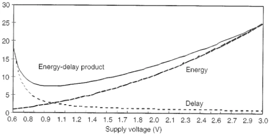
(25) P DP = Pav tp ,. (2.5). where Pav is the average power dissipation and tp is the propagation delay of the critical path. The PDP presents a measure of energy, as is apparent from the units (W x s = Joule). Here, the PDP is simply the average energy consumed per switching event.. 2.2.2. Energy-Delay Product. The scaling of Vdd is beneficial from the energy point of view but may have serious side effects on the delay. This means that using the energy as the metric is not sufficient. A more relevant metric has been proposed [18] as it accounts for both energy and delay by using the product of the energy per operation and the delay per operation. This metric can be used as the basis for design optimization and comparison between different systems. The energy-delay product (or EDP) is defined as EDP = P DP · tp = Pav t2p =. 2 CL VDD tp . 2. (2.6). It is important to observe the voltage dependence of the EDP. For low supply voltages, the energy is minimum but the delay is not. Increasing the supply voltage decreases the delay but at the expense of the energy as shown in Figure1 2.1. This indicates that an optimum operation point should exist as it can be determined from the energy-delay product.. 2.3. Power Reduction in CMOS Digital Circuits. The dominant term in modern circuits is the switching component, which suggests that reducing the supply voltage is the most effective way to decrease power consumption due to being a quadratic term. Other means for reducing switching power consumption include: reduction of the voltage swing in all the nodes, reduction of the switching probability, and reduction of the load capacitance. This thesis assumes that the power 1. Figure taken from [16].. 10.
(26) Figure 2.1: Energy-Delay Product consumption in CMOS is dominated by the dynamic power resulting from the charging and discharging of the capacitance 2 P = Ctotal VDD f,. (2.7). where Ctotal denotes the total capacitance of the circuit, VDD is the supply voltage, and f is the clock frequency of the circuit.. 2.3.1. Voltage Scaling. Reduction of the supply voltage is the key to achieving low-power operation since it plays an important role in the power dissipation of CMOS digital circuits as shown in Equation (2.7). However, when power supply reduction is implemented, several important issues must be addressed so that system performance is not sacrificed. One of these issues is the fact that since the core voltage is being reduced, the input and output signal levels of the circuit must be compatible with the peripheral circuitry, in order to maintain correct signal transmission. Thus, an important consideration is the increase of delay after a supply voltage reduction. A first-order approximation of the propagation delay tp is given by tp =. Ccrit VDD , k(VDD − Vt )2 11. (2.8).
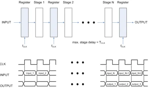
(27) where Ccrit denotes the capacitance to be charged/discharged in a single clock cycle, i.e., the capacitance of the critical path, VDD is the supply voltage, and Vt is the threshold voltage. The parameter k is a function of technology parameters µ,. W , L. and Cox .. For example, scaling the supply voltage from 5 to 3.3 V reduces the power dissipation by 56% with a propagation delay increase of 186%. For certain types of low-power applications this reduction in performance cannot be tolerated. Fortunately, there are architectural techniques to address this issue for systems where the throughput is more important than the speed. Parallel processing and pipelining are two of these techniques for lowering power consumption in systems where sample speed need not be increased [15]. 2.3.1.1. Parallel Processing for Low Power. The single functional block shown in Figure 2.2 illustrates the architectural techniques to reduce power consumption. Both the input and output vectors are sampled through register arrays, driven by a clock signal CLK. The critical path in this logic block (at a voltage supply of VDD ) allows a maximum sampling frequency of fCLK ; in other words, the propagation delay is equal to tp =. 1 . fCLK. One of these architectural techniques is parallel processing which can decrease the power consumption of a system by allowing the supply voltage to be reduced. In an Lparallel system, the charging capacitance does not change while the total capacitance is increased by L times (see Figure 2.3). In order to maintain the same rate, the clock period of the L-parallel circuit must be increased to LTorig , where Torig is the propagation delay of the original circuit given by Equation (2.8). This means that Ccrit is charged in time LTorig rather than in time Torig . In other words, there is more time to charge the same capacitance as shown in Figure 2.4. This idea can be utilized to reduce the supply voltage to βVDD [19]. The propagation delay of the original circuit is given by Equation (2.8) and the propagation delay of the L-parallel system is shown below LTorig =. Ccrit βVDD . k(βVDD − Vt )2. (2.9). Equating the propagation delays of both architectures, β can be obtained. Once β is 12.
(28) Figure 2.2: Single-stage implementation of a logic function calculated, the power consumption of the L-parallel system is given by using Equation (2.10).. 2 Ppar = (LCL )(βVDD ). f L. 2 = β 2 CL VDD f. = β 2 Porig. (2.10). where Porig is the power consumption of the original system given by Equation (2.7). The power consumption of the L-parallel system has been reduced by a factor of β 2 in comparison with the original system. However, this reduction comes at the expense of increased area—the replication of L times the logic of the original circuit plus the overhead of extra routing, resulting in a trade-off not suitable for area-constrained designs. 2.3.1.2. Pipelining for Low Power. Pipelining has been used to increase the sample speed of processing architectures [20]. In the case of low-power applications, speed is of second importance; therefore, pipelining can be used to maintain the throughput while reducing the supply voltage. 13.
(29) Figure 2.3: L-Parallel structure realizing the same logic function as in Figure 2.2 Consider an M -level pipelined system, where the critical path is reduced to. 1 M. of. its original length and the capacitance to be charged in a single clock cycle is reduced to. Ccrit M. (see Figure 2.5). It must be taken into account that the total capacitance of. the circuit does not change. If the frequency is kept constant, only a fraction of the original capacitance,. Ccrit , M. is being charged or discharged in the same amount of time. that was previously needed for the capacitance Ccrit (see Figure 2.6). This implies that the supply voltage can be reduced to βVDD , where β is a positive constant less than 1. The power consumption of the pipelined system will be 2 Ppip = CL β 2 VDD f = β 2 Pseq .. (2.11). Hence, the power consumption of the pipelined system has been reduced by a factor of β 2 when it is compared to the original system. After pipelining the filter, the capacitance of the critical path is reduced, and if we wanted to maintain the same throughput—by operating the pipelined circuit at the same clock rate as the original system— we can equate the propagation delay of both 14.
(30) Figure 2.4: Critical paths for original and 3-parallel systems architectures. The propagation delay of the pipelined filter is given by Tpip =. Ccrit βVDD M. k(βVDD − Vt )2. .. (2.12). Once β is obtained, the power consumption of the pipelined system can be calculated using Equation (2.11). The power savings achieved after using pipelining are comparable to those obtained after using parallel processing with the advantage of much lower area overhead. While the power reduction is significant, it should be noted that the supply voltage cannot be reduced indefinitely since it is lower bounded by the process parameters. It is worth mentioning that pipelining is a special case of cutset retiming; more specifically, pipelining applies to graphs without loops. For more information on retiming, the reader should consult [21], [19].. 2.3.2. Reduction of Switching Activity. The dynamic power consumption of CMOS digital circuits depends on the node transition factor α (also called switching activity factor). This factor is the effective number of power-consuming voltage transitions experienced by the output capacitance per clock cycle. This node transition factor depends on the Boolean function performed, the logic family, and the input signal statistics. Switching activity in CMOS digital circuits can be reduced by algorithmic optimization, by architecture optimization, by proper choice of logic topology, or by circuit-level optimization. Algorithmic optimization depends heavily on the application and on the characteristics of the data such as dynamic range, correlation, and statistics of data trans15.
(31) Figure 2.5: M-level pipelined structure realizing the function shown in Figure 2.2. Figure 2.6: Critical paths for original and 3-level pipelined systems mission. The representation of data can have a significant impact on switching activity at the system level. An example is the use of sign-magnitude representation instead of the conventional two’s complement representation for signed data. A change in sign will cause transition of the higher-order bits in the two’s complement representation, whereas only the sign bit will change in sign-magnitude representation. A different way to reduce switching activity is based on delay balancing and the reduction of glitches. In multi-level logic circuits, the propagation delay from one logic block to the next can cause spurious signal transitions, or glitches, as a result of critical races or dynamic hazards. If all input signals of a gate change simultaneously, no glitching occurs. A glitch can occur if input signals change at different times (see Figure 2.7). 16.
(32) Figure 2.7: Signal glitching in multi-level static CMOS digital circuits Another very effective design technique for reducing the switching activity in CMOS logic circuits is the use of conditional, or gated clock signals. This approach is used to put the circuits in a sleep mode when they are idle. If certain logic blocks in a system are not immediately used during the current clock cycle, temporarily disabling the clock signals of these blocks will save switching power that would be otherwise wasted (see Figure 2.8).. Figure 2.8: Gating signals Xi to enable clock to certain blocks on demand. 2.3.3. Reduction of Switched Capacitance. Energy consumption is proportional to switching capacitance. This capacitance can be broken into two categories, the capacitance in dense logic (which includes the transistor parasitic and wire capacitances at the output of the gates) and the capacitances of busses and a clock network (which is mainly wire capacitance). A comparison between the three logic families, static, dynamic, and the pass-gate (or CPL) [15] shows that the best logic family in terms of the energy required for a transition at a given amount of delay is the CPL. This comes at no surprise since 17.
(33) the CPL has the least transistor count for a given Boolean function implementation. This implies that the parasitic capacitances (gate oxide and source/drain diffusion capacitances) will be reduced. Therefore, CPL seems more attractive for low-power applications. Transistor sizing is imperative for speed and power. Conventional design strategies focus on speed. The delay specifications were satisfied by sizing the transistors. For low-power design, the rule is to size the transistors on the critical path only such that the speed requirements are met. The transistors on the noncritical paths should be kept at the least possible dimensions. The name of the game for low-power design is to use minimum-size transistor as much as possible [16].. 2.4. Pipelining Adaptive Digital Filters. As discussed earlier, pipelining is a helpful technique for lowering the supply voltage without decreasing throughput. It was also stated that pipelining is useful only for graphs without loops. Hence, pipelining of adaptive digital filters is an arduous task due to the presence of long feedback loops. Look-ahead transformation techniques [19] can be applied, but the resulting systems are not practical for hardware implementation [22]. Look-ahead transformations maintain the exact input-output behavior in frequency shaping filters, but in adaptive filter this input-output mapping is not that important since the coefficients continue to adapt until they converge. The relevant metrics in adaptive filtering are the misadjustment and the rate of convergence or adaptation time. The misadjustment provides a quantitative measure of the amount by which the final value of the mean-squared error (or MSE), averaged over an ensemble of adaptive filter, deviates from the minimum mean-squared error that is produced by the Wiener filter; in other words, the optimal solution [23]. The rate of convergence is defined as the number of iterations required for the algorithm, in response to stationary inputs, to converge “close enough” to the optimal solution. In this section, the relaxed-look ahead transformation technique [19] is presented to help in the pipelining of the adaptive filters with little of no increase in hardware at the expense of minimum degradation in the adaptation behavior. The relaxed-look ahead transformation is based on certain approximations of the look-ahead technique. There are three forms of relaxed-look ahead including product, sum, and delay. 18.
(34) 2.4.1. Relaxed Look-Ahead Techniques. Consider the 1st-order time-varying recursion given by y(n + 1) = a(n)y(n) + u(n). (2.13). with varying coefficients a(n). Using look-ahead, y(n + M) can be expressed in terms of y(n) as follows:. y(n + M ) = +. M −1 Y. a(n + M − 1 − i)y(n). i=0 M −1 i−1 Y X. [. a(n + M − 1 − j)]u(n + M − 1 − i). i=1 j=0. + u(n + M − 1).. (2.14). The computation structure corresponding to Equation (2.14) is shown in Figure 2.9 for M = 4. In general, the look-ahead transformation creates M − 1 extra delays in the recursive loop which can be used to pipeline the multiply-add operation in the loop. For example, the iteration period of the structure in Figure 2.9 is now limited by. Tm +Ta . 4. This transformation does not alter the input-output behavior. This has been achieved at the expense of the look-ahead overhead introduced by the 2nd term in the RHS of Equation (2.14), which is dependent on the level of pipelining M . Depending on the constraints, this overhead may be unacceptable. However, under certain circumstances we can substitute approximate expressions to simplify the terms in the RHS of Equation (2.14). This is referred to as relaxed-look ahead. 2.4.1.1. Product relaxation. If the magnitude of a(n) is close to unity, then a(n) can be replaced by (1 − ε(n)), where ε(n) is close to zero. Then we have the following approximation M −1 Y. a(n + 1) ≈ a(n + M − 1)M = (1 − ε(n + M − 1))M. i=0. = 1 − M ε(n + M − 1) = 1 − M (1 − a(n + M − 1)). 19. (2.15).
(35) Figure 2.9: A 4-level look-ahead pipelined 1st-order recursion. Furthermore, if u(n + i) is close to zero, then [. i−1 Y. a(n + M − 1 − j)]u(n + M − 1 − i). j=0. can be approximated as u(n + M − 1 − i).. Therefore, Equation (2.14) can be approximated as. y(n + M ) = (1 − M (1 − a(n + M − 1)))y(n) +. M −1 X. u(n + M − 1 − i).. (2.16). i=0. Hence, Equation (2.16) is the result of application of an M -level relaxed-look ahead with product relaxation to Equation (2.13). The computation structure corresponding to the 1st-order recursion in Equation (2.13) with 4-level product-relaxed pipelining is shown in Figure 2.10. Since a(n) is assumed to be close to 1, then. QM −1 j=0. a(n+M −1−j). can also be approximated as a(n + M − 1). Then another approximation of Equation (2.14) can be obtained as illustrated below 20.
(36) y(n + M ) = a(n + M − 1)y(n) +. M −1 X. u(n + M − 1 − i).. (2.17). i=0. Figure 2.10: A 4-level product-relaxed look-ahead pipelined 1st-order recursion. 2.4.1.2. Sum relaxation. If the input u(n) varies slowly over M cycles, then. PM −1 i=0. u(n + M − 1 − i) can be. approximated as M u(n). This leads to: y(n + M ) =. M −1 Y. a(n + M − 1 − i)y(n) + M u(n).. (2.18). i=0. If u(n) is also close to zero, then M u(n) can be approximated by u(n) to obtain y(n + M ) =. M −1 Y. a(n + M − 1 − i)y(n) + u(n).. (2.19). i=0. Thus, Equations (2.18) and (2.19) are the results of application of M -level relaxedlook ahead with sum relaxations to Equation (2.13). The computation structure of the 1st-order recursion with 4-levels of sum-relaxed pipelining is shown in Figure 2.11. 2.4.1.3. Delay relaxation. Consider the recursion 21.
(37) Figure 2.11: A 4-level sum-relaxed look-ahead pipelined 1st-order recursion. y(n) = y(n − 1) + a(n)u(n). (2.20). and its M -level look ahead pipelined version y(n) = y(n − M ) +. M −1 X. a(n − i)u(n − i).. (2.21). i=0. The delay relaxation involves the use of delayed input u(n−M 0 ) and delayed coefficient a(n − M 0 ) in Equation (2.21). This approximation is based on the assumption that the product a(n)u(n) is more or less constant over M 0 samples [24]. In general, this assumption is a reasonable approximation for stationary or slowly varying product a(n)u(n). Thus, Equation (2.21) is approximated as: y(n) = y(n − M ) +. M −1 X. a(n − M 0 − i)u(n − M 0 − i).. (2.22). i=0. These relaxed-look ahead techniques may be applied individually or in combination to derive different architectures. Each of these architectures will have its own behavior, which will depend upon the approximations made and their validity. The relaxed-look ahead is a transformation technique in the stochastic sense, since the average output profile maintained while the input-output behavior has been modified. 22.
(38) 2.5. A Survey of Power Optimization Techniques. A prediction made in 1965 by Gordon Moore, cofounder of Intel, stating that the number of transistors occupying a square inch of integrated circuit material would double each year since the invention of the integrated circuit has been maintained and still holds true today. This trend is expected to continue at least through the end of the decade. However, today’s researchers face the challenge of working within the physical limits of atomic structure for scaling transistors while managing both power and heat. Furthermore, frequency growth has dropped to 15 to 20 percent because of power limitations [25]. The challenge of the computer architecture community is to device innovative ways of delivering continuing growth in system performance while simultaneously solving the power problem. In response to these power and thermal challenges, researchers are aggressively delving into conventional and unconventional technologies. Instead of riding on the steady frequency progress of the past decade, improvements will be driven by integration at all levels in conjunction with hardwaresoftware optimizations. In this survey the focus is on the architectural and micro-architectural level of power optimization techniques. Topics like technology, logic, and system-level optimizations are beyond the scope of this paper.. 2.5.1. Memory Systems. From the earliest days of computing, researchers have wanted unlimited amounts of fast memory. This has been addressed in part by utilizing a memory hierarchy and with help from the fast pace of semiconductor technology, which has increased the level of integration exponentially with time. In today’s industry, the cost per memory bit is extremely low, and the amount of memory available is no longer the main issue. Now, the major topics regarding memory systems are related to performance and power consumption. The memory system consumes a significant amount of power of the total power consumption of microprocessors [26]. Memory systems have two sources of power loss. The first source is represented by the frequency of memory accesses; the second source is derived from the leakage current represented in the power equation. The on-chip L1 and L2 caches of the 21164 DEC Alpha chip dissipate 25% of the total power of the processor [27]. The StrongARM SA-110 processor from DEC, which targets specifically low-power applications, dissipates about 27% of the power in the 23.
(39) I-Cache [28]. In the Pentium Pro processor, the instruction fetch unit (IFU) and the I-Cache contribute 14% to the total power consumed [29]. The reason for the high-power consumption in the I-Cache subsystem is that the execution rate of a processor depends critically on the rate at which the instruction stream can be fetched from the I-Cache. The I-Cache should therefore be able to provide the data path of the machine with a continuous stream of instructions and has therefore very high switching activity. Bellas et al [30] are focusing on developing methods for reducing the energy dissipated in the on-chip caches since energy dissipated in caches represent a substantial portion in the energy budget of today’s processors. Furthermore, this portion is likely to increase in the near future. They propose a method that uses an additional minicache located between the I-Cache and the CPU core that buffers instructions that are nested within loops and are continuously otherwise fetched from the I-Cache. This mechanism is combined with code modifications, through the compiler, that greatly simplifies the required hardware, eliminates unnecessary instruction fetching, and consequently reduces the switching activity and the dissipated activity. Ko et al [31] present the characterization and design of energy efficient, on-chip cache memories. Their paper reveals that memory peripheral interface circuits and bit array dissipate comparable power; hence, to optimize performance and power in a processor’s cache, they propose a multidivided module (MDM) cache architecture to conserve energy in the bit array as well as the memory peripheral circuits. While the bulk of the power dissipated is dynamic switching power, leakage power is also beginning to be a concern. Chipmakers expect that in future chip generations, as feature sizes shrink, the dominant component of this power consumption will be leakage. Kaxiras, Hu, and Martonosi [32] examine methods for reducing leakage power within the cache memories of the CPU by discussing policies and implementations for reducing cache leakage by invalidating and “turning of” cache lines when they hold data not likely to be reused. A similar approach is examined in [26], where according to Kim et al, during a fixed period of time, the activity in a data cache is only centered on a small subset of the lines. This behavior can be exploited to cut the leakage power of large data caches by putting the cold cache lines into a state preserving, low-power drowsy mode. They investigate policies and circuit techniques for implementing drowsy data caches. In the case of embedded systems, one solution consists of mapping the most frequently accessed addresses onto the on-chip SRAM to guarantee power and performance 24.
(40) efficiency. This option is especially effective when memory access patterns can be profiled and studied at design time. Benini, Macii, and Poncino [33] propose an algorithm for the automatic partitioning of on-chip SRAM in multiple banks that can be independently accessed. By utilizing a dynamic execution profile of an embedded application running on a given processor core, they synthesize a multi-banked SRAM architecture optimally fitted to the execution profile. Su and Despain [34] present a case study of performance and power trade-offs in designing on-chip caches for the microprocessors used in portable computing applications.. 2.5.2. Buses. Interconnections heavily affect power consumption since it is the medium of most electrical activity. Buses are a significant source of power loss, especially interchip busses, which are often very wide. The standard PC memory bus includes 64 data lines and 32 address lines, and each line requires substantial drivers. A chip can expend 15% to 20% of its power on these interchip drivers [35]. According to Benini et al [36] the power dissipated by system-level busses is the largest contribution to the global power of complex VLSI circuits. Therefore, the minimization of the switching activity at the I/O interfaces can provide significant savings in the overall power budget. They present encoding techniques suitable for minimizing the switching activity of address buses by targeting the reduction of the average number of bus line transitions per clock cycle. In a similar manner, Aghaghiri et al [37] introduce an approach to decrease the switching activity of an address bus. They present a new address bus encoding technique. Their method is based on the limited weight encoding and transition signaling. The resulting code, ALBORZ, can be made adaptive to make the required encoder/decoder hardware smaller and achieve higher reduction in the switching activity. Kumar, Zyuban, and Tullsen [38] examine the area, power, performance, and design issues for the on-chip interconnects on a chip multiprocessor, attempting to present a comprehensive view of a class of interconnect architectures. Their paper shows that the design choices for the interconnections have significant effect on the rest of the chip, potentially consuming a significant fraction of the real estate and power budgets. To increase the level of integration and the performance, system-on-a-chip is widely 25.
(41) deployed in today’s designs. In such designs, communication resources are allocated to connect the on-chip modules for data exchange. Hsieh and Pedram [39] propose a splitbus architecture to improve the power dissipation for global data exchange among a set of modules. Their proposed split-bus architecture can be extended to multi-way split-bus when a large number of modules are to be connected.. 2.5.3. Processor. Chip-level design space includes two major options: how we trade power and performance within a single processor pipeline (core), and how we integrate multiple cores, accelerators, and off-load engines on chip to boost total chip-level performance [25]. In addition to fixing and scaling pipeline depth, additional enhancements to increase power efficiency at the microarchitectural level are possible. The computer architecture research community is exploring new architectures that are aware of power, energy, and thermal challenges and able to manage them dynamically while running applications. These architectures are described below and include multi-core microprocessors, clustered microarchitectures, and other power-optimized microarchitectures. With single-core performance improvements slowing, multiple cores per chip can help continue the exponential growth of chip-level performance. This solution exploits performance through higher chip, module, and system integration levels, and optimizes for performance through technology, system, software, and application sinergies [25]. Kumar et al [40] propose a single-ISA heterogeneous multi-core architecture as a mechanism to reduce processor power dissipation. They assume a single chip containing a diverse set of cores that target different performance levels and consume different levels of power. During an application’s execution, system software dynamically chooses the most appropriate core to meet specific performance and power requirements. Their initial results demonstrate a five-fold reduction in energy at a cost of only 25% performance. Several microprocessors, including Alpha 21264 and POWER4 use a compacting latch-based issue queue design which has the advantage of simplicity of design and verification. The disadvantage is its high power dissipation. Different issue queue power optimization techniques that vary not only in their performance and power characteristics, but in how much they deviate from the baseline implementation are explored in [41]. Li and Martı́nez [42] examine the power-performance implications of running parallel applications on chip multiprocessors (CMPs). They develop an analytical model 26.
(42) that puts together parallel efficiency, granularity of parallelism, and voltage/frequency scaling, to establish a formal connection with the power consumption and performance of a parallel code running on a CMP. Zyuban and Kogge’s work [43] attempts to bring the power issue to the earliest phases of microprocessor development. They investigate power-optimization techniques of superscalar microprocessors at the microarchitecture level by identifying major targets for power reduction. Then, they develop an energyefficient version of a multicluster microarchitecture that reduces energy in the identified critical design points with minimal performance impact.. Leakage power of execution units is a major concern in current and future microprocessor design. Hu et al [44] explore the potential of architectural techniques to reduce leakage through power-gating of execution units. Their paper focuses on hardware mechanisms, such as workload-driven, dynamic power-gating. They explain the microarchitecture and circuit-level design parameters that need to be considered in investigating the overall power savings potential in such an approach. Another paper that can be compared to this research is the one presented by Manne, Klauser, and Grunwald [29]. Their goal is to control speculation and reduce the amount of unnecessary work in high-performance, wide-issue, superscalar processors. They introduce a hardware mechanism called pipeline gating to control rampant speculation in the pipeline and present inexpensive mechanisms for determining when a branch is likely to mispredict, and for stopping wrong-path instructions from entering the pipeline; therefore, limiting speculation and reducing energy consumption. A different approach is the one presented by Srinivasan et al [45] where they introduce an optimization methodology that starts with an analytical power-performance model to derive optimal pipeline depth for a superscalar processor.. Recently, very long instruction word (VLIW) architectures have been proposed for high-performance embedded systems as an interesting alternative to more conventional CPUs, to balance performance with hardware complexity and scalability. An approach to the design of embedded VLIW processor architectures based on the forwarding (or bypassing) hardware, which provides operands from interstage pipeline registers directly to the inputs of the functions units is proposed in [46]. 27.
(43) 2.5.4. Dynamic Voltage Scaling. Dynamic frequency scaling (DFS) is a technique that seeks to reduce power consumption by changing the processor frequency based on the requirements of the executing application. For fixed-duration tasks, especially waiting, this usually results in a proportional reduction of energy use. For other tasks, because of the corresponding increases in execution time, DFS could either save or waste energy depending on second order effects. To guarantee energy savings, the processor voltage must be changed at the same time as the frequency. This technique is referred to as dynamic voltage-frequency scaling (DVFS), or as dynamic voltage scaling (DVS) [47]. There are many techniques that can be used to control the domain frequencies. Off-line algorithms may be best suited for applications which can be hand-tuned, which will exhibit run-time characteristics similar to the off-line analysis, and which are likely to repeat this behavior whenever they are executed. On-line algorithms may be best suited for situations where the applications that will be executed are not known or controllable. An on-line algorithm that reacts to the dynamic characteristics of the application to control domain frequencies is proposed in [48]. Hong et al [49] present a paper whose goal is to develop the design methodology for the low-power, core-based, real-time SOC based on dynamically variable voltage hardware. In their study they develop techniques that treat voltage as a variable to be determined, in addition to the conventional task scheduling and allocation. They also address the selection of the processor core and the determination of the instruction and data cache size and configuration so as to fully exploit dynamically variable voltage hardware. Flautner’s approach [50] is somewhat different. The aim of his performance-scaling technique is to take advantage of power-saving features on processors such as the Intel XScale and Transmeta Crusoe that allow the frequency of the processor to be reduced with proportional reduction in voltage. He uses episode-length information combined with a predictor as the basis for an automatic mechanism to estimate the optimum performance-level for program execution.. 2.5.5. Software. Software does not consume power, but the execution and storage of software requires energy consumption by the hardware. In this section we review some of the techniques used in different levels of software applications to reduce the power consumption at 28.
(44) diverse levels and on different components. Power optimization at the architectural and software levels has attracted the interest of a number of researchers. A model that views power from the standpoint of the software that executes on a microprocessor and the activity that it causes, rather than from the traditional hardware standpoint is proposed in [51]. A brief review of compiler techniques for power minimization is presented in [52] and [53]. The approach presented in [30] relies on profile data from previous runs to select the best instructions to be cached. The compiler maximizes the number of basic blocks that can be placed in the L-Cache by determining their nesting and using their execution profile. The resulting hardware is very simple and most of the task is carried out by the compiler; thus, reducing the power requirements of the extra cache. A different approach is given by [54] in which processor stalls can be used to increase the throughput by temporarily switching to a different thread of execution, or reduce the power and energy consumption by temporarily switching the processor to low-power mode. Shrivastava et al present code transformations to aggregate processor free time and use it to profitably switch the processor to low-power mode. Viswanath, Abraham, and Hunt [55] propose instruction-driven slicing, a technique for annotating microprocessor descriptions at the Register Transfer Level (RTL) in order to achieve lower power dissipation. The technique automatically annotates existing RTL code to optimize the circuit for lowering power dissipated by switching activity. Program code compression is an emerging research activity that is having an impact in several production areas such as networking and embedded systems. This is because the reduced-sized code can have a positive impact on network traffic and embedded system costs such as memory requirements and power consumption. A survey of code-size reduction methods is presented in [56].. 2.5.6. Power Management Techniques in the Industry. This section examines the power optimization and management techniques that the industry is currently adopting. The description of the low-power techniques utilized in three different processors, the Intel Pentium M, the Transmeta Efficeon, and the IBM Blue Gene, is discussed. The Pentium M carefully balances performance enhancing features with several powersaving features that increase the battery lifetime. It uses advanced power-aware 29.
(45) performance features including the innovative branch predictor, the dedicated stack manager, the micro-operation fusion, and the Intel Pentium M processor bus. To save energy, the Pentium M integrates several techniques that reduce the total switching activity, these include hardware for predicting idle units and inhibiting their clock signals, buses whose components are activated only when data needs to be transferred, and a technique called execution stacking which clusters units that perform similar functions into similar regions so that the processor can selectively activate the parts of the circuit that will be needed by an instruction. Also, the processor includes low leakage transistors in the caches. It supports an enhanced version of Intel’s SpeedStep technology that selfmanages voltage and frequency stepping [57]. Transmeta’s Efficeon processor saves power by means of its LongRun2 power manager. LongRun2 Technologies is a suite of advanced power management, leakage control and process compensation technologies that can diminish the negative effects of increasing leakage power and process variations in advanced nanoscale designs. This manager addresses these challenges with advanced algorithms, innovative circuits, process techniques, and software and manufacturing optimization methods. Further details are not known since they are proprietary. The Efficeon also saves power by shifting many of the complexities in instruction execution from hardware to software. The Efficeon relies on a code morphing software (CMS), a layer of software that reserves a small portion of main memory (typically 32 Mb) for its translation cache of dynamically translated x86 instructions into the processor’s native VLIW instructions. This reduces the on-chip area and its accompanying power dissipation [58]. Optimizing future supercomputing applications will depend on delivering the best performance for a given power budget. To deliver increasing aggregate performance for supercomputing workloads, the main challenge for today’s system engineers is addressing system power. For the Blue Gene/L system, a primary design constraint was power-performance efficiency in a high-density-computing system that would fit in the form factor of air-cooled racks in a standard machine room. The results on real-world applications from IBM’s engineers demonstrate that exploiting thread-level parallelism with lower-power cores offers significantly better power-performance characteristics than using higher-frequency cores with high power consumption. Additionally, exploiting data-level parallelism improves power-performance efficiency. The key to achieving application efficiency is to ensure good software parallelization efficiency [59]. 30.
(46) 2.5.7. Power-Performance Analysis Tools. Elevating power to a first-class constraint must be a priority early in the design stage when designers make architectural trade-offs as they perform cycle-accurate simulation. This presents a problem because designers can make accurate power determination only after they perform chip layout. However, designers can usually accept approximate values early in the design flow, provided they accurately reflect trends. For example, if the architecture changes, the approximate power figure should reflect a change in power in the correct direction [35]. Several research efforts are under way to insert power estimators into cycle-level simulators. Researchers at different locations [60],[61] have developed power estimators based on the SimpleScalar simulator. In [62] a complete system power simulator, called SoftWatt is presented. The tool models the CPU, memory hierarchy, and a low-power disk subsystem and quantifies the power behavior of both the application and operating system. The PowerTimer toolset [63] has been developed for use in early-stage microarchitecture-level power-performance analysis of microprocessors. The key component of the toolset is a parameterized set of energy functions that can be used in conjunction with any given cycle-accurate microarchitectural simulator. From the viewpoint of functional use, PowerTimer is similar to prior academic research tools such as Wattch [60], the most used research power-performance simulator within the academic community, and SimplePower [61]. In the embedded processors domain, there is SimBed [64], an execution-driven simulation testbed that measures the execution behavior and power consumption of embedded applications and RTOSs by executing them on an accurate architectural model of a microcontroller with simulated real-time stimuli. A simulator for memory systems is presented in [65]. The simulator is based on energy characterization of memory systems including buses, bus drivers, and memory devices by a cycle-accurate energy measurement technique.. 31.
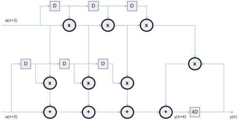
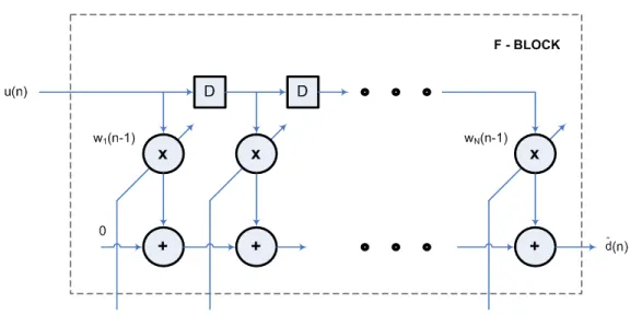
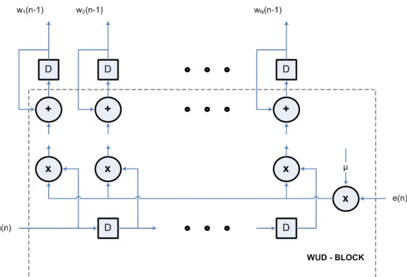
(47) Chapter 3 Filter Architecture 3.1. Introduction. Adaptive digital filters are successfully implemented in a variety of areas such as echo cancellation, adaptive control, voiceband modems, digital mobile radio, acoustic beamforming, channel equalization, and speech and image processing. The LMS algorithm is generally the most popular adaptation technique because of its simplicity and ease of computation. Different architectures of LMS adaptive filters can be considered depending on the primary design constraint whether it is area, performance, or power. This chapter discusses the design of the filter architecture. The first section gives an overview of the least-mean square algorithm, its basic components, and the equations that describe it. Section 3.3 introduces the adaptive noise canceling configuration for the adaptive filter. The following section offers the modeling of the input signals. In Section 3.5 we apply relaxed-look ahead transformation techniques to the original filter which allow us to pipeline the filter and give shape to the architecture. The final section presents the proposed architecture and a comparison between the original and the pipelined architectures.. 3.2. Least-Mean-Square Algorithm. This section is based on the book by Simon Haykin [23], and its intention is to introduce the reader into the fundamental concepts of adaptive filtering, specially, the least-meansquare algorithm. 32.
Figure
+7


Documento similar
The goal of this PhD thesis is to propose energy-aware control algorithms in EH powered vSCs for efficient utilization of harvested energy and lowering the grid energy consumption
While the product of the probability of the transit being in our light curve p o , with the signals of a given candidate having enough transit power (“energy”
According to Izquierdo (2008: 6), the nature of power and the interest of the agents for differential accumulation of power establish circular relations among the elites, because
As we have seen, even though the addition of a cosmological constant to Einstein’s eld equations may be the simplest way to obtain acceleration, it has its caveats. For this rea-
The rays within the same cluster have the same propagation delay, and the power dispersion of a clus- ter in angle domains is characterized by cluster angular spread of departure
In order to gain insight into the energy savings of µNap, we performed a complete state parametrisation (power consumption in transmission, reception, overhearing, idle and sleep)
In order to support energy savings for the AP, Wi-Fi Direct defines two new power saving mechanisms: the Opportunistic Power Save protocol and the Notice of Absence (NoA)
No obstante, como esta enfermedad afecta a cada persona de manera diferente, no todas las opciones de cuidado y tratamiento pueden ser apropiadas para cada individuo.. La forma
