Effect of the electrophoretic deposition of Au NPs in the performance CdS QDs sensitized solar cells
34
0
0
Texto completo
(2) 1 2 3 4 5 6 7 8 9 10 11 12 13 14 15 16 17 18 19 20 21 22 23 24 25 26 27 28 29 30 31 32 33 34 35 36 37 38 39 40 41 42 43 44 45 46 47 48 49 50 51 52 53 54 55 56 57 58 59 60 61 62 63 64 65. 1. Introduction The semiconductor Quantum Dots (QDs) have attract significant attention as possible candidates for increase the energy conversion efficiency in the solar cells, since their theoretical maximum efficiency is 44% QDs, e.g., CdSe, CdTe, CdS, PbS, PbSe, Bi2S3, and InP,[1-11] have been studied due to several advantage of the QDs, e.g.,have large extinction coefficients in the visible region and, after band gap excitation, undergo charge separation, injecting electrons to the conduction band of the metal oxide. QD-sensitized TiO2 solar cells have been reported to have quantum efficiency (QE) as high as 80%, [1-11] reaching photoconversion efficiencies (η) of 8%.[3,12]. Thus, for such a configuration, it is necessary to improve the electron injection efficiency to increase η and take advantage of the QDs strong photoabsorption in the visible spectrum. The photoresponse of semiconductors has also been improved with the presence of metallic NPs such as gold (Au) and silver (Ag), although the mechanism of the observed enhancement is not completely understood[3,5,13-20]. It has been suggested that such NPs enhance the visible-light-induced, electron-transfer process via Surface plasmon resonance.[3,21-28] However, mechanistic evidence that directly supports electron transfer arising from plasmon excitation remains elusive.[3,29,30] However, a strong increase in photoconversion efficiency with QD-sensitized Au-TiO2 NP composite have been found which was attributed to enhanced absorption of QDs caused by increased scattering of light by the Au NPs[13,17]. Other authors, had found that Au NPs act as electron traps to help separate the photogenerated charges and subsequently improve interfacial charge transfer[10,16,31-33]. Studies also have shown a shift in the Fermi level to a more negative. 2.
(3) 1 2 3 4 5 6 7 8 9 10 11 12 13 14 15 16 17 18 19 20 21 22 23 24 25 26 27 28 29 30 31 32 33 34 35 36 37 38 39 40 41 42 43 44 45 46 47 48 49 50 51 52 53 54 55 56 57 58 59 60 61 62 63 64 65. level (in respect to vacuum) by doping the semiconductor with metal NPs. This shift enhances the efficiency of the interfacial charge transfer process [1,10,16,18,31-36]. In this case a 40% improvement of hole transfer efficiency from the semiconductor film to the electrolyte has been reported[2,4,6,8-10,31,37-41].. One of the motivations in PV cell studies is to understand the processes involved in the charge carrier transport inside the cell.[1,3,5,7] The semiconductor/electrolyte interface extends to the entire film volume, implying that transport, reaction, and polarization processes occurring throughout the porous structure of the film are coupled in an intricate manner.[3,12] Electrochemical impedance spectroscopy (EIS) is an excellent and wellestablished technique for characterizing electrochemical systems, most notably for those involving a number of coupled processes.[3,5,13-20] EIS can identify important parameters affecting the cell performance, such as: (i) electron transport in the TiO2, which is influenced by the free carrier density and electron mobility, the latter being likely dependent on the carrier density, as the electron motion is a trap limited process,[3,2123,25-28] (ii) transfer of electrons to redox species in the electrolyte (sometimes named recombination or back reaction process in the context of DSSC studies), (iii) charging of the contact on the transparent conducting substrate (TCS) with the electrolyte (provided that the electrolyte penetrates the porous structure up to the substrate), and (iv) charging of capacitive elements in the high surface area porous structure, including the Helmholtz capacitance in the TiO2/electrolyte interface and the capacitances related to filling of the conduction band and surface states of the TiO2 in the porous structure.[3,29,30] In addition, the lifetime, the diffusion coefficient, and the diffusion length could be obtained[13,17]. In this work, we report a systematic characterization of CdS QDs sensitized TiO2 films 3.
(4) 1 2 3 4 5 6 7 8 9 10 11 12 13 14 15 16 17 18 19 20 21 22 23 24 25 26 27 28 29 30 31 32 33 34 35 36 37 38 39 40 41 42 43 44 45 46 47 48 49 50 51 52 53 54 55 56 57 58 59 60 61 62 63 64 65. decorated with Au NPs at different times of electrophoretic deposition. The objective is to improve the overall photoconversion efficiency by extracting more efficiently the electrons from the QDs with the help of Au NPs. A detailed study of the structural, optical, and photoelectrochemical properties was carried out to gain new insight into the underlying mechanism. Impedance analyses indicate that Au NPs deposited by this method affect at the same time two parameters, reducing the recombination processes and downshifting position of the TiO2’s CB, which result in an increase of the Voc, the electron transport and consequently the FF and .. 2. Experimental 2.1.. Preparation of TiO2 sensitized films. Materials. TiO2 Paste (WER2-0 Reflector) and TiO2 Paste (DSL 18NR-T) were obtained from DYESOL, Titanium (IV) isopropoxide (97%), Acetylacetone (>99%), Cadmium acetate dehydrate (Cd(CH3COO)2 2H2O), Zinc acetate dihydrate (Zn(CH3COO)2 2H2O) and Sodium hydroxide (NaOH) were obtained from Sigma-Aldrich. Sulphur (S), and Sodium sulphide (Na2S 9H2O) were obtained from KARAL and Fluorine-doped tin oxide (FTO) TEC-15 by MTI.. TiO2 film Preparation. Fluorine-doped tin oxide (FTO) glasses were cleaned with water, acetone and ethanol in an ultrasonic bath for 15 min each before use. All the photoelectrodes were made of three different TiO2 layers stacked one on the top of the other. 1) Compact layer: A solution of. 4.
(5) 1 2 3 4 5 6 7 8 9 10 11 12 13 14 15 16 17 18 19 20 21 22 23 24 25 26 27 28 29 30 31 32 33 34 35 36 37 38 39 40 41 42 43 44 45 46 47 48 49 50 51 52 53 54 55 56 57 58 59 60 61 62 63 64 65. titanium (IV) Isopropoxide (0.2M) in acetylacetone/ethanol (1:1 V:V) deposited by spray pyrolysis over an FTO and sintered at 450 °C for 30 min to obtain a 190 nm layer. This layer will avoid shortcuts reducing the recombination processes between the electrolyte and the FTO. 2) Transparent layer: TiO2 paste, (DSL 18-NRT, 20 nm average particle size) is deposited over the compact layer by Doctor Blade method obtaining a 6μm thick film. This layer will be the active layer i. e. where the sensitizers will be adsorbed and the mayor of the photo absorption process will be done. And 3) Scattering layer: a 9 µm layer is obtained by doctor blading depositing Wer2-O Reflector paste (400 nm particle size). This last layer will scatter the light that has passed through the first two layers without been absorbed, giving a second chance to be absorbed by the QDs. [4,11,42,43] The films were sintered for 30 min at 450 °C to obtain a good electrical contact between nanoparticles.. Au nanoparticles synthesis. The synthesis of Au NPs was based on the Turkevich method, by adding 3.75 ml of 1%wt. sodium citrate solution to a 0.001M HAuCl4 boiling solution and stirring at 500 rpm, until ruby red solution. Then the solution was cooled to room temperature and filtered. With this procedure13 nm particles were obtained. The size and shape were verified via UV-Vis absorption spectroscopy and TEM. Au deposit After synthesis, the Au NPs were deposited on the TiO2 films by electrophoresis. The samples were placed face to face with an FTO at distance of 0.2 cm and inserted in a cuvette with 2.5 mL of a colloidal suspension of the corresponding Au nanoparticles. Next, a 5V DC voltage was applied between the TiO2 films for several deposition times.. 5.
(6) 1 2 3 4 5 6 7 8 9 10 11 12 13 14 15 16 17 18 19 20 21 22 23 24 25 26 27 28 29 30 31 32 33 34 35 36 37 38 39 40 41 42 43 44 45 46 47 48 49 50 51 52 53 54 55 56 57 58 59 60 61 62 63 64 65. Film sensitization: The TiO2/Au Nps electrodes were in situ sensitized with CdS QDs grown by SILAR. For this purpose, solutions of 0.05M Cd(CH3COO)2 dissolved in ethanol as Cd2+ source and 0.05 M Na2S in methanol:water (V:V = 1:1) as S2- source, were used. A single SILAR cycle consisted of 1 min dip-coating the TiO2 electrode into the cadmium solution (Cd2+) and subsequently into the sulfide solutions, also during 1 min. After each dipping step in a precursor solution, the electrodes were thoroughly rinsed by immersion in the corresponding solvent in order to remove the excess of precursor. Seven SILAR cycles were done to obtain a uniform coverage of the TiO2 NPs with CdS QDs. To enhance the photovoltaic performance ZnS is deposited by SILAR for passivate CdS surface and reduce the recombination of electrons in the TiO2 to the polysulfide electrolyte [1,10,16,18,3133,35,36]. ZnS passivation was obtained by using 0.1M of Zn(CH3COO)2 2H2O and 0.1 M of Na2S both dissolved in water as Zn2+ and S2- sources respectively. The films were dipped for 1 min/dip in the solutions during 2 SILAR cycles.. Counter electrode manufacturing and assembling of solar cells: Cu2S counter electrodes were fabricated by immersing brass foil in an HCl solution (38% by volume) at 90 ºC for 1 hour. These substrates were sulfated by adding a drop of polysulfide electrolyte solution made by mixing solutions of Na2S (1 M), S (1.0 M), and NaOH (0.1 M) in distilled water. The solar cells were constructed by assembling the Cu2S counter electrode and the sensitized TiO2 film electrode with a binder clip separated by a scotch spacer. Lastly, a polysulfide electrolyte was introduced by dropping into the solar cell.. 6.
(7) 1 2 3 4 5 6 7 8 9 10 11 12 13 14 15 16 17 18 19 20 21 22 23 24 25 26 27 28 29 30 31 32 33 34 35 36 37 38 39 40 41 42 43 44 45 46 47 48 49 50 51 52 53 54 55 56 57 58 59 60 61 62 63 64 65. 2.2.. Characterization. Transmission Electron Microscopy (TEM) images were obtained from a FEI- Titan 80-300 KeV, microscope, equipped with ultra-stable Schottky field emitter gun. The UV-vis absorption spectra of the colloidal Au NPs were measured by transmittance and substrates were measured by diffuse reflectance in the range of 360 nm to 800 nm using an Agilent Technologies Cary Series UV-Vis-NIR spectrophotometer (Cary 5000) and an integrating sphere of 60 mm. The current density curves were measured with a reference 600 Gamry potensiotat, scanning from 0 to 600 mV at 100 mV/S. The samples were illuminated with an Oriel Sol 3A solar simulator while measuring. The light intensity was adjusted employing a NREL calibrated Si solar cell having KG-2 filter for one sun light intensity (100 mW/cm2). Best results are reported. IPCE spectra measurements were made with a monochromator (Newport model 74125). Electrochemical Impendance Spectroscopy (EIS) measurements were carried out by applying a small voltage perturbation (10 mV) at frequencies from 100 Hz to 0.1 Hz for different forward bias voltages in dark conditions.. 3. Results 3.1.. Structural and Morphological Characterization. Au Nanostructured particles The representative electron microscopy images from the gold nanostructured particles are shown in Figure 1. Nanospheres (NPs) have typically 12 nm of diameter and have good size confinement. 7.
(8) 1 2 3 4 5 6 7 8 9 10 11 12 13 14 15 16 17 18 19 20 21 22 23 24 25 26 27 28 29 30 31 32 33 34 35 36 37 38 39 40 41 42 43 44 45 46 47 48 49 50 51 52 53 54 55 56 57 58 59 60 61 62 63 64 65. TiO2 films In Figure 2 are presented SEM images of the transparent layer of the TiO2 films. It can be seen that when not decorated (Figure 2 a) the films are composed for 35nm average size TiO2 NPs agglomerated in a homogenous high porous arrangement. When Au NPs are electrophoretic deposited (see Figure 2 b), spherical particles of approximately 13 nm are observed on the film indifferently of the polarity applied to the sample during the deposit. The size and shape of the nanoparticles indicate that they are Au NPs. When the films are SILAR sensitized the TiO2 NPs are completely covered by the CdS QDs, partially filling the spaces between the particles. This gives the films a soft and less porous appearance (see Figure 2 c). Finally, when the films are decorated with Au NPs and sensitized with CdS to form TiO2/Au/CdS samples (Figure 2 d), a uniform coverage of the film with the QDs is obtained. But the appearance of the deposit is gnarled due to the presence of the Au NPs. EDS analyses of the films (Figure 2 e) confirm the presence of the Au NPs and Cd and S from the QDs.. Optical Absorption The absorption spectra of the Au NPs, bare TiO2 films, CdS QDs sensitized TiO2 films, 2.5 minutes Au NPs electrophoretic decorated films, Au decorated/ CdS QDs sensitized TiO2 films are shown in Figure 3. The Au NPs abortion (red circles) presents a well-defined peak at 519 nm that is consistent with the surface plasmon resonance (SPR) for such size of NPs. The TiO2 films (black solid line) have almost no absorption in the visible region, rapidly increasing for wavelengths ( ) lower than 400 nm. When Au NPs deposit is done for 2.5 min (orange +) there is a uniform increase in the absorption between 380 and 800 nm,. 8.
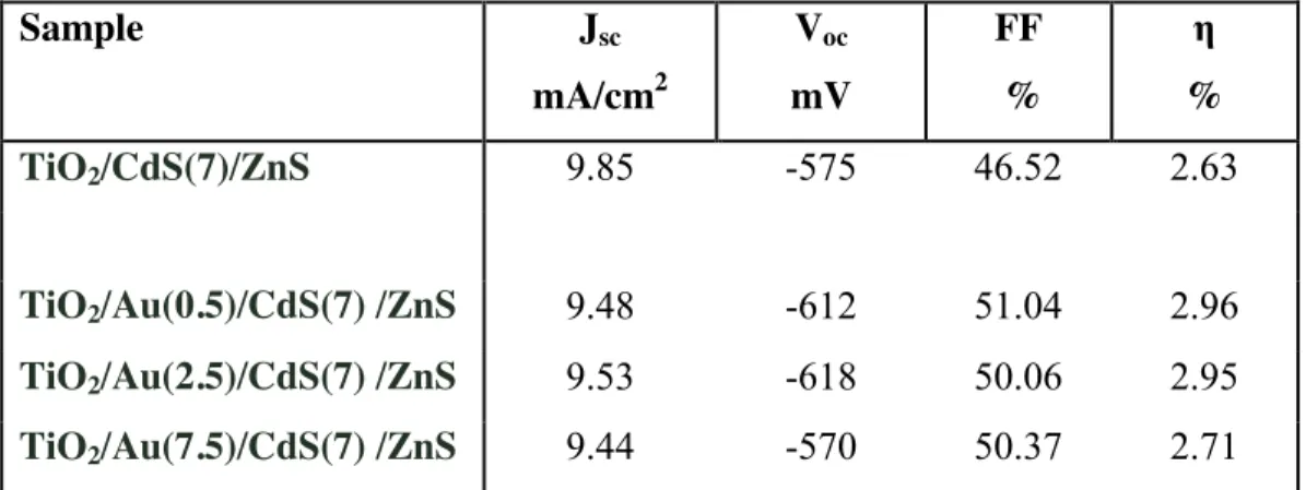
(9) 1 2 3 4 5 6 7 8 9 10 11 12 13 14 15 16 17 18 19 20 21 22 23 24 25 26 27 28 29 30 31 32 33 34 35 36 37 38 39 40 41 42 43 44 45 46 47 48 49 50 51 52 53 54 55 56 57 58 59 60 61 62 63 64 65. pointing to a light scattering effect. While, CdS sensitization of the TiO2 films (blue doted line) produces an absorption shoulder from 400 to 500 nm, which corresponds to the absorption of the CdS QDs[1,12,24,34]. Finally, when CdS sensitization is done in 2.5 min Au NPs decorated films, the shape in obtained spectra is similar to the films only sensitized with CdS QDs. But have a general increase in the absorption in the visible region, this increase match with the increase obtained in samples only decorated with Au NPs (orange +).. 3.2.. Photoelectrical Conversion Measurements. J-V Curves. Figure 4 shows the current density-voltage (J-V) profiles of the TiO2 films decorated by electrophoresis with Au NPs and further sensitized with CdS QDs (TiO2/Au/CdS) at several deposition times. Fill Factor (FF) and photoelectrical conversion efficiency (η) were calculated using Eq. 1 and Eq. 2 for short-circuit current density (Jsc) and open-circuit voltage (Voc) obtained from the curves[12-16,18,44,45]. 𝐹𝐹 =. 𝜂=. 𝑥100. 𝑥100 = 𝐹𝐹. (1). (2). where, Pm is the maximum power (J×V product) observed from the current density-voltage curve for each device and Pi is the incident light power density (100 mW×cm-2). Four. 9.
(10) 1 2 3 4 5 6 7 8 9 10 11 12 13 14 15 16 17 18 19 20 21 22 23 24 25 26 27 28 29 30 31 32 33 34 35 36 37 38 39 40 41 42 43 44 45 46 47 48 49 50 51 52 53 54 55 56 57 58 59 60 61 62 63 64 65. samples of each configuration were measured, finding a maximum relative standard deviation of 1.8%. Champion values are listed in Table 1. Analyzing the curves, it can be seen than the TiO2/CdS films (black line), have a Jsc of 9.85 mA/cm2 an Voc of 575 mV, a FF of 46.5% and a photoconversion efficiency of 2.63%, which is in good agreement with the efficiencies reported for this kind of solar cells[13,14,16,18,46-49]. When a 30s Au NPs deposit is applied (TiO2/Au(0.5)/CdS), a small reduction in the photocurrent is obtained (Jsc 9.5 mA) maintaining relatively constant for longer deposition times (9.5 and 9.4 mA for 2.5 and 7.5 min respectively). At the same time, the Au NPs deposit increases the Voc to 612 mV at 30 seconds of deposit. Maintaining almost constant for 2.5 min of deposit (618 mV) and reducing for higher times (570 mV for 7.5 min). In a similar way, the Au NPs deposit increases the FF to 51.0% with the first 30 seconds of electrophoresis, and maintaining almost constant for higher deposition times (50 and 50.3 for 2.5 and 7.5 min respectively). Finally, to test the deposition order effect, TiO2/CdS/Au samples were made. Inset in Figure 4 shows the champion cells of each configuration (TiO2/CdS ,TiO2/CdS/Au and TiO2 /Au/CdS). It can be seen that Au NPs addition after CdS sensitization result in a general reduction of the cell performance, possibly due to a partial removing or damage of the QDs.. IPCE Characterization Jsc is mainly dominated by two phenomena, the photogeneration (i.e. the process where photons are absorbed to generate electron hole pairs) and the injection (the transference of the electrons and holes from the photogenerator to the electron and hole transporter respectively). To understand the photogeneration in terms of the contribution of each. 10.
(11) 1 2 3 4 5 6 7 8 9 10 11 12 13 14 15 16 17 18 19 20 21 22 23 24 25 26 27 28 29 30 31 32 33 34 35 36 37 38 39 40 41 42 43 44 45 46 47 48 49 50 51 52 53 54 55 56 57 58 59 60 61 62 63 64 65. wavelength, the incident photon to current conversion efficiency (IPCE), A.K.A.external quantum efficiency (QE), was calculated by was calculated by the expression.. 𝐼𝑃𝐶𝐸(%) =. ( (. ). / (. ) /. ). 𝑥 100. (3),. Where Pinc stand for the light incident power. Figure 5 shows the IPCE curves TiO2/Au/CdS samples. Here it can be appreciated that samples without Au NPs have a QE higher than 60% in the 380-530nm, reaching it maximum at 460 nm (QE=72%) and rapidly decreasing for >550 nm.With 0.5 min of Au NPs deposit (green line) a reduction in the QE in the 380-530 nm region is obtained with an small increase over a wide range of wavelengths between 550 and 700 nm, when the deposition time is increased to 2.5 min (blue line) it is obtained almost the same spectrum than for 0.5 min but without the contribution in the 550 to 700 nm. With higher deposition times (7.5 min, pink line) a stronger reduction of QE are observed. These reductions in the QE are consistent with the reductions in Jsc. These results in conjunction with the absorbance curves indicate that a small coverage with Au NPs could increase the photoabsorption of the CdS or electron injection into the mesoscopic TiO2 due to the good conductivity of Au NPs. While for higher coverage Au NPs act as an optical filter reducing the amount of light reaching the absorbing elements (TiO2 and QDs).. Electrochemical Impedance Electrochemical impedance spectroscopy (EIS) measurements were carried out to explain the trends observed in the solar cell parameters (particularly Voc and FF) in terms of. 11.
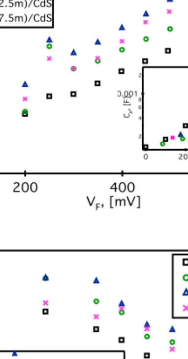
(12) 1 2 3 4 5 6 7 8 9 10 11 12 13 14 15 16 17 18 19 20 21 22 23 24 25 26 27 28 29 30 31 32 33 34 35 36 37 38 39 40 41 42 43 44 45 46 47 48 49 50 51 52 53 54 55 56 57 58 59 60 61 62 63 64 65. the internal physical processes when Au Nanoparticles are deposited. To do appropriate fit the EIS measurements, the equivalent circuit shown in Figure 6 was used [5,21,23,24,26,50-52] Where Rs is the series resistance and is related to the resistance of FTO and the wires resistance, Rcon and Ccon are the resistance and capacitance associated to the charge transfer in the counter electrode, Rt (=rt/L) is the transport resistance, and is related with the resistance to the electron flux inside of TiO2/sensitizer composite, which include the electron transport inside of the nanostructured particles, and between the nanostructured particles. Rrec (=rrec/L) and Cµ (=cµ L) are the charge transfer resistance and the chemical capacitance respectively. Where Rrec is inversely proportional to the recombination rate. These last three mentioned elements are denoted in lowercase. letters in figure 6 meaning the element per unit length for a film of thickness L, because they are distributed in a repetitive arrangement of a transmission line. Cµ , Rrec and Rt extracted from the EIS fitting of the CdS and Au/CdS sensitized solar cells are shown in Figure 7. Cµ is represented versus the applied voltage (Vapp) less the voltage drop due to FTO and wire resistance at the photoanode (Vseries=RsxJ). Then the new voltage is defined as Vf=Vapp-Vseries [29,50,53,54]. The chemical capacitance is proportional to the density of states (DOS) in the band gap, DOS increases exponentially with the proximity to the conduction band (CB), then, an increase in Cµ suggest a displacement to lower energies of the TiO2 CB. Rrec and Rt are exponentially dependent on carrier density (i.e. the distance to CB), then, to correctly evaluate this parameters a new potential is defined where, the measurements are at the same equivalent value of position to the CB of each device, using the equation [13,54]. 𝑉. = 𝑉 − Δ𝑉. (4),. 12.
(13) 1 2 3 4 5 6 7 8 9 10 11 12 13 14 15 16 17 18 19 20 21 22 23 24 25 26 27 28 29 30 31 32 33 34 35 36 37 38 39 40 41 42 43 44 45 46 47 48 49 50 51 52 53 54 55 56 57 58 59 60 61 62 63 64 65. Where ecb means equivalent conduction band and Δ𝑉 is the voltage shift observed between the Au decorated samples and the CdS sensitized film in Figure 7 a. After the voltage correction Cµ overlaps as shown in the inset of Figure 7 omparing Rrec and Cµ for the cells, it is viable to understand the origin in the Voc variation. [10,16,31-33,50]. Higher Voc observed in Au decorated cells could be due to three processes: (1) An increase in the absorption. (2) A shift in the TiO2 CB, and/ or (3) a change in the recombination rate. An increase in the photo absorption will result in an increase in Jsc and Voc. As previously discussed the photoabsorption in these samples is reduced. Then, hypothesis 1 can be discarded The second effect, a shift in the TiO2 CB, produces a movement of the TiO2 electron quasi-Fermi level, which determines the Voc, then an upward of the TiO2 CB will mean an increase in the Voc. This upward displacement of the conduction band is identified, by a shift to higher potentials of Cµ (i.e. a reduction of the capacitance). When Au are deposited, a general increase in Cµ is observed (see Figure 7 a) which means a downshift in the conduction band and the Voc. It is observed that for short depositions times (0.5 min) a downshift of about 85 mV is obtained (green circles), when the deposition time is increased to 2.5 min the band shift increases to approximately 175 mV (blue triangles). Finally, for higher deposition times, a reduction in the shift is obtained (135 mV at 7.5 min). These results as the obtained for Jsc contravene the observed Voc behavior of such samples, indicating that the photocurrent is not the dominant process in the Voc variations. The third effect, the recombination rate, can be also determined with EIS by analyzing the Rrec. Where an increase in this parameter indicates a reduction in the electron recombination processes from the TiO2 CB to acceptor states either in the electrolyte or the sensitizer[34,54]. Comparing TiO2/Au/CdS and TiO2/CdS samples in Figure 7b, it is 13.
(14) 1 2 3 4 5 6 7 8 9 10 11 12 13 14 15 16 17 18 19 20 21 22 23 24 25 26 27 28 29 30 31 32 33 34 35 36 37 38 39 40 41 42 43 44 45 46 47 48 49 50 51 52 53 54 55 56 57 58 59 60 61 62 63 64 65. observed that with 0.5 min of deposit Rrec increases (green circles), indicating an increase of the Voc. When the deposition time is increased to 2.5 min a higher increase in R rec is obtained (blue triangles). If the deposition time still increasing (7.5 min) Rrec have a small reduction, resulting in a resistance a little lower than the obtained for the samples with 0.5 min of deposit. Analyzing these same results in the Vecb convention, it is observed that with the first 30 seconds of Au NPs deposit the increase in Rrec is stronger than the observed in the Vf convention, and when the deposition time is increased to 2.5 min still increasing, while for 7.5 min of Au NPs deposit Rrec drops until reach the resistance obtained for 0.5 min of deposit. These results imply that the observed increases in Rrec in the Vf convention are the result of strong reductions in the recombination processes (possibly due to a passivation of the TiO2 superficial defects) that are slightly masked by the TiO2’s CB displacement. Then, when Au NPs are deposited, two simultaneous processes affect the Voc. On one side the TiO2 CB is downshifted reducing the Voc, but at the same time Recombination processes are considerably reduced upshifting the Fermi level and the Voc. At the end the reduction of recombination processes overcome the effect of the CB shift increasing the photovoltage. Another important parameter that is positively affected by the Au deposit is the FF. Variations in this parameter can be due to changes in the Transport resistance (Rt), where a reduction in Rt results in a FF increment [2,4,6,8-10,31,37-41,50]. The Rt behavior in the samples (Figure 7 c) indicate that for 30 seconds of Au NPs deposit (green circles) slightly reduces Rt, with the increase in the deposition time Rt increases until the 7.5 minutes deposit, when Rt reaches the same level than samples without Au NPs deposit indicating an increase in the electron transport (and the FF) with the first 30s of Au NPs deposit and an 14.
(15) 1 2 3 4 5 6 7 8 9 10 11 12 13 14 15 16 17 18 19 20 21 22 23 24 25 26 27 28 29 30 31 32 33 34 35 36 37 38 39 40 41 42 43 44 45 46 47 48 49 50 51 52 53 54 55 56 57 58 59 60 61 62 63 64 65. slow reduction of these parameter with higher deposition times, which match with the behavior observed in table 1. Analyzing these curves in the Vecb convention (inset of Figure 7 c) it could be appreciated than the Au deposit increases the resistance to the electron flux, this suggest that Au NPs pore filling is hindering the movement of the electrolyte ions affecting the electron motion in the TiO2. However, the CB shift produces an effective increase in the electron flux that overcompensates the Au NPs pore filling effect resulting in the increase of the FF.. 4. Discussion In summary, when a photon of visible light ( = 370-570 nm) insides on the CdS QDs of TiO2/CdS samples, an electron hole pair is generated (see Figure 8 a), the electron is injected from the CdS QD’s CB to the TiO2’s CB driven by the energy difference between the bands. , then it will be transported by the TiO2 and in an ideal case to the FTO and the. electrical circuit. However, some electrons interact whit trap levels in the QD/TiO2, giving a recombination process (red arrow in Figure 8 a ) reducing the performance of the cell. In the other side, holes are taken by the electrolyte via the oxidation of the 𝑆 shown in the Figure 8a. After that, the resulting 𝑆 electrode where they are reduced to 𝑆. ions, as. ions moved by diffusion to the counter. ions and the circuit is closed. As previously. discussed, in these conditions Jsc is principally determined by the photogeneration process (the amount of photons that inside in the QDs and the efficiency to convert such photons in electron hole pairs), and the injection process (driven by. ). Meanwhile, the Voc is due to. the energy difference between the Fermi level of the TiO2 (EF) and the redox level. Finally, the FF will be determined by the ratio of the transport and recombination processes.. 15.
(16) 1 2 3 4 5 6 7 8 9 10 11 12 13 14 15 16 17 18 19 20 21 22 23 24 25 26 27 28 29 30 31 32 33 34 35 36 37 38 39 40 41 42 43 44 45 46 47 48 49 50 51 52 53 54 55 56 57 58 59 60 61 62 63 64 65. When Au NPs are deposited various simultaneous processes occurred (Figure 8 b). (1) Au NPs act as an optical filter, reducing the amount of light that reaches the CdS QDs, which will result in a reduction of Jsc. (2) The TiO2 CB is downshifted by the energy levels equilibration process. This band movement will affect at the same time three parameters, Jsc is slightly increased by the increase in the potential energy between the sensitizer and the TiO2 (∆ ), Voc is reduced by the downshift of EF, and the FF is considerable increased by a reduction in the transport resistance. (3) The recombination processes are considerably reduced, resulting in higher amount of electrons in the TiO2’s CB; this upshifts EF and increments Voc. Then, when these three processes are combined in the right proportion what is obtained is a reduction in Jsc, an increase in Voc and an increase in FF that together give an increase in the photoconversion efficiency from 2.6 to 2.9%.. 5. Conclusions. The photovoltaic properties of CdS QD-sensitized TiO2 NC films decorated by electrophoresis with Au NPs at different deposition times have been systematically studied and analyzed. It was demonstrated that Au NPs could improve the photoconversion efficiency of TiO2/CdS QDs films when applied very short deposition times (30 seconds), by increasing Voc and FF sacrificing Jsc. IPCE measurements show that the presence of Au NPs reduces the capacity of the CdS QDs to absorb light, and impedance spectroscopy analyses indicates that Au NPs at the same time moves down the TiO2’s CB and reduces the recombination processes. The band movement helps to reduce the photocurrent losses. 16.
(17) 1 2 3 4 5 6 7 8 9 10 11 12 13 14 15 16 17 18 19 20 21 22 23 24 25 26 27 28 29 30 31 32 33 34 35 36 37 38 39 40 41 42 43 44 45 46 47 48 49 50 51 52 53 54 55 56 57 58 59 60 61 62 63 64 65. due to the absorption issue, and the reduction in the recombination processes give the observed increase in Voc (from 575 to 611 mV) and FF (from 46 to 50 %), that result in the final increase in. from 2.6 to 2.9 % .. Acknowledgments: We acknowledge financial support from CONACYT through grant 134111, the UCMEXUS program grant 00007, the European Community Seven Framework Program (FP7428 NMP-2010-EU-MEXICO), CIO-UGTO 2013 y 2014 and the CEMIE-Solar (04002) consortium. D. Esparza, and eja acknowledge scholarship from CONACYT and thanks to Maria Christian Albor for SEM and EDS analysis. Isaac Zarazúa thanks to CONACYT for the postdoctoral fellow.. 17.
(18) 1 2 3 4 5 6 7 8 9 10 11 12 13 14 15 16 17 18 19 20 21 22 23 24 25 26 27 28 29 30 31 32 33 34 35 36 37 38 39 40 41 42 43 44 45 46 47 48 49 50 51 52 53 54 55 56 57 58 59 60 61 62 63 64 65. References. [1]. V. González-Pedro, C. Sima, G. Marzari, P.P. Boix, S. Giménez, Q. Shen, et al., High performance PbS Quantum Dot Sensitized Solar Cells exceeding 4% efficiency: the role of metal precursors in the electron injection and charge separation, Phys. Chem. Chem. Phys. 15 (2013) 13835. doi:10.1039/c3cp51651b.. [2]. A. Kongkanand, K. Tvrdy, K. Takechi, M. Kuno, P.V. Kamat, Quantum Dot Solar Cells. Tuning Photoresponse through Size and Shape Control of CdSe-TiO2 Architecture, J. Am. Chem. Soc. 130 (2008) 4007–4015.. [3]. F. Fabregat-Santiago, G. Garcia-Belmonte, J. Bisquert, A. Zaban, P. Salvador, Decoupling of Transport, Charge Storage, and Interfacial Charge Transfer in the Nanocrystalline TiO 2/Electrolyte System by Impedance Methods, J. Phys. Chem. B. 106 (2002) 334–339. doi:10.1021/jp0119429.. [4]. I. Mora-Seró, T. Dittrich, A. Susha, A. Rogach, J. Bisquert, Large improvement of electron extraction from CdSe quantum dots into a TiO2 thin layer by N3 dye coabsorption, Thin Solid Films. 516 (2008) 6994–6998.. [5]. F. Fabregat-Santiago, J. Bisquert, G. Garcia-Belmonte, G. Boschloo, A. Hagfeldt, Influence of electrolyte in transport and recombination in dye-sensitized solar cells studied by impedance spectroscopy, Sol. Energy Mater. Sol. Cells. 87 (2005) 117– 131. doi:10.1016/j.solmat.2004.07.017.. [6]. T. Lopez-Luke, A. Wolcott, L. Xu, S. Chen, Z. Wen, J. Li, et al., Nitrogen-doped and CdSe quantum-dot-sensitized nanocrystalline TiO2 films for solar energy conversion applications, J. Phys. Chem. C. 112 (2008) 1282–1292.. [7]. P.P. Boix, G. Larramona, A. Jacob, B. Delatouche, I. Mora-Sero, J. Bisquert, Hole Transport and Recombination in All-Solid Sb 2S 3-Sensitized TiO 2Solar Cells Using CuSCN As Hole Transporter, J. Phys. Chem. C. 116 (2012) 1579–1587. doi:10.1021/jp210002c.. [8]. T. Zeng, S. Liu, F. Hsu, K. Huang, H. Liao, Effects of bifunctional linker on the performance of P3HT/CdSe quantum dot-linker-ZnO nanocolumn photovoltaic 18.
(19) 1 2 3 4 5 6 7 8 9 10 11 12 13 14 15 16 17 18 19 20 21 22 23 24 25 26 27 28 29 30 31 32 33 34 35 36 37 38 39 40 41 42 43 44 45 46 47 48 49 50 51 52 53 54 55 56 57 58 59 60 61 62 63 64 65. device, Opt. Express. 18 (2010) 130137. [9]. A. Franceschetti, J. An, A. Zunger, Impact ionization can explain carrier multiplication in PbSe quantum dots, Nano. Lett. 6 (2006) 2191–2195.. [10]. I. Zarazúa, E. De La Rosa, T. Lopez-Luke, J. Reyes-Gomez, S. Ruiz, C. Angeles Chavez, et al., Photovoltaic Conversion Enhancement of CdSe Quantum DotSensitized TiO2 Decorated with Au Nanoparticles and P3OT, J. Phys. Chem. C. 115 (2011) 23209–23220.. [11]. D. Esparza, I. Zarazúa, T. Lopez-Luke, R. Carriles, Photovoltaic Properties of Bi2S3 and CdS Quantum Dot Sensitized TiO2 Solar Cells, Electrochimical Acta. (2015) 486–492.. [12]. C. Chuang, P.R. Brown, V. Bulović, M.G. Bawendi, Improved performance and stability in quantum dot solar cells through band alignment engineering : Nature Materials : Nature Publishing Group, Nature Mater. (2014).. [13]. L. Liu, G. Wang, Y. Li, Y. Li, J.Z. Zhang, CdSe quantum dot-sensitized Au/TiO2 hybrid mesoporous films and their enhanced photoelectrochemical performance, Nano Research. (2011) 1–10.. [14]. G. Zhao, H. Kozuka, T. Yoko, Photoelectrochemical properties of dye-sensitized TiO2 films containing dispersed gold metal particles prepared by sol-gel method, Nippon Seramikkusu Kyokai Gakujutsu Ronbunshi. 104 (1996) 164–168.. [15]. Y. Nakato, M. Shioji, H. Tsubomura, Photoeffects on the potentials of thin metal films on a n-TiO2 crystal wafer. The mechanism of semiconductor photocatalysts, Chem. Phys. Lett. 90 (1982) 453–456. doi:10.1016/0009-2614(82)80253-4.. [16]. N.. Chandrasekharan,. P.V.. Kamat,. Improving. the. Photoelectrochemical. Performance of Nanostructured TiO2 Films by Adsorption of Gold Nanoparticles†, J. Phys. Chem. B. 104 (2000) 10851. [17]. C. He, Z. Zheng, H. Tang, L. Zhao, Electrochemical impedance spectroscopy characterization of electron transport and recombination in ZnO nanorod dyesensitized solar cells, J. Phys. Chem. C. 113 (2009) 10322–10325.. [18]. Y. Tian, T. Tatsuma, Mechanisms and Applications of Plasmon-Induced Charge Separation at TiO2 Films Loaded with Gold Nanoparticles, J. Am. Chem. Soc. 127 (2005) 7632–7637. doi:10.1021/ja042192u.. 19.
(20) 1 2 3 4 5 6 7 8 9 10 11 12 13 14 15 16 17 18 19 20 21 22 23 24 25 26 27 28 29 30 31 32 33 34 35 36 37 38 39 40 41 42 43 44 45 46 47 48 49 50 51 52 53 54 55 56 57 58 59 60 61 62 63 64 65. [19]. Y.Y. Proskuryakov, K. Durose, M.K. Al Turkestani, I. Mora-Seró, G. GarciaBelmonte, F. Fabregat-Santiago, et al., Impedance spectroscopy of thin-film CdTe/CdS solar cells under varied illumination, J. Appl. Phys. 106 (2009) 044507. doi:10.1063/1.3204484.. [20]. I. Mora-Sero, Y. Luo, G. Garcia-Belmonte, J. Bisquert, D. Muñoz, C. Voz, et al., Recombination rates in heterojunction silicon solar cells analyzed by impedance spectroscopy at forward bias and under illumination, Sol. Energy Mater. Sol. Cells. 92 (2008) 505–509. doi:10.1016/j.solmat.2007.11.005.. [21]. A. Liu, Q. Ren, M. Zhao, T. Xu, M. Yuan, T. Zhao, Photovoltaic performance enhancement of CdS quantum dot-sensitized TiO2 photoanodes with plasmonic gold nanoparticles, Journal of Alloys and …. (2014).. [22]. P. de Jongh, D. Vanmaekelbergh, Trap-Limited Electronic Transport in Assemblies of Nanometer-Size TiO2 Particles, Phys. Rev. Lett. 77 (1996) 3427–3430. doi:10.1103/PhysRevLett.77.3427.. [23]. W.-L. Liu, F.-C. Lin, Y.-C. Yang, C.-H. Huang, S. Gwo, M.H. Huang, et al., Influence of morphology on the plasmonic enhancement effect of Au@TiO2 coreshell nanoparticles in dye-sensitized solar cells, arXiv. cond-mat.mtrl-sci (2013).. [24]. P.N. Kumar, R. Narayanan, M. Deepa, A.K. Srivastava, Au@poly(acrylic acid) plasmons and C60 improve the light harvesting capability of a TiO2/CdS/CdSeS photoanode, J. Mater. Chem. A. 2 (2014) 9771. doi:10.1039/c4ta01140f.. [25]. R. Könenkamp, R. Henninger, Recombination in nanophase TiO2 films, Applied Physics A. 58 (1994) 87–90.. [26]. Y. Nishijima, K. Ueno, Y. Yokota, Plasmon-Assisted Photocurrent Generation from Visible to Near-Infrared Wavelength Using a Au-Nanorods/TiO2 Electrode, J. Phys. Chem. Lett. (2010).. [27]. R. Könenkamp, Carrier transport in nanoporous TiO2 films, Phys. Rev. B. 61 (2000) 11057–11064. doi:10.1103/PhysRevB.61.11057.. [28]. J. van de Lagemaat, A.J. Frank, Effect of the Surface-State Distribution on Electron Transport in Dye-Sensitized TiO 2Solar Cells: Nonlinear ElectronTransport. Kinetics,. J.. Phys.. Chem.. B.. 104. (2000). 4292–4294.. doi:10.1021/jp000836o.. 20.
(21) 1 2 3 4 5 6 7 8 9 10 11 12 13 14 15 16 17 18 19 20 21 22 23 24 25 26 27 28 29 30 31 32 33 34 35 36 37 38 39 40 41 42 43 44 45 46 47 48 49 50 51 52 53 54 55 56 57 58 59 60 61 62 63 64 65. [29]. Y.-S. Chen, H. Choi, P.V. Kamat, Metal-Cluster-Sensitized Solar Cells. A New Class of Thiolated Gold Sensitizers Delivering Efficiency Greater Than 2%, J. Am. Chem. Soc. 135 (2013) 8822–8825. doi:10.1021/ja403807f.. [30]. G. Franco, J. Gehring, L.M. Peter, E.A. Ponomarev, I. Uhlendorf, FrequencyResolved Optical Detection of Photoinjected Electrons in Dye-Sensitized Nanocrystalline Photovoltaic Cells, J. Phys. Chem. B. 103 (1999) 692–698. doi:10.1021/jp984060r.. [31]. A. Dawson, P.V. Kamat, Semiconductor− Metal Nanocomposites. Photoinduced Fusion and Photocatalysis of Gold-Capped TiO2 (TiO2/Gold) Nanoparticles, J. Phys. Chem. B. (2001).. [32]. V. Subramanian, E. Wolf, P.V. Kamat, Semiconductor-Metal Composite Nanostructures. To What Extent Do Metal Nanoparticles Improve the Photocatalytic Activity of TiO2 Films? J. Phys. Chem. B. 105 (2001) 11439–11446.. [33]. I. Zarazúa, T. Lopez-Luke, J. Reyes-Gomez, A. Torres Castro, J.Z. Zhang, E. De la Rosa, Impedance Analysis of CdSe Quantum Dot-Sensitized TiO2 Solar Cells Decorated with Au Nanoparticles and P3OT, Journal of the Electrochemical Society. (2014).. [34]. G. Burgeth, H. Kisch, Photocatalytic and photoelectrochemical properties of titania–chloroplatinate(IV), Coordination Chemistry Reviews. 230 (2002) 41–47. doi:10.1016/S0010-8545(02)00095-4.. [35]. I. Mora-Sero, S. Giménez, F. Fabregat-Santiago, R. Gomez, Q. Shen, T. Toyoda, et al., Recombination in Quantum Dot Sensitized Solar Cells, Acc. Chem. Res. 42 (2009) 1848–1857. doi:10.1021/ar900134d.. [36]. N. Guijarro, J.M. Campiña, Q. Shen, T. Toyoda, T. Lana-Villarreal, R. Gomez, Uncovering the role of the ZnS treatment in the performance of quantum dot sensitized. solar. cells,. Phys.. Chem.. Chem.. Phys.. 13. (2011). 12024.. doi:10.1039/c1cp20290a. [37]. I. Robel, V. Subramanian, M. Kuno, P.V. Kamat, Quantum dot solar cells. Harvesting light energy with CdSe nanocrystals molecularly linked to mesoscopic TiO2 films, J. Am. Chem. Soc. 128 (2006) 2385–2393.. [38]. P.V. Kamat, Quantum Dot Solar Cells. Semiconductor Nanocrystals as Light. 21.
(22) 1 2 3 4 5 6 7 8 9 10 11 12 13 14 15 16 17 18 19 20 21 22 23 24 25 26 27 28 29 30 31 32 33 34 35 36 37 38 39 40 41 42 43 44 45 46 47 48 49 50 51 52 53 54 55 56 57 58 59 60 61 62 63 64 65. Harvesters, J. Phys. Chem. C. 112 (2008) 18737–18753. [39]. M. Sykora, M.A. Petruska, J. Alstrum-Acevedo, I. Bezel, T.J. Meyer, V.I. Klimov, Photoinduced Charge Transfer between CdSe Nanocrystal Quantum Dots and RuPolypyridine Complexes, J. Am. Chem. Soc. 128 (2006) 9984–9985.. [40]. R. Loef, A.J. Houtepen, E. Talgorn, J. Schoonman, A. Goossens, Study of Electronic Defects in CdSe Quantum Dots and Their Involvement in Quantum Dot Solar Cells, Nano. Lett. 9 (2009) 956–859.. [41]. N. Guijarro, T. Lana-Villarreal, I. Mora-Sero, J. Bisquert, R. Gomez, CdSe Quantum Dot-Sensitized TiO2 Electrodes: Effect of Quantum Dot Coverage and Mode of Attachment, J. Phys. Chem. C. 113 (2009) 4208–4214.. [42]. A. Cerdán-Pasarán, T. Lopez-luke, D. Esparza, I. Zarazúa, E. De la Rosa, R. Fuentes-Ramírez, et al., Photovoltaic properties of multilayered quantum dot/quantum rod-sensitized TiO 2solar cells fabricated by SILAR and electrophoresis,. Phys.. Chem.. Chem.. Phys.. 17. (2015). 18590–18599.. doi:10.1039/C5CP02541A. [43]. D. Esparza, I. Zarazúa, T. Lopez-luke, A. Cerdán-Pasarán, A. Sánchez-Solís, A. Torres-Castro, et al., Effect of Different Sensitization Technique on the Photoconversion Efficiency of CdS Quantum Dot and CdSe Quantum Rod Sensitized TiO 2Solar Cells, J. Phys. Chem. C. 119 (2015) 13394–13403. doi:10.1021/acs.jpcc.5b01525.. [44]. T. Soga, Nanostructured Materials for Solar Energy Conversion, Elsevier, Burlington, MA, 2007.. [45]. J. Nelson, The physics of solar cells, Imperial college press, 2003.. [46]. N. Parsi Benehkohal, V. González-Pedro, P.P. Boix, S. Chavhan, R. Tena-Zaera, G.P. Demopoulos, et al., Colloidal PbS and PbSeS Quantum Dot Sensitized Solar Cells Prepared by Electrophoretic Deposition, J. Phys. Chem. C. 116 (2012) 16391–16397. doi:10.1021/jp3056009.. [47]. Mahmoud Samadpour, P.P. Boix, S. Gimenez, Azam Iraji Zad, Nima Taghavinia, Ivan Mora-Sero, et al., Fluorine Treatment of TiO2 for Enhancing Quantum Dot Sensitized Solar Cell Performance, J. Phys. Chem. C. 115 (2011) 14400–14407. doi:10.1021/jp202819y.. 22.
(23) 1 2 3 4 5 6 7 8 9 10 11 12 13 14 15 16 17 18 19 20 21 22 23 24 25 26 27 28 29 30 31 32 33 34 35 36 37 38 39 40 41 42 43 44 45 46 47 48 49 50 51 52 53 54 55 56 57 58 59 60 61 62 63 64 65. [48]. A. Braga, S. Giménez, I. Concina, A. Vomiero, I. Mora-Sero, Panchromatic Sensitized Solar Cells Based on Metal Sulfide Quantum Dots Grown Directly on Nanostructured TiO2 Electrodes, J. Phys. Chem. Lett. 2 (2011) 454–460. doi:10.1021/jz2000112.. [49]. M. Solis de la Fuente, R.S. Sanchez, V. González-Pedro, P.P. Boix, S.G. Mhaisalkar, M.E. Rincón, et al., Effect of Organic and Inorganic Passivation in Quantum-Dot-Sensitized Solar Cells, J. Phys. Chem. Lett. 4 (2013) 1519–1525. doi:10.1021/jz400626r.. [50]. S. Giménez, T. Lana-Villarreal, R. Gomez, S. Agouram, V. Muñoz-Sanjosé, I. Mora-Sero, Determination of limiting factors of photovoltaic efficiency in quantum dot sensitized solar cells: Correlation between cell performance and structural properties, J. Appl. Phys. 108 (2010) 064310. doi:10.1063/1.3477194.. [51]. J. Bisquert, Theory of the Impedance of Electron Diffusion and Recombination in a Thin Layer, J. Phys. Chem. B. 106 (2002) 325–333. doi:10.1021/jp011941g.. [52]. Q. Wang, S. Ito, M. Grätzel, F. Fabregat-Santiago, I. Mora-Sero, J. Bisquert, et al., Characteristics of High Efficiency Dye-Sensitized Solar Cells, J. Phys. Chem. B. 110 (2006) 25210–25221. doi:10.1021/jp064256o.. [53]. V. González-Pedro, X. Xu, I. Mora-Sero, J. Bisquert, Modeling High-Efficiency Quantum Dot Sensitized Solar Cells, ACS Nano. 4 (2010) 5783–5790. doi:10.1021/nn101534y.. [54]. F.. Fabregat-Santiago,. G.. Garcia-Belmonte,. I.. Mora-Sero,. J.. Bisquert,. Characterization of nanostructured hybrid and organic solar cells by impedance spectroscopy, Phys. Chem. Chem. Phys. 13 (2011) 9083. doi:10.1039/c0cp02249g.. 23.
(24) 1 2 3 4 5 6 7 8 9 10 11 12 13 14 15 16 17 18 19 20 21 22 23 24 25 26 27 28 29 30 31 32 33 34 35 36 37 38 39 40 41 42 43 44 45 46 47 48 49 50 51 52 53 54 55 56 57 58 59 60 61 62 63 64 65. Table 1: Characteristic Short circuit current, open circuit voltage, Fill Factor and photoconversion efficiencies of Au decorated TiO2/CdS films under one sun illumination.. Jsc. Voc. FF. η. mA/cm2. mV. %. %. TiO2/CdS(7)/ZnS. 9.85. -575. 46.52. 2.63. TiO2/Au(0.5)/CdS(7) /ZnS. 9.48. -612. 51.04. 2.96. TiO2/Au(2.5)/CdS(7) /ZnS. 9.53. -618. 50.06. 2.95. TiO2/Au(7.5)/CdS(7) /ZnS. 9.44. -570. 50.37. 2.71. Sample. 24.
(25) 1 2 3 4 5 6 7 8 9 10 11 12 13 14 15 16 17 18 19 20 21 22 23 24 25 26 27 28 29 30 31 32 33 34 35 36 37 38 39 40 41 42 43 44 45 46 47 48 49 50 51 52 53 54 55 56 57 58 59 60 61 62 63 64 65. Figure 1: TEM image of Au nanostructured particle used to decorate the TiO2 films.. Figure 2: Representative SEM micrographs of the transparent layer of a) TiO2 films, b) TiO2 decorated with Au NPs, c) CdS sensitized TiO2 by SILAR, d) TiO2 decorated with Au NPs and sensitized with CdS QDs and e) EDS spectrum of the TiO2/Au/CdS films showing the principal peaks of Au, Cd and S.. Figure 3: Representative absorption spectra of TiO2 films decorated with Au NPs and sensitized with CdS QDs. Showing the spectra of colloidal Au NPs.. Figure 4: Representative J-V curves of TiO2/Au /CdS solar cells at several Au deposition times. Inset showing champion cells of TiO2/Au /CdS and TiO2/CdS/Au configuration.. Figure 5: Representative IPCE curves of CdS QDs sensitized solar cells decorated by electrophoretic deposition with Au NPs. Figure 6: Schematic representation of the equivalent circuit used to fit the impedance measurements, showing the principal components of the film region where the correspondent physical process occurs: the series resistance, Rs; the transport resistance, Rt;. 25.
(26) 1 2 3 4 5 6 7 8 9 10 11 12 13 14 15 16 17 18 19 20 21 22 23 24 25 26 27 28 29 30 31 32 33 34 35 36 37 38 39 40 41 42 43 44 45 46 47 48 49 50 51 52 53 54 55 56 57 58 59 60 61 62 63 64 65. the recombination resistance, Rrec; the chemical capacitance Cµ ; The charge transfer an capacitance at the counter electrode Rcon and Ccon.. Figure 7: Impedance spectroscopy characterization of the TiO2/Au/CdS(S)/ZnS(S) cells at 0.5, 2.5 and 7.5 min of Au NPs deposit, showing: a) Chemical capacitance, Cμ in the Vf representation and Vecb representation in the inset. b) Recombination resistance, Rrec, also in both representations. c) Transport resistance Rt as function of Final votage Vf and inset Rt as a function of voltage equivalent conduction band Vecb.. Figure 8: Schematic representation of the energy levels distribution for: a) TiO2/CdS cells and b) TiO2/Au/CdS cells, showing the electron and hole flux (blue and red circles respectively), the energy difference between the TiO2’s CB and the CdS QD’s CB, ∆ , the TiO2’s quasi-Fermi level EF and the open circuit voltage Voc.. 26.
(27) Figure 1. Table 1: Characteristic Short circuit current, open circuit voltage, Fill Factor and photoconversion efficiencies of Au decorated TiO2/CdS films under one sun illumination.. Sample. Jsc. Voc. FF. η. mA/cm2. mV. %. %. TiO2/CdS(7)/ZnS. 9.85. -575. 46.52. 2.63. TiO2/Au(0.5)/CdS(7) /ZnS. 9.48. -612. 51.04. 2.96. TiO2/Au(2.5)/CdS(7) /ZnS. 9.53. -618. 50.06. 2.95. TiO2/Au(7.5)/CdS(7) /ZnS. 9.44. -570. 50.37. 2.71. Figure 1: TEM image of Au nanostructured particle used to decorate the TiO2 films.. !. 30!.
(28) Figure 2.
(29) Figure 3. λ, [nm] Figure 3: Representative absorption spectra of TiO2 films decorated with Au NPs and sensitized with CdS QDs. Showing the spectra of colloidal Au NPs.. !. 32!.
(30) Figure 4.
(31) Figure 5. Figure 4: Representative J-V curves of CdS QDs sensitized solar cells decorated by electrophoretic deposition with Au NPs.. Figure 5: Representative IPCE curves of CdS QDs sensitized solar cells decorated by electrophoretic deposition with Au NPs. !. 33!.
(32) Figure 6.
(33) Figure 7. a)!. Ω. Ω. b)!. Ω. Ω. c)!. Figure 7: Impedance spectroscopy characterization of the TiO2/Au/CdS(S)/ZnS(S) cells at 0.5, 2.5 and 7.5 min of Au NPs deposit, showing: a) Chemical capacitance, Cµ in the Vf representation and Vecb representation in the inset. b) Recombination resistance, Rrec, also in both representations. c) Transport resistance Rt as function of Final votage Vf and inset Rt as a function of voltage equivalent conduction band Vecb. !. 35!.
(34) Figure 8. a)!. b)!. Figure 8: Schematic representation of the energy levels distribution for: a) TiO2/CdS cells and b) TiO2/Au/CdS cells, showing the electron and hole flux (blue and red circles respectively), the energy difference between the TiO2’s CB and the CdS QD’s CB, ∆χ, the TiO2’s quasi-Fermi level EF and the open circuit voltage Voc.. !. 36!.
(35)
Figure


+3

Documento similar
It is generally believed the recitation of the seven or the ten reciters of the first, second and third century of Islam are valid and the Muslims are allowed to adopt either of
In the preparation of this report, the Venice Commission has relied on the comments of its rapporteurs; its recently adopted Report on Respect for Democracy, Human Rights and the Rule
Although some public journalism schools aim for greater social diversity in their student selection, as in the case of the Institute of Journalism of Bordeaux, it should be
In the “big picture” perspective of the recent years that we have described in Brazil, Spain, Portugal and Puerto Rico there are some similarities and important differences,
Keywords: Metal mining conflicts, political ecology, politics of scale, environmental justice movement, social multi-criteria evaluation, consultations, Latin
Díaz Soto has raised the point about banning religious garb in the ―public space.‖ He states, ―for example, in most Spanish public Universities, there is a Catholic chapel
In this work, we have undertaken the study of SUZ12, a Polycomb group protein and the microRNAs (miRNA) expressed by the oncogenic Epstein Barr Virus (EBV) in
Plotinus draws on Plato’s Symposium (206c4–5) – “procreate in what is beautiful” – 3 in order to affirm that mixed love (which is also a love of beauty) is fecund, although
