W-Band Linear Array of Planar Antennas and Chiral
Metamaterial Cover
Jéssica Gutiérrez*, Óscar Fernández, Juan Pablo Pascual, Álvaro Gómez, Antonio Tazón, Ángel Vegas and Ángel Mediavilla
Department of Communications Engineering, University of Cantabria
Edificio Ingeniería de Telecomunicación Profesor Jose Luis García García, Plaza de la Ciencia, S/N, 39.005, Santander, Spain
E-mail: [email protected] Abstract-This work presents the development of a
W-band planar antenna array, starting from the study of a single element, evaluating the effect of a chiral cover on it, then incrementing to the design, fabrication and measurements of a W-band linear array of three planar antennas. Each radiating element is a patch fed by slots. This technology is cheap and affordable. Simulation fits quite well with measurements. Metamaterial may enhance the radiation properties, particularly, the directivity. The chiral metamaterial cover is made of two layers of mutually twisted planar metal rosettes in parallel planes.
Index Terms- Antenna array, chiral metamaterial cover, W-band.
I. INTRODUCTION
Electromagnetic radiation in the range of Terahertz frequencies offers very interesting characteristics such as its high resolution, deep penetration into nonconductor materials with low attenuation and moreover, it is not damaging for human beings’ health. Based on these features some applications are being developed, particularly imaging applications in the W band, which is technologically easier to access than higher bands [1]-[2], such as remote detection of hidden objects, explosives or drugs, or even other health applications in early detection of ill tissue. Those functionalities may be implemented in the form of radiometer systems. The antenna is a relevant part of a radiometer system. The expected power levels correspond to passive imaging in a wide band, with values in the range
between -80 and -60 dBm, depending on the bandwidth and the temperature.
This paper focuses on the development of a W-band antenna array, starting from a single patch element and then increasing to three elements, also evaluating the potential of a chiral metamaterial cover to improve directivity. The structure of the antenna is based on a linear array of planar antennas excited by slots. The main advantages of this type of antennas are high directivity and gain, reasonable matching, good Side Lobe Level (SLL) and good backward radiation. Another relevant feature is the low cost; however manufacture is challenging.
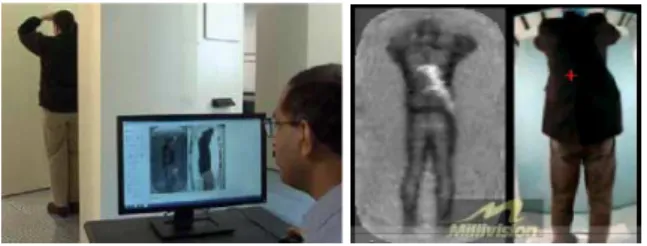
Fig. 1. Imaging applications. Detecting a concealed weapon
A chiral metamaterial cover is described and added over the antenna layer structure, both, in a single patch and in the 3 patch array, in order to improve the radiation properties. This novel cover has the potential to provide a higher gain and a narrower main lobe. The cover is composed of a circuit board with a pattern of rosettes printed on both metallization layers of the substrate, as will be seen later [3]. 3D electromagnetic results have been obtained using
several tools such as CST and Agilent EMPro 3D EM simulation software.
II. DESIGN OF THE ANTENNA ARRAY The final objective of this design is to obtain a good response in gain, with a value of about 13 dBi (typical gain in microstrip technology) and high directivity, initially centered around 96 GHz and with a -10 dB bandwidth about 7 GHz.
A. Theoretical Background
A preliminary design of a single aperture coupled patch antenna fed by slot was developed to evaluate the potential performance. The radiating microstrip patch element is etched on the top of the antenna substrate, and the microstrip feed line is etched on the bottom of the feed substrate. The thickness and dielectric constants of these two substrates may thus be chosen independently to optimize the distinct electrical functions of radiation and circuitry [4]-[5]. The details of the complete patch antenna are given in section B. In order to improve the radiation properties of the antenna, above all the gain and directivity, the patch antenna has been extended to a linear array composed of three patches. This type of antenna is characterized by using relatively cheap substrates and affordable manufacturing.
Moreover, a waveguide-to-microstrip transition has been included in the input of the antenna array to adapt the microstrip access to a waveguide input. The waveguide-to-microstrip transition is added for characterization purposes, but the antenna is conceived for a microstrip line environment. It is necessary to provide WR-10 waveguide connectivity (standard in W-band equipment) and compatibility with the auxiliary Millimeter Wave VNA extension modules of the network analyzer used for characterization [6]-[7].
B. Final Design
During the design, patch and slot dimensions were optimized taking into account input matching and gain. Their final dimensions were 1× 1.1 mm and 0.7 × 0.09 mm, for patch and slot, respectively.
Each patch is fed by a 100 Ω-microstrip line (dimensions: 3.7 × 0.09 mm). The three lines are connected to a 50 Ω-microstrip line of 0.26 mm length. This 50 Ω microstrip line is enclosed in a cut-off waveguide (dimensions: 1.14 × 0.55 mm), at a distance of 0.5 mm from the three-way junction (see more details in the manufacturing section), to propagate only the W-band Quasi-TEM microstrip mode. Other features of the design are: the phase center length between patches is 2.2 mm and the distance from the feed line to the case back is 0.5 mm.
The characteristics of the different design layers with their metallization are:
- The low-cost ULTRALAM 2000 substrate (εr = 2.5, tgδ = 0.0019, h = 4 mils and a copper thickness of 18 µm) is used in the deeper layer in order to avoid the propagation of higher modes with acceptable losses. This layer contains the 100 Ω feed line located on its rear face and the ground plane, where the slots are located, is on the upper face of the same layer.
- The intermediate layer is the radiant substrate, air, in this case, with a thickness of 5 mils. Two side supports composed of Rogers RT/Duroid 5880 substrate (h = 5 mils) are necessary to hold this air gap.
- The top layer is fabricated with Rogers RT/Duroid 5880 substrate (εr = 2.2 and tgδ = 0.0009 and h = 5 mils). It acts as a radome and holds the metallic patches on its bottom face. For a realistic simulation of the complete structure, the waveguide-to-microstrip transition was connected to the linear array of planar antennas excited by slots (see Fig. 2). Other details, such as metallic screws to join the different layers and the pieces of the metallic
structure, were also included in the final simulated design.
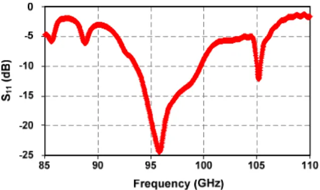
Fig. 2. Complete structure of the antenna array The input matching obtained from the 3D electromagnetic simulation is shown in Fig. 3. In this graph, we can see a -10 dB bandwidth of about 7 GHz with a minimum value at 96 GHz.
Fig. 3. Input Matching (S11) of the antenna array The most important parameter in the design of the antenna is its gain, so it is calculated in the simulations and it is plotted in Fig. 4.
G a in ( d B i)
Fig. 4. Gain of the antenna array
As can be seen, a gain value around 13 dBi is obtained, considered good, bearing in mind the number of patch elements of the array.
Fig. 5. Radiation pattern of the antenna array
Finally, we show the 3D pattern radiation in far field at 96 GHz (Fig. 5). A value of 13 dBi is reached in this frequency and a -14 dB Side Lobe Level is obtained [8], which is a typical value in this type of structure. Moreover, the achievement of a negligible backward radiation value should be highlighted.
C. Prototype Manufacturing
The fabrication of the prototype of our antenna has been done in two steps; on the one hand, the fabrication of all layers for the radiant elements which are defined with laser etching (very small dimensions with good accuracy) and on the other hand, the metal case, which is made in two pieces
with a tolerance of about 20-100 µm, depending on the accuracy needed in each part of the metal case. The dimensions of the complete structure are 4 × 3 cm.
The different layers that constitute the radiant elements are shown in Fig. 6, where the top and bottom faces of the lower layer and the upper layer can be seen. Furthermore, the two side supports needed between the two layers are also shown in the photograph.
Fig. 6. Photographs of the microstrip lines for the complete radiant system. (a) Feed lines and microstrip lines of the waveguide-to-microwave transitions, (b) ground and slots, (c) three array patches and (d) two side supports
Finally, all layers are placed within the metal case to complete the assembling of the prototype (see Fig. 7). A detail of the upper layer soldered on the metal case is displayed in Fig. 8.
Fig. 7. Total assembly of the complete antenna array It is interesting to note the complexity of the assembly due to several aspects: very small critical dimensions, tolerances in the fabrication process and misalignment errors with all layers used in the final structure.
Fig. 8. Zoom of the deeper layer within the complete radiant system
III. EXPERIMENTAL MEASUREMENTS
A. Measurement Setup
A N5242A PNA-X Microwave Network Analyzer was used for the experimental measurements. Two auxiliary Millimeter-Wave VNA extension modules were connected to the input and output ports of the setup to expand the analyzer to millimeter frequencies, specifically to W-band (both heads have WR-10 waveguide access).
All measurements shown were made under far field conditions. The input matching was the first measurement made, placing the prototype antenna at the port 1 head.
Then, the realized gain measurement was carried out in two steps. In the first place, two identical horn antennas, previously characterized, were placed in the setup, measuring their S21 parameter and calculating their gains (assumed equal) from this value. Then, one of these horn antennas was replaced by the antenna array under test, obtaining its gain by adding the differential value between the actual S21 and the previous S21 parameter to the horn antenna gain.
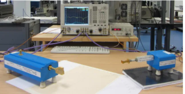
Regarding the radiation features, the radiation pattern in far field was obtained from two measurements. The azimuth plane measurement was carried out first, and the laboratory setup in this case can be seen in Fig. 9. Then, the antenna array was placed at port 1 and the horn antenna at port 2. The scanning was performed from -65˚ up to +65˚ in 5-degree steps, moving the horn antenna with respect to the array.
Fig. 9. Setup for the 2D radiation pattern in azimuth plane
To obtain the elevation plane in a simple and easy way (see Fig. 10), the horn antenna was placed at port 1, and the antenna array at port 2, turning its position vertically with respect to the measurement plane. The movement for obtaining the azimuth plane was done by the array, with the same sweep as for the azimuth plane measurements.
Fig. 10. Setup for the 2D radiation pattern in elevation plane
B. Measurement Results
In this section, all the results obtained from the experimental measurements are shown.
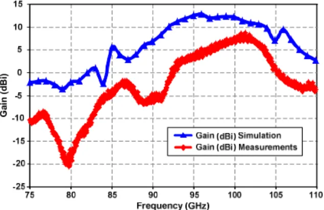
The measured input matching of the antenna array under far field conditions is compared in Fig. 11 to simulated results. From these results, we can see a good response with similar values although a frequency shift is observed (the minimum simulated S11 being at 96 GHz and the minimum measured S11 at 102.2 GHz), which is due to deviations between simulations and real implementations. It should be taken into account that in W band, the wavelength is very small (in the range of 3 mm in air) therefore any deviation in permittivity, thickness or positioning of a layer may produce a frequency shift. In a second iteration, this shift could be corrected readjusting the design. S1 1 (d B )
Fig. 11. Comparison of the input matching between simulations and measurements
The realized gain was the second measurement carried out in the laboratory (see Fig. 12). The shape of the measured gain compared with the simulated gain is quite similar in the range of frequency, and the maximum value of the measured gain is 8.7 dBi, lower than the simulated value of 12.7 dBi. This difference may be due to additional losses of the transition, access, setup used, etc.
G a in ( d B i)
Fig. 12. Gain: comparison between simulations and measurements
Finally, we present the 2D radiation patterns in the azimuth (Fig. 13a) and elevation (Fig. 13b) planes. It should be commented that the radiation patterns shown correspond to the minimum return loss frequency, which is 96 GHz for the simulations and 102.2 GHz for the measurements. Moreover, the radiation patterns are normalized to their maximum values.
It can be observed, in the comparison of both radiation patterns, from -65˚ up to +65˚, that there is an excellent result of the antenna array prototype with respect to the desired behavior. We can highlight the good value and shape of the side lobules regarding the main lobule in the azimuth plane, as well as a lack of directivity in the other plane as was expected.
-40 -40 -30 -30 -20 -20 -10 -10 0 dB 0 dB 90o 60o 30o 0o -30o -60o -90o -120o -150o 180o 150o 120o
Radiation Pattern with Theta=90deg
Simulation Measurements (a) -40 -40 -30 -30 -20 -20 -10 -10 0 dB 0 dB 90o 60o 30o 0o -30o -60o -90o -120o -150o 180o 150o 120o
Radiation Pattern with Phi=90deg
Simulation Measurements
(b)
Fig. 13. Radiation pattern of simulation and
measurement results (a) Azimuth plane, (b) Elevation plane
A comparison between measurement results and other references has been carried out. A W-band reference showing similar results in the same order of magnitude (8.56dBi of simulated gain for a single patch and 12.5dBi of gain simulated for three patch antenna in our case), using similar
substrate (εr = 2.2) is presented in [9]. The concept of stacked patch is used in [10], showing in a lower frequency range (55-70 GHz) similar gain (≥ 9 dBi) but higher bandwidth ( ̴ 14 GHz) than the proposed antenna. A 16 elements array of stacked patches in W band is presented in [11], showing higher gain (14.2 dBi) but at the cost of higher number of elements (more complex structure). Finally, gain, matching and particularly directivity results of the proposed antenna are in better agreement with simulations than the ones, also in W band, shown in [12], where a valuable analysis of discrepancies between simulated and measured results is presented.
IV. CHIRAL METAMATERIAL COVER TO ENHANCE THE RADIATION PROPERTIES
A. Chiral Metamaterial Cover
Good results have been obtained in the experimental measurements of the prototype antenna. As was seen in Section III.B, high directivity only exits in the elevation plane. Then, as a possible improvement in the directivity in the azimuth plane [13], a chiral metamaterial cover is presented in this section.
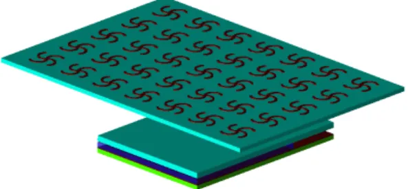
The chiral cover is a periodic structure with a unit cell consisting of two planar metallic rosettes printed on both sides of a substrate (see Fig. 14). The rosettes are parallel each other and one of them is twisted a certain angle with respect to the other one. This condition provides the property of 3D chirality to this structure. A detailed study of this structure is presented on [3].
To obtain the suitable dimensions of the unit cell we have followed 3 steps. First, rough dimensions of the chiral metamaterial structure were obtained scaling the structure presented in [3]. Next, the physical parameters were adapted to the constrains imposed by the substrate, mainly thickness of 5 mils and εr = 2.2. Finally, the geometric parameters were fine tuned to
adjust the electromagnetic response of the chiral metamaterial to the antenna response.
The rosettes structure is designed, using Agilent Empro simulator, to work in the same frequency band than the antenna. The dimensions of the unit cell are: radius = 166µm, width = 80µm and a copper thickness of 18µm. The relative twist of the rosettes is 15˚, and the dimensions of the unit cell dielectric substrate are 1 × 1 mm, with a thickness of 5 mils. The relative constant is 2.2 and tgδ = 0.0009.
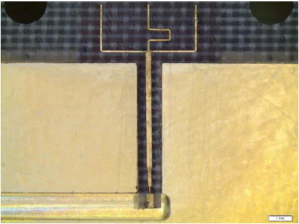
Fig. 14. Chiral metamaterial cover unit cell
B. Patch Antenna with Cover
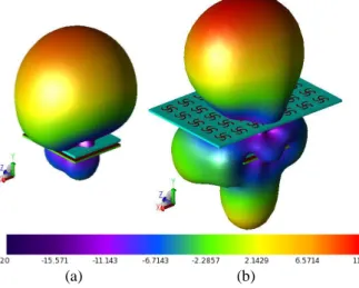
Before evaluating the influence of the cover on the linear array antenna, its effect on the radiation pattern of a single patch will be discussed. A chiral cover made up of a distribution of 7 × 5 pairs of aligned rosettes has been designed. It is placed over the antenna, parallel to the patch and separated from the radome as shown in Fig. 15.
Fig. 16 shows a comparison between the radiation pattern of the patch with and without the cover. The radiation pattern of the uncovered antenna, Fig. 16a, shows an 8.9 dBi gain and a large backward radiation, Front-to-Back Ratio (FBR) of 13.9 dB, due to the absence of a metallic plane in the bottom of the antenna system.
(a) (b)
Fig. 16. Radiation pattern of covered (a) and uncovered (b) single patches
When the cover is placed, Fig. 16b, it can be seen that the radiation pattern is focused along the normal direction to the patch. By comparing this radiation pattern to the single patch one, a gain increase is observed of around 2 dB and a main lobe width reduction of 20º is found for both azimuth and elevation planes: in the azimuth plane the 3 dB beamwidth decreases from 77º to 56º and in the elevation plane, it is reduced from 58º to 38º.
However, the structure exhibits an important backward radiation, with a very low FBR, 3 dB. It should be noted that an improvement in this parameter can be achieved by extending the ground plane.
Given the chiral nature of the cover, it is worth mentioning the polarization change that it produces on the radiated field. By introducing the chiral cover, the linear polarization radiated by
the patch is transformed into right-handed circular polarization.
C. Linear Array Antenna with Cover
In this section, the aforementioned cover is placed above the antenna array at a certain distance from it and between the two lateral screws, parallel and aligned to the radome (Fig. 17).
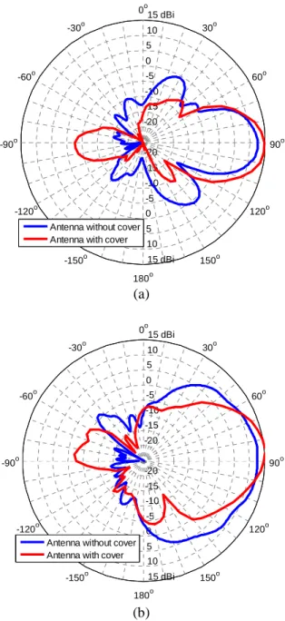
Fig. 17. Antenna with chiral metamaterial cover. In Fig. 18, a comparison is shown of radiation pattern (azimuth and elevation plane) simulation results with and without the cover. On inspecting this figure, it can be seen that the simulated gain is improved 2 dB (from 13 to 15 dBi) when the cover is included in the antenna structure. Moreover, the Side Lobe Level decreases 4 dB, from -16 dB up to -20 dB.
-20 -20 -15 -15 -10 -10 -5 -5 0 0 5 5 10 10 15 dBi 15 dBi 90o 60o 30o 0o -30o -60o -90o -120o -150o 180o 150o 120o Antenna without cover
Antenna with cover
(a) -20 -20 -15 -15 -10 -10 -5 -5 0 0 5 5 10 10 15 dBi 15 dBi 90o 60o 30o 0o -30o -60o -90o -120o -150o 180o 150o 120o Antenna without cover
Antenna with cover
(b)
Fig. 18. Radiation pattern with and without cover (a) azimuth plane, (b) elevation plane
Regarding the radiation pattern’s main lobe, the cover produces a narrowing in the response. So, on the one hand, in the elevation plane, the chiral metamaterial focuses the radiation pattern, as described in [14], in the broadside direction, reducing the 3 dB beamwidth 21˚, decreasing it from 57˚ to 36˚. On the other hand, in the elevation plane, the main lobe beamwidth has not
changed but the secondary lobes’ gain and beamwidth have been reduced.
Another aspect to remark in Fig. 18a, is that the main lobe in the elevation plane is deviated 5 degrees from broadside direction (θ = 90˚, φ = 90˚). This deviation is due to a slight misalignment between the three-patch array and the cover.
VI. CONCLUSION
In this paper, a design is presented of a high directivity antenna array in W-band. The final version of the antenna is composed of three patches fed by slots and featuring a waveguide-to-microstrip transition. This antenna has been fabricated and measured, and a comparison between simulation results and experimental measurements has been presented showing good agreement in input matching, gain and radiation pattern.
A chiral metamaterial cover added to the designed structure, both to the single patch and to the complete three-element array, has the potential to improve the antenna radiation features above all in the azimuth plane, where the antenna array does not have directivity. The cover has increased the gain by 2 dB, reduced the 3 dB beamwidth 21˚and the Side Lobe Level 4 dB.
ACKNOWLEDGMENT
The authors would like to thank to Sandra Pana for the fabricated samples of the available prototype and to Dermot Erskine for the correction of the text. This work has been partially supported by the MINECO of Spanish Government through the Research Projects CONSOLIDER 00068 and CSD2008-00066, FEDER co-funded TEC2011-29126-C03-01, TEC2011-29264-C03-01 and TEC2010-21496-C03-01.
REFERENCES
[1] S. Oka, H. Togo, N. Kukutsu and T. Nagatsuma, “Latest trends in millimeter-wave imaging technology”, Progress In Electromagnetics Research Letters, vol. 1, pp. 197-204, 2008 [2] R. Appleby and H. B. Wallace, “Standoff
detection of weapons and contraband in the 100 GHz to 1THz region”, IEEE Trans. Antennas Propag., vol. 55, no. 11, pp.2944-2956, Nov. 2007 [3] E. Plum, J. Zhou J. Dong, V. A. Fedotov, T.
Koschny, C. M. Soukoulis and N. I. Zheludev, “Metamaterial with negative index due to chirality”, Physical Review B, vol. 79, no. 3, pp. 035407-0355413, Jan. 2009
[4] D. M. Pozar,, “Microstrip Antenna Aperture-coupled To A Microstrip line”, Electronics Letters, Vol.21 No. 2,pp-49-50, 1985
[5] Amar, N.; Cabria, L.; Garcia, J.A.; Tazon, A.; Mediavilla, A.; Boussouis, M., "Equivalent Circuit of an Aperture Coupled Patch Antenna for Beam Control Applications," Electrotechnical Conference, 2006. MELECON 2006. IEEE Mediterranean , vol., no., pp.348,351, 16-19 May 2006. doi: 10.1109/MELCON.2006.1653110 [6] J. Gutiérrez, K. Zeljami, J.P. Pascual, T.
Fernández, A. Tazón, A. Mediavilla, E.S. Pana. “Yield-Oriented Design Protocol and Equivalent Circuit Model for W-Band E-Plane Waveguide-to-Microstrip Transitions”. International Journal of RF and Microwave Computer-Aided Engineering. DOI: 10.1002/mmce.20716. Volume 24, Issue 1, pp. 77-91. Jan. 2014
[7] J. Gutiérrez, O. Fernández, J.P. Pascual, A. Gómez, A. Tazón, A. Vegas, N. Amar. “Design and Fabrication of a W-Band Linear Array of Planar Antennas and Study for the Enhancement of its Radiation Properties with a Chiral Metamaterial Cover”. 4th International Conference on Multimedia Computing and Systems. 14-16 Abril 2014. Marrakesh. Morocco [8] N. Amar, L. Cabria, J. A. Garcia, A. Tazón, A.
Mediavilla and F. Marante, “A transmitting active array with spatially selective linealization”, The Second European Conference on Antennas and Propagation, EuCAP 2007 , pp.1-5, 11-16, Nov. 2007
[9] S. Agarwal, N.P. Pathak, D. Singh, "Performance comparison of microstrip patch antenna for 94 GHz imaging applications", 7th IEEE International Conference on Industrial and Information Systems (ICIIS) 2012, pp.1-4, 6-9 Aug. 2012. doi: 10.1109/ICIInfS.2012.6304781 [10] K. Li; T. Sato, N. Kajitani, "Wideband planar
antennas for millimeter-wave wireless communications", Antennas and Propagation Society International Symposium, 2008. AP-S
2008. IEEE, pp.1-4, 5-11 July 2008. doi: 10.1109/APS.2008.4619870
[11] A. Lamminen, J. Saily, "Wideband stacked patch antenna array on LTCC for W-band", Proceedings of the 5th European Conference on Antennas and Propagation (EUCAP), pp.2962-2966, 11-15 April 2011
[12] C. Meng, X. Zheng-hui, R. Wu, L. Wei-ming; W. Xiao-mo, "Research on W band microstrip patch antenna", International Conference on Microwave and Millimeter Wave Technology (ICMMT), 2012, vol.2, pp.1,4, 5-8 May 2012. doi: 10.1109/ICMMT.2012.6230082
[13] O. Fernández, A. Gómez, J. Gutiérrez, A. Tazón, A. Vegas, J.P. Pascual. "Enhancement of the radiation properties of a linear array of planar antennas with a chiral metamaterial cover", 9th Spanish Conference on Electron Devices (CDE), 2013, pp.223,226, 12-14 Feb. 2013. Valladolid, Spain. DOI: 10.1109/CDE.2013.6481383 [14] V.V. Gozhenko, J. Wigle, J. Vedral, B. Hendrix
and A.O. Pinchuk, “Focusing effect of a metamaterial slab on the radiation pattern produced by a patch antenna”, Metamaterials vol.6, Issues 1-2, pp. 37-42. Nov. 2012