Annealing Effect on the Structural and Optical Properties of SiOx films deposited by HFCVD
18
0
0
Texto completo
(2) https://cimav.repositorioinstitucional.mx/jspui. Introduction Non-stoichiometric silicon oxide (SiO x, x<2) films have been intensively studied because of their technological importance for silicon-based optoelectronic devices. SiOx can be considered as a multi-phase material composed of a mixture of stoichiometric silicon oxide (SiO2), not stoichiometric oxide (SiO x, x<2) and elemental silicon (as nanoparticles). Si nanoparticles (Si-nps) embedded in a SiOx matrix are currently attracting great interest as a candidate for efficient light absorber devices [1-3]. Such devices are highly desirable for the integration of optical signals with electronic data processing circuits in the same chip [4-5]. It has been established that blue and green photoluminescence (PL) observed in SiOx films are related by several emitting centers in the silicon oxide, while the nature of the intense PL in orange-red region is still discussed [6-8]. SiOx can be prepared by a number of techniques including silicon ion implantation into the thermal dioxide films [9], reactive sputtering [10-11], coevaporation [12], low pressure chemical vapor deposition (LPCVD) [13], Hot Filament CVD (HFCVD) [14] and plasma enhanced chemical vapor deposition (PECVD) [15]. In all of these techniques the silicon excess is controlled by changing the process parameters. Thermal treatments are generally used to enhance the luminescent properties of the SiOx films. In this paper, we report on the structural and optical properties (as Sinanocluster, amorphous silicon, defects, optical band gap energy and PL) of SiOx films deposited on silicon substrates with different Si excess. X-ray phothoelectron. 2.
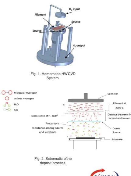
(3) https://cimav.repositorioinstitucional.mx/jspui. spectroscopy (XPS), Profilometry and Fourier transform Infrared spectroscopy (FTIR) techniques have been used to determine the structure and composition of SiOx films. The optical properties were obtained by PL and UV-Vis techniques. The optical band gap of the SiOx films; which are widened with respect to the bulk material (e-Si) and also, an intense visible room temperature PL to SiOx films is observed. Therefore, the influence of the Hydrogen flow in the Si excess is important, where the optical band gap increased depending of the parameters of deposit. Also, an interesting relationship between the growth temperature; annealing, gas flow, and structural and optical properties can be obtained and analyzed. With this knowledge it is possible to design SiOx films with a specific structural and optical characteristic just by a control of the gas flow and growth temperature, these features can be used to optoelectronics devices. Experiment SiOx films were deposited on n-type silicon wafers (100) with a resistivity of 1-1O Q-cm and on quartz substrates in a vertical homemade HFCVD reactor. The substrates were cleaned with a metal oxide semiconductor (MOS) standard cleaning process and the native silicon oxide was removed by a HF-Buffer solution. A schematic of the homemad e HFCVD configuration is shown in the Fig. 1. HFCVD technique consists in to dissociate molecular hydrogen in atomic hydrogen using a tungsten filament heated at 2000ºC. Atomic Hydrogen reacts with the source and it produces the precursors that are transported to the substrate.. 3.
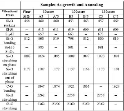
(4) https://cimav.repositorioinstitucional.mx/jspui. SiOx films were deposited at three different hydrogen flows 50, 100 and 150 sccm using quartz rods (of 5.3 cm length, 2 mm diameter) like source. The filamentsource distance and the distance source-substrate, which determines the growth temperature, were fixed at 3 mm and 5 mm, respectively. After deposition, SiOx samples were thermally annealed at 1100 C for 60 minutes in nitrogen atmosphere. Thermally annealed samples are marked as A3-T, B3-T and C3-T for hydrogen flow rates of 50, 100 and 150 sccm, respectively. Table 1 shows the characteristics of the growth films. Fig. 2 shows a scheme of the deposition process.. Fig. 1. Homemade HWCVD System.. Fig. 2. Scbematic ofthe deposit process.. 4.
(5) https://cimav.repositorioinstitucional.mx/jspui. The compositional and optical properties of the SiOx films were obtained using different spectroscopic techniques. FTIR measurements were done using a Brucker system model vector 22. XPS analysis was carried out using an ESCALAB 250Xi Thermo Scientific spectrometer with a monochromatic Al radiation XR15 and energy 20 eV. PL response was measured at room temperature using a Horiba Jobin Yvon spectrometer model FluroMax 3. The samples were excited with a wavelength of 240 nm, and PL response was recorded between 400 and 900nm with 1nm resolution. Transmittance of the SRO films was measured using a UV- vis-NIR Cary 5000 system from Agilent Technologies Inc. The transmittance was collected from 300 to 900 nm with a resolution of 0.5 nm. The thickness of SiOx film was measured by a profilometer DEKTAK 150 by Veeco Bruker with a Stylus of 12 µm.. 5.
(6) https://cimav.repositorioinstitucional.mx/jspui. Results. The thicknesses of the SiOx films are shown in Fig. 3. The FTIR absorption spectra of the SiOx films deposited with different Hydrogen flow before and after thermal annealing are shown in Fig. 4. Absorption peaks associated with the stretching (1084 cm-1) , bending (812 cm-1) and rocking (458 cm-1) vibration modes of the Si-O-Si bonds in SiO2 are observed in the SiOx films [15-16]. The position of the stretching absorption peak in SiO, films show different changes, this peak have a widened peak in the as-growth films, therefore different types of Si-O bonding conformed this stretching peak. The on phase stretching peak position moves toward a higher wavenumber with a larger growth temperature and the out of phase stretching peak position, similarly shows changes with the growth temperature. On the other hand, with annealing all peaks have a similar behaviour as SiO2 and a shited [sic] toward a higher wavenumber is observed.. 6.
(7) https://cimav.repositorioinstitucional.mx/jspui. 7.
(8) https://cimav.repositorioinstitucional.mx/jspui. Table 2 shows only the peak position of the Si-O, Si-Si, Si2O3, C-O, Si-C and SiH bonds to 50, 100 and 150 of gas flow. Fig. 5 shows XPS-Si 2p spectra and its evolution in the surface, volume (middle) and SiO x/Si interface (deep) of different SiOx films. The Si 2p binding energies are normally about 99-103 eV. lt is widely accepted that the Si 2p photoelectron peak of SiOx contains five components, corresponding to a non-oxidized state and four different oxidation states of Si [17-18]. The four oxidation states, as well as the unoxidized state, can be modeled as tetrahedral bonding units , in which a central Si atom is bonded to (4-n) Si atoms and n oxygen atoms (Si-Si4- 0O11) with n = O to 4. The variation of the oxidation states of the SiOx films lead to peak position's shift, as shown in Figure 5. Two main peaks at about 99 eV and 103 eV are 8.
(9) https://cimav.repositorioinstitucional.mx/jspui. present and they are attributed to Si and SiO2, respectively, and any variation could be attributed to sub oxidized silicon [19-20]. The increasing electro-negativity of the Si-O bound relative to the Si-Si bond results in a shift to a higher binding energy of the core level electrons in the silicon. Fig. 6 shows the XPS deep profile composition of different SiOx with different Hydrogen flow. The composition of SiOx is shown in Table III.. 9.
(10) https://cimav.repositorioinstitucional.mx/jspui. Figure 7 shows the PL spectra from SiOx films for the three different hydrogen flows. A wide PL spectrum is observed for all the as-growth samples. Two main peaks are placed around 690 and 750 nm and their intensity depends on the hydrogen flow. The PL peak placed at 700 nm is more intense as the hydrogen flow is increased. The PL quenches after the SiOx films are thermally annealed, at the same time that the presence of hydrogen disappears.. The Transmittance spectra display a wavelength shift of the absorption edge from 550 to 350nm to sample A3 and A3-T, respectively, as is show in the Fig. 8. The. 10.
(11) https://cimav.repositorioinstitucional.mx/jspui. transmittance of all films is among 70% to 80% from 500nm to 900nm and reduces to zero for wavelengths below 500 nm at 50sccm, 350nm at 100 and l 50sccm. lt implies a change in the optical band gap of the material, as it is shown in the Table IV. The optical band gap was obtained by Tauc plot method [20-21]; the results are illustrated in the table IV and Figure 9 shows an example.. 11.
(12) https://cimav.repositorioinstitucional.mx/jspui. Discussion The shape of the stretching peak in FTIR spectra let us differentiate between SiOx films as-growth and annealing. The stretching peak in SiOx films as-growth is. 12.
(13) https://cimav.repositorioinstitucional.mx/jspui. continuous and wide. However, with annealing the films show a thin stretching peak in FTIR spectra. The thin stretching peak means that the film is not amorphous and the shape of the peak looks like SiO2 stretching. In general, the stretching peak is defined by the hydrogen flow and the growth temperature. In case of 50 sccm, all the FTIR spectra of the SiOx films show that the stretching peaks have additional peaks with shape different to typical stretching Si. Diverse silicon-oxygen, silicon-hydrogen bonds and amorphous silicon form these SiOx films. In the FITR spectra of the SiOx films are observed typical stretching peaks (as SiO2) obtained at a hydrogen flow of 100 sccm as is show in the Fig. 4. The Si-Si bond appears near at 611 cm-1 Also, the increment of the intensity of H-Si bonds (663, 880 and 2250 cm-1) changed by the decrement of the temperature, it occurs during the deposition, which at the same time occurs an annealing and it forces the hydrogen (H) desorption. It was shown in previously works [14, 21]. The PL intensity of the SRO films is weak at higher temperatures. SiOx films growing to a hydrogen flow of 100 sccm and 5 mm of substrate-source distance showed the higher PL intensity. The decrement of the PL intensity at higher temperature is by desorption of H2, as it was shown by FTIR, where the highest deposition temperature the peak of Si-H at 870cm-1 is reduced with respect to the others temperatures deposition. Desorption of H2 increments the presence of nonradiative centers. The deposit at lO0sccm hydrogen flow with a substrate-source distance of 5 mm was showed a good homogeneity and highest intensity of PL. Our supposition about the. 13.
(14) https://cimav.repositorioinstitucional.mx/jspui. homogeneity is that the deposition temperature is constant over the substrate. On the other hand, the optical band gap is bigger to the sample deposit at 100sccm hydrogen flow and in all case the optical band gap increase with annealing.. Conclusion The properties of the films SiOx deposited by HFCVD presents different changes due to the growth temperature and the flows rate. The flows have high influence in the growth temperature. The deposit temperatures with a flow of 50sccm have a behavior different with respect other as growth films mainly in the stretching peak, as it was. 14.
(15) https://cimav.repositorioinstitucional.mx/jspui. observed by FTIR that shows the different types bond. In this case, the precursors remain more time on the substrate surface, but with annealing, a separation of phase is present. Desorption of Hydrogen was observed to highest temperatures with the annealing, and it has an effect strong in the PL. The PL tendency in each flow rate is that there is a temperature and flow with the better intensity PL. Therefore, the flow of hydrogen has influence strong in the PL. Films can be obtained by HFCVD with different characteristics structural and optical. The conditions to obtain SiOx films were developed in this study and these films showed very good absorption and emission of light. Acknowledgement This work has been partially supported by CONACyT- 154725 and VIEP-BUAP-2014. The authors acknowledge INAOE, IFUAP and CIMAV-Monterrey laboratory for their help in the samples measurements.. References. [1]. Nayfeh, M.; Rao, S.; Barry, N.; Therrien, J.; Belomoin, G.; Smith, A.; Chaieb, S.,. 2002, Appl. Phys. Lett., 79, 1249-1251. [2]. Pavesi, L.; Dal Negro, L.; Mazzoleni, C.; Franzo, G.; Priolo, F. 2000, Nature, 480,. 440-444. [3]. Luterova, K.; Pelant, I.; Mikulskas, I.; Tomaisiunas, R.; Mueller, D.; Grob, J.-J.;. Rehspringer, J.-L.; Honerlage, B. 2002, J. Appl. Phys., 91, 2896-2900.. 15.
(16) https://cimav.repositorioinstitucional.mx/jspui. [4]. Sui, G.G; Wu, X.L.; Gu, Y.; Boa, X.M. Appl. Phys. Lett. 1999, 74, 1812-1814.. [5]. Tamura, H.; Ruckschloss, M.; Wirschem, T.; Veprek, S. Appl. Phys. Lett. 1994,. 65, 1537-1539. [6]. Kenyon, A.J.; Trwoga, P.F.; Pitt, C.W.; Rehm, G. J. Appl. Phys. 1996, 79, 9291-. 9300. [7]. Lin, G. R.; Lin, C. J.; Lin , C, K.; Chou, L. J.; Chueh, Y.-L. J. Appl.. Phys. 2005, 97, 094306 [8]. Chen, X.Y.; Lu, Y.F.; Wu, Y.H.; Cho, B.J.; Liu, M.H. ; Dai, O.Y.; Song, W. D. J.. Appl. Phys. 2003, 93, 6311-6319. [9]. L. Pavesi, L. Dal Negro, L. Mazzoleni, G. Franzo, and F. Priolo, Nature, vol.408,. pp440, 2000. [10]. O. Hanaizumi, K. Ono , and Y. Ogawa, Appl. Phys. Lett , vol.82, pp.538- 540,. 2003. [11]. Kohno, K.; Osaka, Y.; Toyomura, F.; Katayama, H. Jpn. J. Appl. Phys. 1994, 33,. 6616-6622. [12]. Y. C. Fang, W. Q. Li, L. J. Qi, L. Y. Li, Y. Y. Zhao, Z. J. Zhang, and M. Lu,. Nanotechnology, vol.15, pp.495-500, 2004. [13]. D.Dong et al, J.Electrochem. Soc., vol.125, pp.819-823, 1978.. [14]. J. A. L. López, G. G. Salgado, A. P. Pedraza, O. E. V. Valerdi, J. C. López, A. M.. Sánchez, T. D. Becerril, E. R. Andrés, and H. J. Santiesteban, Structural and Optical. 16.
(17) https://cimav.repositorioinstitucional.mx/jspui. Properties of SiOx Films Deposited by HFCVD, Procedia Engineering, vol. 25, no. 2010, pp. 304-308, Jan. 2011. [15]. P. G. Pai, S. S. Chao, Y. Takagi, and G. Lucovsky, J. Vac. Sci. Technol. A, 4(3). (1986) 689-694. [16]. Pereyra, Alayo, Thin solid Films, 402 (2002) 154-161. [17]. Shinji Hayashi, Shinichi Tanimoto, and Keiichi Yamamoto: Analysis of surface. oxides of gas evaporated Si small particles with infrared spectroscopy, high resolution electron microscopy, and xray photoemission spectroscopy. J Appl Phys 1990, 68(1O): 5300. [18]. L.B. Ma, A. L. Ji, C. Liu, Y. Q. Wang, and Z. X. Cao: Low temperature growth of. amorphous Si nanoparticles in oxide matrix for efficient visible photoluminescence. J Yac Sci Technol B 2004, 22: 2654 [19]. F. lacona , G. Franzo, and C. Spinella: Correlation between luminescence and. structural properties of Si nanocrystals. J Appl Phys 2000 , 87(3): 1295. [20]. F. lacona, C. Borgiono, and C. Spinella: Formation and evolution of luminescent. Si nanoclusters produced by thermal annealing of SiOx films. J Appl Phys 2004, 95(7): 3723. [21]. J.A.Lun a López, J.C. López, D.E.Y. Valerdi, G.G. Salgado, T. Díaz Becerril, a. P. Pedraza , and F.J.F. Gracia, Nanoscale Res. Lett. 7, 604 (2012). [22]. Pankove JI: Optical Processes in Semiconductors. Englewood Cliffs, New. Jersey: Prentice Hall; 19 71.. 17.
(18) https://cimav.repositorioinstitucional.mx/jspui. 18.
(19)
Figure
Documento similar
In contrast to bulk Mn5Ge3 material which has uniaxial anisotropy along the c axis, epitaxial Mn5Ge3 films of thickness smaller than 50 nm exhibit an easy axis of magnetization lying
In Figure 6.15 we have plotted together the planar resistivity of all the c-oriented Lan+1 Nin O3n+1 films with different La/Ni composition deposited on NGO substrates, in a pure
In this thesis organic films have been grown by organic molecular beam de- position under different growth conditions and on different substrates to study the influence of
[22] who reported the influence of Nd doping on several properties of NZO films deposited on Si (1 0 0) by spray pyrolysis, showed that the samples exhibit ferromagnetic properties
