FACULTAD DE CIENCIAS
Chemistry Degree
Degree dissertation
SYNTHESIS AND CHARACTERIZATION OF PHOTOVOLTAIC
MATERIALS FOR LOW COST AND HIGH EFFICIENCY SOLAR
PANELS
SÍNTESE E CARACTERIZACIÓN DE MATERIAIS
FOTOVOLTAI-COS PARA PANEIS SOLARES DE BAIXO CUSTE E ALTA
EFI-CIENCIA
SÍNTESIS Y CARACTERIZACIÓN DE MATERIALES
FOTOVOL-TÁICOS PARA PANELES SOLARES DE BAJO COSTE Y ALTA
EFICIENCIA
Directors:
Manuel Sánchez Andujar
Socorro Castro García
“The consciousness of AC encompassed all of what had once been a Universe and brooded
over what was now Chaos. Step by step, it must be done.
And AC said, “LET THERE BE LIGHT!”
And there was light…”
INDEX
1 Abstract ... 7
1.1 English ... 7
1.2 Galego ... 8
1.3 Castellano ... 9
2 Introduction ... 11
2.1 Photovoltaic cells ... 11
2.1.1 Electronic band theory ... 11
2.1.2 Extrinsic semiconductors ... 14
2.1.3 The p-n junction ... 16
2.1.4 The silicon photovoltaic cell... 17
2.2 Dye sensitized solar cells ... 19
2.2.1 Origins of the DSSC ... 19
2.2.2 Solid-state DSSC ... 20
2.3 Perovskite crystal structure ... 23
3 Objectives ... 25
4 Experimental Procedure ... 26
4.1 Synthesis of the precursors ... 26
4.1.1 (CH3)2NH2I ... 26
4.1.2 CH3NH3I ... 27
4.1.3 Bulk synthesis of the perovskite ... 27
4.2 Preparation of the substrate ... 28
4.3 Deposition methods ... 28
4.3.1 One-step deposition ... 28
4.3.2 Two-step deposition ... 32
4.4 Additives ... 33
4.4.1 MACl as an additive ... 33
4.4.2 DMAX as additives ... 33
5 Instrumentation ... 35
5.1 X-ray powder diffraction (XRPD) ... 35
5.2 Scanning electron microscopy (SEM) ... 36
5.2.1 Fundaments ... 36
5.2.2 Instrument ... 37
5.3 Particle size measurement ... 38
5.4 UV-Visible ... 39
6 Results and discussion ... 41
6.1 Properties of the DMAPbI3 ... 41
6.1.1 Crystal structure and XRPD. ... 41
6.1.2 Optical properties ... 44
6.2 DMAPbI3 thin films ... 45
6.2.1 One-step technique ... 45
6.2.2 Two step technique ... 47
6.3 MACl as an additive in MAPbI3 precursor solutions ... 48
6.3.1 Particle size of the precursor solutions ... 49
6.3.2 Influences in thin film morphology ... 51
6.3.3 Presence of Chloride ... 52
6.4 DMAX and MAX as additives in DMAPbI3 precursor solutions ... 54
6.4.1 Change in particle size ... 54
6.4.2 Thin films ... 56
7 Conclusions ... 58
7.1 English ... 58
7.2 Galego ... 60
7.3 Castellano ... 62
8 Bibliography ... 64
1
ABSTRACT
1.1 English
This dissertation studies the use of the hybrid perovskite (CH3)2NH2PbI3 in solid-state dye
sensitized solar cells (ssDSSC), which was not previously described in the literature. To that end, thin films of the perovskite were prepared using both the one-step spin-coating and the two-step spin-coating techniques. Those films were characterized by XR powder diffraction and scanning electron microscopy. Furthermore, the UV-Vis spectrum of the compound was obtained, as well as its band gap and structure.
The UV-visible absorption spectrum of the (CH3)2NH2PbI3 revealed that it absorbed only in
the blue region and the ultraviolet zone, while its band gap was 2.81 eV. Although these optical properties are not adequate for photovoltaic applications, they it make an interesting candidate for use in a blue LED design. The structure of the compound is that of a hexago-nal perovskite, due to the big size of the dimethlyammonium cation.
At first, a non-homogenous layer of (CH3)2NH2PbI3 was deposited, with a needle-like
structure, and which was due to a large particle size of the precursor solutions. The particle size of the solutions was proved to be in relationship with the amount of organic com-pounds present in the solution, as it was reduced adding MAX or DMAX as additives (me-thyl or dimethlylammonium halides, where X is either Cl- or I-).
Also, this memory reports the influence of the additives in the particle size of the colloids and in film morphology on hybrid perovskite CH3NH3PbI3. The obtained results shown that
methylammonium chloride employed as additive induces a reduction of particle size of the precursor solutions leading to better, more homogeneous morphologies.
1.2 Galego
Este traballo estuda o uso da perovskita híbrida (CH3)2NH2PbI3 en células solares
sensitivi-zadas por colorantes de estado sólido (ssDSSC), a cal non fora descrito anteriormente na bibliografía. Para ese fin, capas finas da perovskita foron preparadas polos procedementos de spin-coating en un e dous pasos, respectivamente. Esas capas foron caracterizadas por difracción de raios-X en po e por microscopía electrónica de varrido. Ademais, o espectro de UV-Vis foi obtido, así como o seu bandgap e a súa estrutura.
O espectro de absorción de UV-visible do (CH3)2NH2PbI3 revelou que este solo absorbía na
rexión ultravioleta, mentres que o seu band gap era 2.81 eV. Aínda que estas propiedades non eran adecuadas para aplicacións fotovoltaicas, tamén o fan un candidato interesante para o seu uso nun LED azul. A estrutura cristalina do composta é a dunha perovskita he-xagonal, debido o gran tamaño do catión dimetilamonio.
Ao principio depositouse unha capa non homoxénea de (CH3)2NH2PbI3, cunha estrutura en
forma de agullas, o calé debido ao gran tamaño de partícula das disolucións precursoras. Demostrouse que o tamaño de partícula das solución precursoras esta relacionado coa can-tidade de compostos orgánicos presentes na disolución, xa que foi reducido ao engadir MAX ou DMAX como aditivos (haluros de metil o dimetil amonio, sendo X ben Cl- ou I-). Esta memoria tamén reporta a influencia dos aditivos nos coloides e na morfoloxía das ca-pas da perovskita híbrida CH3NH3PbI3. Os resultados obtidos mostran que o emprego de
cloruro de metilamonio como aditivo induce unha redución do tamaño de partícula das solución precursoras, levando á obtención de morfoloxías mellores e máis homoxéneas.
1.3 Castellano
Este trabajo estudia el uso de la perovskita hibrida (CH3)2NH2PbI3 en células solares
sensi-tivizadas por colorantes de estado sólido (ssDSSC), el cual no había sido descrito anterior-mente en la literatura. Para tal fin, capas finas de la perovskita se prepararon usando las técnicas de spin-coating en uno y dos pasos. Esas capas fueron caracterizadas por difrac-ción de polvo de rayos-X y por microscopía electrónica de barrido. Además, se obtuvo el espectro UV-Vis del compuesto, así como su band gap y su estructura.
El espectro de absorción de UV-Vis del (CH3)2NH2PbI3 reveló que solo absorbe en la zona
azul y la ultravioleta, mientras que su band gap es de 2.81 eV. Aunque estas propiedades no son adecuadas para aplicaciones fotovoltaicas, hacen del compuesto un candidato interesan-te para su uso en un LED azul. La estructura cristalina del compuesto es la de una perovski-ta hexagonal, debido al gran perovski-tamaño del ion central.
Al principio se depositó una capa no homogénea de (CH3)2NH2PbI3, con una estructura en
forma de agujas, y que es debida al gran tamaño de partícula de la disoluciones precursoras. El tamaño de partícula de las disoluciones, a su vez, se demostró que está relacionado con la cantidad de compuestos orgánicos presentes en la muestra, ya que se redujo al añadir MAX o DMAX como aditivos (haluros de metil o dimetil amonio, siendo X bien Cl- o I-). Asimismo, esta memoria reporta la influencia de los aditivos en el tamaño de partícula de los colides, así como en la morfología de las capas de perovskita híbrida CH3NH3PbI3. Los
resultados obtenidos muestran que el uso de cloruro de metilamonio como aditivos induce una reducción del tamaño de partícula de las disoluciones precursoras, llevando a la obten-ción de morfologías mejores y más homogéneas.
2
INTRODUCTION
At this point, it has become almost a cliché to state the need for clean and renewable sources of energy. Nevertheless, the search to cover this need is probably one of the great-est challenges facing humanity in this century. The overreliance in non-renewable and pol-luting sources of energy, such as coal, natural gas and the infamous oil, has created a sys-tem that is not sustainable. Furthermore, the emission of greenhouse gases (CO2 being the
most famous) has provoked an anthropogenic climate chaos that jeopardizes not only the survival of countless species, but the means of living of many societies. All these are un-disputable facts, with almost unanimous scientific consensus behind them1, that need to be addressed. And while it is true that a successful response to climate change cannot only be technological in scope, science and technology still play a crucial part in overcoming this challenge. Ever since they saw widespread use, the solar cells have been put as an example of the clean and renewable energies needed for the future. However, many aspects still need to be improved: the current photovoltaic cells require high purity silicon, doped with sever-al scarce elements, such as Gsever-allium and Indium which greatly increase the price of the cells, as well as their availability. New research should focus in overcoming these issues, as well as improving performance, and the new solid-state dye sensitized solar cells show promising characteristics.
2.1 Photovoltaic cells2
Solar cell can be divided in those based in the technology of silicon semiconductors and those based in the dye sensitized solar cell technology. While this dissertation will focus on the second ones, it is still necessary to understand the silicon based solar cells, since they are the basis upon the technology is based. Furthermore they remain the benchmark against which all new cells are measured.
2.1.1 Electronic band theory3
To comprehend the photovoltaic effect, which is the basis for any solar cell, an understand-ing of the principles of semiconductors is vital. These materials, which form the basis of
much of modern technology, can be though as a middle ground between conductors, able to conduct electrical current with little resistance, and insulators, unable to do so. These prop-erties can be explained through the electronic band theory.
The electronic band theory states that in any solid with a large number of atoms, N, the in-dividual electronic states of the atoms begin to split into closely separated states, due to the interaction with other atoms. While at first an energy gap may exist between the individual electronic states, soon it becomes small enough to be able to talk about a continuous elec-tron energy band. However, some energy levels may remain empty of elecelec-tron energy bands, since no electronic state has those energies. These forbidden spaces usually form gaps between the different bands.
The number of states present in every band equals the number of states contributed by the N
atoms of the solid; so an s band will have N states and a p band, 3N. The number of elec-trons will also be equal to the number of elecelec-trons originally present in the isolated atoms. As a consequence, bands may be partially filled, or even empty of electrons. The energy of the highest filled state at 0 K is called the Fermi level, Ef. Different electron band structures
are thus possible, as shown in Figure 2.1, and are as follows:
Figure 2.1
Electronic band structures of conductors, insulators and semiconductors
- Conductors: This is characteristic for metals, for which the number of possible states is greater than the number of valence electrons. As a result, the valence band is only partially filled, and the Fermi level is located within it.
- Insulator: For these materials the so-called valence band is completely filled; and the only empty states are located in the conduction band, which is completely emp-ty. Both bands are separated by a large energy band gap, where the Fermi level is located. This band gap is usually greater than 2 eV.
- Semiconductors: Their structure is almost identically to an insulator, with a com-pletely filled valence band and a comcom-pletely empty conduction band. The energy band gap between them, however, is much smaller than in an insulator, less than 2 eV, and can be overcome by some electrons under the right circumstances.
Conduction of electrical current requires electrons to have energies larger than the Fermi level, becoming free electrons. In the case of conducting materials this is easily achieved. As shown before, the Fermi level is within the band itself, so the energy required to pro-mote electrons above it is rather small. Usually, the energy coming from the electric field itself is more than enough. For insulators and semiconductors, however, the band gap lies between the highest filled state and the lowest empty state still above the Fermi level. To be able to conduct, an external source, such as light or temperature, must give the electrons enough energy to overcome the band-gap. In the case of insulators, the band gap is too large to be overcome by those sources, so they are not able to conduct under most circum-stances. For semiconductors, however, the band gap is small enough to be overcome, pro-moting electrons from the valence band into the conduction band, where they become free electrons. Despite this, the conductivity of semiconductors will remain lower than that of the conductors, and be highly dependent on the temperature.
When an electron is promoted into the conduction band, an empty electronic state is left in the valence band. This empty state can be re-filled by other electrons, leaving another emp-ty state in turn. Thus, it is convenient to treat a vacant state as a positively charged particle called a “hole”. This particle would have the same charge that the electron, only positive, and can also take part in the conduction of electrical current in semiconductors. If a hole
and a free electron meet, they will recombine, filling the empty vacant state. Both free elec-trons and holes are known collectively as charge carriers.
2.1.2 Extrinsic semiconductors
The semiconductors described above are intrinsic semiconductors, that is, their electronic properties depend only on their electronic band structure. However, most of the semicon-ductors employed nowadays are extrinsic semiconsemicon-ductors, where the electronic properties also depend on small impurities of other elements introduced to the material. This impuri-ties need to be introduced with great care, in a process known as doping, since concentra-tions of just one atom in every 1012 Si atoms can turn silicon into a extrinsic semiconductor. Depending on the nature of the doping elements, the extrinsic semiconductors are classified in p-type and n-type semiconductors. Both are schematized in Figure 2.2, and are as fol-lows:
- n-type semiconductor: In this case, the silicon is doped with small amounts of an el-ement with more valence electrons (such as P, As or Sb). Those extra electrons are located in the so-called donor states, situated just below the conduction band of the silicon. At room temperature, thermal energy is enough to promote some electrons from the donor states to the conduction band, where they become conducting free electrons. Since all free electrons come from the donor states (the intrinsic effects are usually negligible) no corresponding hole is formed in the valence band, thus all conductivity in n-type semiconductors is due to free electrons, and is a function of both temperature and donor concentration.
- p-type semiconductor: They are the opposite of the n-type semiconductors. They are doped with elements with less valence electrons than silicon (such as B, Al or Ga). Those elements introduce empty electron states just above the valence band, with low enough energy to accept electrons coming from the valence band, called accep-tor states. The promoted electrons leave behind in the valence band positively charged holes that can conduct charge in an analogous way to the free electrons in the conduction band. Similarly, no free electrons are promoted to the conduction band, and conductivity is only due to the holes in the valence band.
Figure 2.2
The two types of extrinsic semiconductors
2.1.3 The p-n junction
The p-n junction, one way or an-other, is the basis of many current electronic devices. One of the most basic ones, but which exemplifies very well the principles behind the p-n
junction is the diode, or a rectifier. It is a device that only allows the current to flow in a direction, and it is made from one piece of a semiconductor, doped in ones side to be a p-type and
n- type in the other. This way, any external electrical potential can be established in two different ways: When the positive terminal of a bat-tery is connected to the p-side and the negative terminal to the n-side, then it is referred as a forward bias. The op-posite polarity is known as reverse bias. The three possibilities (no bias, forward bias and reverse bias) are rep-resented in Figure 2.3.
- When no bias is present, both sides act as normal extrinsic semiconductors. In the p-side the majority of charge carriers are holes, while in the n-side they are electrons.
- When a forward bias is applied new electrons ae injected into the n-side, which flow to the junction. Similarly, holes in the p-side are also attracted to the junction. There; in the so called recombination, or depletion, zone; holes and electrons
con-Figure 2.3
The three different bias of a diode
tinually recombine and annihilate each other. Since there is a continuous flow of charge carriers, the electrical current can be conducted.
- When the reverse bias is applied both holes and repelled from the junction and no recombination takes place. The flow of charge carriers is interrupted and the diode becomes an insulator.
2.1.4 The silicon photovoltaic cell4
The principles explained above for the p-n junction also apply to the silicon photovoltaic cell. The basis of a photovoltaic cell is a p-n junction, in which the p-side is much thicker than the n-side. Because of that, most of the photons coming from sunlight are absorbed either in the recombination zone or in the p-side.
If the photon has an energy greater than the band-gap of the semiconductor (1.1 eV for Sili-con), it is able to promote one electron from the valence band into the conduction band. Thus, an electron-hole pair (EHP) is generated. If the EHP was generated within a certain diffusion length, Le for electrons and Lh for holes, then the electrons are able to diffuse
Figure 2.4
Electronic band diagram of a solar cell
back into the recombination zone. If the EHP is created outside those distances, then re-combination will take place before any diffusion. The charge carriers that reach the junction are swept back into the n-side if they are electrons and into the p-side if they are holes. If an electrode is attached to each side, then an electrical current is generated. The whole process is summarized in Figure 2.4. There, the electronic bands of the solar cell are shown, as well as the energy path of the generated electron.
For obvious reasons, the band gap of the semiconductor is crucial to the performance of the solar cell. Small bandgaps are often more desirable, since less energy is required to promote electrons to the conduction band. However, the extra energy of photons above the band gap is usually lost in form of thermal, rather than electric, energy, lowering the efficiencies. It should be noted that, since most of the sunlight belongs either to the visible light or the near infrared, solar cells need to be optimized to work at those frequencies.
One way of trying to surpass the inherent limitations of conventional solar cell was the de-velopment of multijuction photocells, also known as tandem solar cells. These cells consist of several layers of semiconductors stacked in top of each other, each one with a different band gap. The top layer semiconductors, with higher band gaps, absorb higher energy tons; while the bottom semiconductors, with lower bad gaps, absorb the lower energy pho-tons. This has allowed solar cell to achieve efficiencies never seen before. Another devel-opment of the silicon solar cell was the thin-film solar cell using amorphous silicon. The numerous grain boundaries lead to a higher band gap that more efficiently captures sun-light.
However, all silicon based solar cells face the same economic problems. They rely on a supply of high purity silicon, and while silicon is an abundant element, the necessary puri-fication is an energy intensive process. Furthermore, the growing demand of silicon for use in solar cells conflicts with the also growing demand of silicon for use in electronic appli-ances. While there is undergoing research to produce solar-quality silicon in a cheaper way, they have yet to be successful5. Furthermore, almost all types of solar cells require quanti-ties of Gallium and Indium, elements with a low concentration on the Earth’s crust. Those
could become a dangerous bottleneck that could limit the expansion of the photovoltaic technology6.
2.2 Dye sensitized solar cells7
To overcome the problems faced by the conventional, silicon based solar cells, a radically new approach began to take form in 1960’s. Moving away from silicon based alternatives, a new type of solar cell was developed in which light absorption and charge generation took place in different devices. Since the light absorption originally took place in an organic dye, this type of cells came to be known as dye sensitized solar cells, DSSC.
2.2.1 Origins of the DSSC
While the first paper studying the possibilities of photoelectrochemical cell dates back to 18878, and by 1965 the first working cells had already been constructed9; it was only in 1991 when the first major breakthrough was achieved. Using a mesoporous TiO2 film,
O’Reagan and Grätzel were able to dramatically increase the surface area of the dye, lead-ing to higher efficiency in the conversion of photons10. This mesoporous TiO2 layer would
become an integral part of all future designs, including solid-state DSSC (ssDSSC), until it was replaced by a compact layer of TiO2 in the later perovskite based solar cells.
The basics of a DSSC cell are not dissimilar to those of the silicon solar cell: An electron-hole pair is formed by the absorbed energy of the photons; then, the charge carriers flow back to their respective electrodes, creating an electric current. Keeping these basics in mind is easy to understand the working of a DSSC, as shown in Figure 2.57, which consists of the following processes:
1. Excitation of the dye to a higher energy state by a photon.
2. Electron injection by the dye into the metal oxide (usually TiO2).
3. Electron transport to the working electrode. 4. Excited-state decay of the dye.
5. Regeneration of the excited dye by electron transfer of the donor species. 6. Hole transport to the counterelectrode.
7. Transport of electrons from the working electrode to the counterelectrode, generat-ing electrical current.
8. Regeneration of the oxidized donor.
The donor species is usually an I3- /3I- redox system in a liquid ionic electrolyte.
2.2.2 Solid-state DSSC
It was soon proved that the use of liquid electrolytes led to serious problems of corrosion, as well as hindering the true potential of the DSSC. This is due to the overpotential required to oxidize the electrolyte11. To mitigate those issues, it was attempted to exchange the liq-uid electrolyte and the I3- shuttle with some kind of solid hole-transporting material, or
HTM. The first cell to achieve this was reported in 1998, and it used an amorphous organic
Figure 2.5
Schematized energy diagram of a DSSC7
material; 2,2’,7,7’-tetrakis(N,N-di-p-methoxyphenyl-amine)9,9’-spirobiflourene (spiro-OMeTAD); as the HTM12. Soon, all DSSC that did not use a liquid electrolyte were known as solid-state DSSC, or ssDSSC, and became the new front of research.
The new ssDSSC were not without their drawbacks, however. One crucial step to be re-solved was to achieve a good pore filling of the TiO2 layer by the dye13. Failure to this
caused a limitation on the thickness of the cells at a level below the optical depth of the composite, causing a performance below the theoretical maximum. Several methods were tried to improve pore filling, and it remains one of the main challenges in the development of the ssDSSC.
Simultaneously, improvements to the organic dyes used in the original DSSC were also researched. Eventually, the possibility of employing p-type semiconductors as sensitizers was studied14. Inorganic sensitizers had high molar extinction coefficients, which led to better light absorption. Several materials were tried until the research led to the use of hy-brid inorganic-organic perovskites, such as methylammonium lead iodide, CH3NH3PbI3
(MAPbI3), as sensitizer. MAPbI3 first used in a traditional liquid DSSC, but this cell failed
due to the dissolution of the perovskite in the electrolyte15. Soon, they were also employed in ssDSSC, but these devices keep employing spiro-OMeTAD as the HTM16. However, it was discovered that the perovskite could also act as the HTM itself. Nevertheless, a HTM is still in use by most current devices.
The structure of a perovskite ssDSSC is shown in Figure 2.617. Above a substrate of conducting glass, a compact layer of TiO2 is
deposited. Above it lays the perovskite layer, acting as the light absorber. The perovskite, in turn is covered by the HTM, typically the spiro-OMeTAD. A metallic layer at the top
Figure 2.6
Schematized energy diagram of a DSSC17
finally acts as the counterelectoder, closing the circuit. A smooth and homogeneous cover-ing is required, free of pinholes, since if unwanted contacts were to exist between the non-consecutive layers (such as a contact between the TiO2 and the HTM, or the perovskite and
the countereectrode), no photovoltaic effect will occur. There is, however, still some debate regarding the best deposition technique to achieve it. The most commonly used perovskite is the CH3NH3PbI3, but similar compounds with either bromide or chloride had been tried
as well18. Perovskites with formamidinium as the organic part or Cs as the metallic cation were also tried, but they were proven to have less efficiencies that the MAPbI3 compound.
The research regarding perovskite ssDSSC has seen a dramatic increase, tied with the in-crease in performance of the cells. Both effects are shown in Figure 2.7, which shows the number of publications about perovskite solar cells as of 2/1/201519. The perovskite solar cells are an exciting topic in today’s material science research and will continue to be so in
Figure 2.7
Growth of both research and efficiency of perovskite solar cells19
the foreseeable future.
2.3 Perovskite crystal structure20
It is doubtful that when Gustav Rose discovered the calcium titanate (CaTiO3) in Russia
and decided to name it after the Russian mineralogist L. A. Perovski he could imagine the importance of his discovery for the future of solar cells18. Regardless of that, it was soon realized that many other compound shared the same peculiar crystal structure of the new mineral, so they began to be called by the same name. This way, compounds with perov-skite structure have a generic formula of ABX3, where A and B are cations of very different
sizes, the A cation being larger, and X is an anion.
The ideal perovskite structure of a compound ABX3 has a cubic unit cell, where each A
cation is surrounded by 12 X anions inside a cubooctahedral, and each B cation is sur-rounded by 6 X anions forming BX6 octahedra. Meanwhile, the BX6 octahedra themselves
form a three dimensional structure in which every octahedron shares all of its vertexes with neighboring octahedra. In the cavity created by eight of those octahedra is located the A cations, balancing the whole structure. This structure can be seen in Figure
2.8.
The ideal cubic perovskite structure is only reached when the ionic radii of A,B and X ions fulfill a particular crite-rion. If the ionic radii are out of the ideal ratio, the compound displays a distorted perovskite crystal structure with a cooperative tilting and rotation of the BX6 octahedra. Its crystal
sym-metry also becomes lower than the ideal cubic cell. To predict this effect,
Figure 2.8
Structure of a perovskite
a tolerance factor, t, was proposed by Goldschmidt in the early 1920. It follows the follow-ing formula21:
𝑡𝑡
=
𝑟𝑟
𝐴𝐴+
𝑟𝑟
𝑋𝑋√
2(
𝑟𝑟
𝐵𝐵+
𝑟𝑟
𝑋𝑋)
Where rA, rBand rX are the ionic radii of the cations A and B, and the anion X. For an ideal cubic structure t should be equal to 1. However, since the Goldschmidt factor deals with ionic radii, it should be remembered that it is just a semi-empirical formula. In reality, structures with t within 0.9 and 1.0 remain their cubic structure. This range is broadened when the distorted structures are also taken into account22.
The most commonly used perovskite for photovoltaic applications, the MAPbI3, is a
some-what peculiar example in that the Pb2+ cation takes the B position, while it commonly oc-cupies the A position. This unusual location is only possible because a large electropositive cation, (CH3NH3)+, occupies the A position23.
3
OBJECTIVES
The main objective of this dissertation is the synthesis and characterization of hybrid organ-ic-inorganic perovskites for its possible use in solid-state dye sensitized solar cells. The focus will be on the hybrid perovskites (CH3)2NH2PbI3 and CH3NH3PbI3, and their
capabil-ities as light absorbers. Furthermore, the particle size of the colloids of the precursor solu-tions will be studied, as well as its relasolu-tionship with the thin film morphologies and the in-fluence of various additives.
To that end, the following steps will be taken:
- Synthesis of the precursor compounds: (CH3)2NH2I (DMAI) and CH3NH3I (MAI)
- Measurement of the particle size of the colloids in the precursor solutions.
- Deposition of thin films in glass substrates using the one-step spin-coating and the two-step spin-coating techniques.
- Study of the optical properties of the DMAPbI3 compound.
- Characterization of all the obtained thin films using XR powder diffraction and the Scanning Electron Microscopy (SEM).
- Study of the effect of the MACl as an additive on the MAPbI3 precursor solutions,
both in particle size and thin film morphology.
- Study of the effect of various additives on the DMAPbI3 precursor solutions both in
particle size and thin film morphology.
4
EXPERIMENTAL PROCEDURE
4.1 Synthesis of the precursors
Before any work could be done on the deposition of the thin films themselves, the precur-sors had to be synthetized, since neither the methyamonnium iodide (CH3NH3I) nor the
dimethylammonium iodide ((CH3)2NH2I) were commercially available. The method
em-ployed for the synthesis was described in the bibliography24, if somewhat sparingly.
4.1.1 (CH3)2NH2I
12 mL of dimethylamide 40% (wg.) in water (0.0949 mol) were dissolved in 50 mL of eth-anol in a round-bottom flask. 5 mL of hydriodic acid 47% (wg.) in water (0.0275 mol) were added while under magnetic stirring in an ice and water bath. After letting the mixture react for an hour the solvent was eliminated in the rotary evaporator. An orange precipitate was formed on the walls of the flask. That precipitate was redissolved in 10 mL of heated etha-nol and transferred to a crystallizer. The mixture was left for a day to recrystallize, even though some white crystals had already began to form when the ethanol cooled. The next day, the product dimethylammonium iodide (DMAI) was recovered by vacuum filtration and washed with small quantities of cold ethanol.
It should be noted that, even though the bibliography indicates the washing with diethyl ether, when that was attempted the DMAI was immediately dissolved and washed to the Erlenmeyer flask. The ether had to be eliminated in the rotary evaporator and the product recrystallized once again. It was recovered by vacuum filtration and washed with cold etha-nol, as already mentioned.
The DMAI was in the form of a white powder, which was sent to XRPD for analysis. A total of 1.644g of product was obtained, achieving a yield of 34.5%. This quantity was enough for all the made thin films, and there was no need to repeat the synthesis.
4.1.2 CH3NH3I
A similar method to the one used in the synthesis of DMAI was used for the methylammo-nium iodide (MAI), only with bigger quantities of both reagents and solvent. 24 mL of me-thylamide 33% (wg.) in ethanol were mixed with 10 mL of hydriodic acid (same as before) in 100 mL. The reaction time was also longer, at 2 hours, after which the solvent was elim-inated in the rotary evaporator. This time the product recovered by the vacuum evaporation was washed directly with cold ethanol.
The product was also in the form of a white powder, which was sent to XR powder diffrac-tion (XRPD) for analysis. Since the MAI was more commonly used than the DMAI, the synthesis of the former had to be repeated several times.
4.1.3 Synthesis of the bulk perovskite
The synthesis of the perovskite was attempted using a mortar. To that end 75 mg of DMAI (4.33 ∙ 10-4
mol) were mixed with 200 mg of commercially available PbI2(4.33 ∙ 10-4 mol)
in a mortar to obtain DMAPbI3, which still had a white color.
The MAPbI3 was also synthesized in a mortar, mixing stoichiometric quantities of MAI and
PbI2. In this case there was a dramatic change of color: from the yellow of the PbI2 and the
4.2 Preparation of the substrate
The substrates employed at the beginning were originally glass specimen holders for an optical microscope, manually cut to the required size (approx. 3x3 cm). To avoid the inter-ference of dust in the deposition of the films the substrates were thoroughly washed with distilled water with soap and then rinsed with more distilled water.
Halfway during the experimental procedure new glass substrates with a layer of a conduc-tive material were obtained. These could better simulate the morphology of a proper solar cell and were used from that point onwards. The thin films were only deposited on the con-ductive layer.
4.3 Deposition methods
Two methods were employed for the deposition of the thin films: the one-step deposition and the two-step deposition. These were found in the bibliography25 and were reproduced in the laboratory.
4.3.1 One-step deposition
In the one-step spin-coating technique, a precursor solution of the desired product is pre-pared. This solution is spread over the substrate with the help of a spin-coater. The sub-strate is then heated, so all the solvent evaporates, leaving just a thin film of the perovskite.
In the one-step procedure, a precursor solution of both PbI2 and MAI (or DMAI) is
pre-pared beforehand. To that end 0.395 g of MAI and 1,157 g of PbI2 are dissolved in 2 mL of
dimethylformamide (DMF), to obtain a solution with a 1.25 M concentration of MAPbI3.
When preparing the precursor solution of DMAI, instead of MAI, 0.363 g of DMAI was dissolved with the same amount of PbI2. Since the PbI2 proved difficult to dissolve, the
solutions are left heating (at around 60° C) under magnetic stirring overnight. Finally, a yellow solution of MAPbI3 is obtained. The DMAPbI3 has a more orange color.
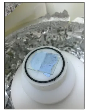
The substrate is attached to the moving part of the spin-coater with the help of some blue-tack, as shown on Figure 4.3. Then, the precursor solution is placed on top of the substrate with a micropipette, and spread until it covers all the substrate, like in Figure
4.4. Initially the volumes of the precursor solution were as low as 20 µL were used, but it was soon proved that they were unable to completely cover the substrates. The amounts were progressively increased to 150 µL. Once the substrate is covered with the solution, the spin-coater is started, with the following parameters:
- Acceleration: 500 rpm/s
- Maximum speed: 3000 rpm
- Total run time: 20 s
Figure 4.3
Attaching the substrate
Figure 4.4
Spreading the precursor solution
Figure 4.5
Substrate on the hot plate
Figure 4.6
Substrate after the spin-coating
Those parameters were left unchanged in all experiments, unless otherwise noted. After the spin-coater had stopped, it would seem like there was no solution left in the substrate, as shown on Figure 4.5. However, once the substrate was placed on a hot plate a black color will soon star to show, as in Figure 4.6. The substrate was left on the hot plate for about 5 minutes, at a temperature of approximately 70° C. Afterwards it was transferred to an oven at 100-150° C and was left heating for another five minutes. After recovering the substrate the black color had intensified, as can be seen in Figure 4.7.
The one-step deposition technique was the most used technique throughout the whole pro-cedure, and the obtained films were used to measure the optical properties.
Figure 4.7
Substrate after the heating treatment
4.3.2 Two-step deposition
The two-step deposition technique is a variation of the one-step technique. In this version the two reagents needed for the synthesis of the perovskite, PbI2 and DMAI, are deposited
separately on the substrate. First, the substrate is covered by spin-coating a solution of PbI2
and then the solvent is evaporated in the oven. The resulting film thin is submerged in a solution of DMAI and the solvent evaporated again in the oven. The technique is resumed in the Figure 4.8.
The precursor solution of PbI2 was prepared dissolving 0.9231 g of PbI2 in 2 mL of DMF,
to achieve a concentration of 1 M. The PbI2, however, proved extremely difficult to
dis-solve in DMF, needing long times of heating and magnetic stirring. Furthermore, after the heat and the stirring were removed, the PbI2 tended to precipitate again. Despite these
diffi-culties, a solution stable enough to be spin-coated was obtained. The parameters used in the first deposition were identical to those of the one-step technique (Acceleration: 500 rpm/s; speed: 3000 rpm; time: 20 s). The solvent was evaporated in the hot plate for 4 minutes and then in the oven for another five minutes, at 100° C. A yellow thin film of PbI2 was
ob-served to be formed.
A second solution was prepared, dissolving 40 mg of DMAI in 2-propanol, to achieve a concentration of 0.063 M. The substrate previously covered with the thin film of PbI2 was
submerged in this new solution for a minute. Then, it was heated again in the oven at 100° C. The yellow film, however, barely changed its color.
The two-step technique was barely used. After the first try with DMAI it was abandoned in favor of the one-step technique. This was due to the difficulties in obtaining a proper
pre-Two-step technique diagram
Figure 4.8
cursor solution of PbI2 and later XR-diffraction patterns showed little perovskite formation
and a large excess of PbI2 in the obtained thin films. Our efforts were redirected towards
the optimization of the one-step deposition.
4.4 Additives
Besides the different deposition methods employed, the influence of the composition of the precursor solution was also studied. The main objective was to achieve a good morphology of the thin films since, as it will be shown, a homogenous thin film was not deposited.
4.4.1 MACl as an additive
An attempt to change the morphology of the deposited film was made by adding different amount of chloride to the precursor solution of MAPbI3. It had not been proved that the
chloride could substitute the iodide in the perovskite structure, but it could affect the depo-sition mechanism, as was later proven by the bibliography26. The MAPbI3 precursor
solu-tion was chosen to better reproduce the procedure of the bibliography and because the dep-osition was better optimized than in the DMAPbI3.
To examine the effects of the chloride on the morphology, a systematic approach was em-ployed, reproducing that of the bibliography26. Four solutions were prepared, in which the stoichiometric ratio of the MAI and the PbI2 was kept constant at 1:1. To each solution,
however, increasing amounts of MACl were added, at molar ratios of 0.5; 1; 1.5 and 2. The concentration of PbI2 was kept at 0.628 M in a volume of 4 mL of DMF. These solutions
were then deposited on the substrates using the one-step spin-coating and the dip-coating techniques. Also, the particle size of the solutions was measured.
4.4.2 DMAX as additives
A final experiment was attempted in which several MAX and DMAX compounds (methyl or dimethyl ammonium halides, where X is either Cl or I) were used as additives to obtain a better deposition of the DMAPbI3 compound, as well as o reduce the particle size of the
precursor solutions. To that end, the following solutions were made (always in 2mL of DMF):
- A MAI/DMACl/PbI2 solution at a molar ratio of 1:1.5:1
0.395 g of MAI
0.305 g of DMACl
1.157 g of PbI2
- A MACl/DMAI/PbI2 solution at a molar ratio of 1:1.5:1
0.166 g of MACl
0.648 g of DMAI
1.157 g of PbI2
- A DMAI/DMACl/PbI2 solution at a molar ratio of 1:1.5:1
0.432 g of DMAI
0.305 g of DMACl
1.157 g of PbI2
The particle size of the solutions was then measured and the solutions themselves were de-posited by the one-step spin coating technique.
5
INSTRUMENTATION
Throughout the experiments several techniques were used to identify the obtained products and to analyze the morphology of the resulting thin films. Further-more, several more techniques were used to gain an insight in the properties of the perovskite, as well as the different solutions employed. The most em-ployed techniques were, in no particular order: X-ray powder diffraction (XRPD), UV-Vis spectroscopy for solid samples, scanning electron microscopy (SEM) and particle size measurement.
5.1 X-ray powder diffraction (XRPD)27
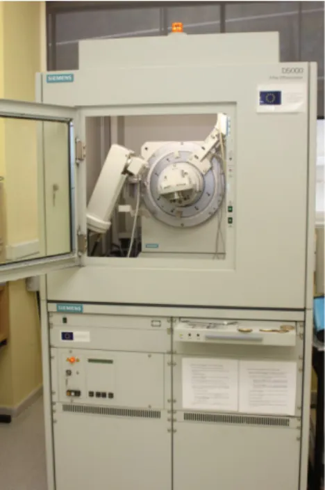
Due to the small time of analysis and sample size, as well as the fact that both bulk and deposited samples could be analyzed, the XRPD technique was used for the characteriza-tion of all samples. Since XR diffraccharacteriza-tion patterns were obtained for both the reagents and the products, the different impurities could also be identified. The instrument used was the diffractometer D5000 SIEMENS from the SAI (Servicios de Apoio a Investigación), shown in Figure 5.128.
The theoretical basis for the XR-diffraction is explained by the Bragg’s law, which is schematized in Figure 5.2. The diffraction is considered as simulta-neous reflections of the X-ray beams by various lattice planes belonging to the same family (or more appropriately, by the atoms lying in those planes). In the figure, θ is the angle between the
prima-Figure 5.1
XR-diffractometer
Figure 5.2
Bragg’s law diagram
ry beam and the planes. The difference in the length of the path of the beams scattered at points B versus those scattered at D equals:
𝐴𝐴𝐴𝐴
����+𝐴𝐴𝐵𝐵���� = 2𝑑𝑑 𝑠𝑠𝑠𝑠𝑠𝑠 𝜃𝜃
If that magnitude is a multiple of the wavelength of the X-rays beams, λ, then the beams will be in phase, leading to maximum positive interference. Otherwise, the beams will can-cel each other through destructive interference.
A XR-diffractometer is able to launch an X-ray beam at different angles at the sample, and then detect the scattered rays. The intensity of the rays is usually represented versus 2θ. The corresponding peaks depend on the position of the crystal planes, and are unique for each structure. It is possible, using advanced techniques, to determine the actual structure of the compound from the scattering data, but that remains outside the scope of this disserta-tion.
5.2 Scanning electron microscopy (SEM)
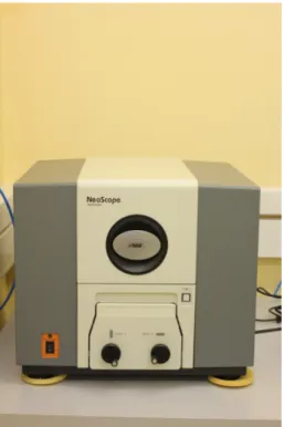
The scanning electron microscopy was a key technique in analyzing the morphology of the thin films and thus determining whether a proper homogeneous film had been obtained. Consequently almost all films were ob-served in the SEM. The instrument employed was a benchtop SEM, model JMC-5000 NeoScope, shown in
Figure 5.329
.
5.2.1 Fundaments30
The scanning electron microscopy is based in the inter-action of an electron beam with the surface of the sam-ple. These interactions can be classified in elastic colli-sions, in which only the trajectory of the colliding
elec-Figure 5.3
Employed SEM
tron is changed, and inelastic collisions, in which part of the energy of the electron is trans-ferred to the solid. The electrons suffer numerous collisions as they advance through the sample, constantly changing directions, which eventually causes most of them of leave the sample as back-scattered electrons (BSE). The resulting beam of back-scattered electrons has a wider angle than the original beam.
Some of the electrons, however, can lose some energy through inelastic collisions. That energy is transferred to the sample, and can cause electrons with energy less than 50 eV to be emitted from the sample itself, together with some X-ray radiation. The emitted elec-trons are called secondary elecelec-trons, and the resulting beam is no much wider than the orig-inal beam. For this reason, the secondary electrons are the most commonly used in the SEM technique; though the back-scattered electrons can also be analyzed, as well as the resulting X-rays30. Those X-rays have a unique energy for each element, and their analysis can give qualitative and quantitative infor-mation in the sample, using the En-ergy-dispersive X-ray spectroscopy (EDX) technique.
5.2.2 Instrument31
The parts of an SEM are summa-rized in Figure 5.4, and are as fol-lows:
1. Electron gun: It creates the electron beam. The electrons them-selves are generated in a filament (such a heated tungsten wire, though other materials can be used) and then they are accelerated by the voltage between the filament (cathode) and
Figure 5.4
Parts of a Scanning Electron Microscopy
an anode.
2. Condenser lens: They are a set of magnetic lens that focus and regulates the electron beam coming from the electron gun.
3. Scanning coils: Also known as deflector plates, they change the direction of the electron beam in the x and y axis, allowing it to scan a rectangular area of the sam-ple surface.
4. Objective lens: As the last set of lens before the sample they bring the electron beam into focus.
5. Specimen holder: It keeps the sample in place and allows it to be moved in the x and
y directions (in the sample plane) as well as in the z direction (specimen height). 6. Secondary electron detector (SED: It collects the secondary electrons coming from
the sample to give a topographical image. Since the secondary electrons usually have low energy, a positive bias is applied to a cage in front of the detector, which directs the electrons into the detector itself.
7. Vacuum pump: To reduce the scattering of the electron beam before reaching the sample is necessary to work in a vacuum. To that end, a vacuum pump is fitted to the system.
5.3 Particle size measurement30
The most common technique for measuring the particle size of a sample is the dynamic light scattering technique (DLS). This technique is based in the Doppler widening of the Rayleigh dispersed light as a result of Brownian motion. In macromolecular solutions, the width of the Reyleigth line correlates to the diffusion coefficient, DT. For a spherical
parti-cle DT is also related to the hydrodynamic diameter, dH, following the Stokes-Einstein
rela-tionship. It should be noted that many other factors, such as the temperature of the sample and its viscosity also take part in the measurement, so they must be known and controlled.
The parts of a DLS instrument are shown in the Figure 5.5, and are as follows:
1. Laser: In the used instrument, this was a red diode laser of a nominal wavelength of 640 nm. It provides the source of light that is scattered by the sample.
2. Lenses: They focus first the light coming from the laser into the sample, and then the dispersed light into the detector.
3. Sample cell: They are either plas-tic or quartz cells, square or cylin-drical. They can hold up to 4 mL of sample.
4. Detector: A photomultiplier tube that converts the light signal com-ing from the sample into an elec-tric signal.
5. Signal processing: Processes the
electric signal into the data that is displayed in the computer.
The letter θ represents the scattering angle at which the scattered light is measured. In most cases, as well as in the used instrument, it equals 90°.
The instrument at our disposal was a 90Plus/BI-MAS, Multi Angle Particle Sizing Option, from Brookhaven Instruments Corporation. For the measurements to be reproducible, they had to be put in an ultrasonic bath for five minutes. After approximately one minute for stabilization the samples were put in cylindrical quartz cells (the plastic cells provided by the manufacturer could not be use since our solvent, THF, attacked the plastic) and intro-duced in the apparatus.
5.4 UV-Visible
To measure the optical properties the V650 UV-Vis Spectophotomer was employed. The measuring of the solid samples, such as the thin films was possible using a 60 mm integrat-ing sphere. The software provided with the equipment also made possible the calculation of the band gap of the compounds. This was employed using the Tauc plot, which represents
Figure 5.5
Parts of a DLS instrument
the αhν1/r value, where α is the absorption coefficient and r depends on the nature of the transition, against the hν value. The lineal range of the plot is where absorption takes place and extrapolating to the x-axis allows the value of the band gap to be calculated.
6
RESULTS AND DISCUSSION
The following section will be focused in the properties of the synthetized DMAPbI3 in
rela-tion to its applicarela-tion in solar cells. The use of additives to achieve good thin film morphol-ogy, especially in changing the particle size of the precursor solutions will be studied as well.
6.1 Properties of the DMAPbI3
As it was mentioned before, the literature concerning the DMAPbI3 was somewhat lacking.
Therefore, much of the groundwork had to be done either by ourselves or by our laboratory companions.
A crucial step was determining the structure of the compound. It was speculated that it would have a perovskite structure similar to the MAPbI3, but as it was later proved, this
was only partially true. A single crystal of DMAPbI3 was successfully synthetized by
dis-solving it in THF, and then slowly evaporating the solvent. The resulting crystal was ana-lyzed by the X-ray single crystal diffraction technique, and the obtained data was used to predict the structure of the compound. This was not done by us, but our laboratory partners, who then provided us with the crystal structure of DMAPbI3
6.1.1 Crystal structure and XRPD
The obtained structure can be seen in Figure 6.1. As it can be observed, it is not a proper perovskite (compare with Figure 2.8): The BX6 octahedra do not share just one vertex with
the neighboring octahedra, but a whole face. Furthermore, they only share it with the octa-hedra directly above and below (c direction), but no with those on the sides (a and b direc-tions). This distortion of the perovskite structure is due to a larger tolerance factor, t, caused by the bigger size of the DMA ion in comparison with the MA ion. The structure loses symmetry as the octahedra are less connected.
Figure 6.1
Different views of the structure of DMAPbI3
Furthermore, the cubic unit cell is lost and substituted by a hexagonal one, making the compound to be known as a hexagonal perovskite.
The XR-diffraction pattern was obtained for the bulk synthetized DMAPbI3, as indicated
before, and compared with the theoretical pattern for the crystal structure of the single crys-tal, as shown in Figure 6.2. As can clearly be seen, the two patterns are very similar, show-ing that the perovskite was successfully synthetized almost without impurities.
Figure 6.2
The XR-diffraction pattern of DMAPbI3
6.1.2 Optical properties
Using a 60 mm integrating sphere, the UV-Vis spectra of the DMAPbI3 was obtained, and
it is shown in Figure 6.3, superimposed with the range of the visible spectrum and the spec-tra from the MAPbI3. For a material to be a good photovoltaic material it is necessary that it
absorbs in the region of the visible spectrum and the near infrared (λ>700 nm). Unfortu-nately, as it can clearly be seen, the DMAPbI3 does not absorb in those wavelengths, which
also explains the lack of color in the prepared films. The only relevant absorption of the material takes place in the ultraviolet region, where little radiation comes from the sun. Fur-thermore, the electronic band gap of the compound was calculated based on the above data to be 2.81 eV, using a Tauc plot. This further limits the uses of the DMAPbI3 as a
photovol-taic material. The band gap is too high to be a proper semiconductor and is also too high to be overcome by the absorbed photons.
In contrast, the MAPbI3 is capable of absorbing both in the visible spectrum and in the near
Figure6.3
The absortion spectrum of the DMAPbI3
infrared, as is also shown in the graph. Also, its bandgap is a more appropriate 1.57 eV, according to the data we obtained using the same procedure as for the DMAPbI3.
However, the band gap of 2.81 eV and the absorption near the ultraviolet spectrum raises the possibility of using the DMAPbI3 as the basis of a blue LED. This could lead an
im-portant revolution in terms cheap light sources with high efficiencies.
6.2 DMAPbI3 thin films
As was previously described (page 25), several thin films of DMAPbI3 were prepared using
either the one or the two-step spin-coating deposition technique. Furthermore, three films were prepared using a mixture of DMAI, MAI, MACl and DMACl; together with PbI3. The
resulting films were analyzed by XRPR and observed under the SEM.
6.2.1 One-step technique
Using the 1-step spin-coating technique a thin film of DMAPbI3 was successfully
deposit-ed. It should be noted, however, that while in the case of the MAPbI3 thin films a dramatic
change of color was observed after the thermal treatment, there was no such change in the case of the DMAPbI3. This lead to some doubts regarding the success of the deposition, but
a closer look to the resulting XR-diffraction patterns proved otherwise.
The obtained pattern is shown in Figure 6.4, superimposed with the theoretical pattern shown before. As it can be seen, there is a very good correlation, proving that the DMAPbI3
was indeed formed. The only exception is the peak at 2θ=12.7°, shown with more detail in
Figure6.5, which is due to leftover impurities of PbI2.
It can also be observed that no all peaks from the theoretical pattern are present in the em-pirical one. This indicates that growth only occurs in some directions, while in others there is almost no growth.
Figure6.5
The XR-diffraction pattern of a thin film of DMAPbI3
Detail of the XR-diffraction pattern of a thin film of DMAPbI3
Figure 6.4
This is further corroborated by the images obtained by the SEM. As shown in Figure 6.6, the DMAPbI3 does not form a homogeneous layer, but instead grows in the form of small
needle-like structures. When the thin film of MAPbI3 was synthetized the same needle-like
structures were observed, although the tended to be bigger and better formed. This mor-phology was believed to be due to a high particle size of the precursor solutions, which seemed to be confirmed when the particle size could not be measured due to being outside the range of the instrument.
6.2.2 Two step technique
The deposition of another thin film of DMAPbI3 layer was also attempted using the
two-step technique. However, this was not successful, as was observed during the experiment, since no thin film seemed to be deposited. Regardless, the sample was analyzed by XRPR; and the resulting pattern is shown in Figure 6.7, once again superimposed with the theoreti-cal pattern. In the inset in the figure it can be seen that, although some DMAPbI3 was
formed, there were large quantities of PbI2 left. Furthermore, the low signal/noise
relation-ship indi cates that almost no product was left in the substrate. For these reasons, this film was not observed under the SEM.
Morphology of the DMAPbI3 thin film
Figure 6.6
6.3 MACl as an additive in MAPbI3 precursor solutions
The failure to deposit thin films with a proper morphology led to the study of the influence of additives in achieve the right morphology. This was first attempted with the MAPbI3
films, since their deposition was better optimized than the DMAPbI3.
Figure6.7
The XR-diffraction pattern of DMAPbI3
6.3.1 Particle size of the precursor solutions
It was reported that, against what was initially believed, the precursor solutions were not perfect solutions, but colloidal suspensions26. This could be easily proved by observing the light dispersion due to the Tyndall effect of a laser beam passing through the solutions, as shown in Figure 6.8.When the laser beams passes through one of the solutions it is clearly visible. For comparison, it can be seen that no such thing happens when the laser passes through distilled water.
The particle size of the solutions with varying amounts of Chloride was measured, and the results for the four solutions are shown in Figure 6.9. The numbers X-1-1 refer to the molar ratios of MACl, MAI and PbI3 respectively. It can be seen that the amount of chloride has a
clear and direct influence in the particle size of the solutions, as the sizes of the particles decrease as the amount of chloride present increases.
Tyndall effect in the precursor solutions
Figure 6.8
Particle size measuraments
Figure 6.9
Relationship between particle size and MACl content
Figure 6.10
This can more clearly be seen in Figure 6.10 where a linear correlation is observed between the MACl content and the most common size of the particles (peaks in the size distribution graph). An explanation of this effect was proposed by Keyou Yan et al.26:
- The PbI2 crystallizes in a trigonal space group, with stacked planes made of [PbI6]
octahedra along the c-direction. While the bonds within the planes are strong chem-ical bonds, the bonds between the planes are only weak Van der Waals forces.
- When in the PbI2 is dissolved in DMF, the solvent is capable of breaking the weak
bonds between the planes. Complete dissolution of the PbI2 is achieved when also a
few of the chemical bonds inside the planes are also broken.
- The organic compounds, CH3NH3X, are able to act as surfactants and to coordinate
to the breakaway planes of PbI2. As the organic component increases by adding
MACl the dissolved PbI2 is further stabilized.
- Higher concentrations of MACl allow for further dissolution of PbI2, which losses
its trigonal structure to enter a quasi-tetragonal soft framework more resembling the perovskite.
6.3.2 Influences in thin film morphology
It was also believed that the change in particle size of the precursor solutions could affect the final morphology of the thin films. To that end, thin films were prepared form each of the precursor solutions using the one-step deposition technique. The resulting films were observed under the SEM, and the resulting images are shown in Figure 6.11. As can be seen, higher amounts of chloride and therefore lower particle sizes led to a loss of the nee-dle-like morphology towards a more homogeneous film. As explained earlier, this is due to the surfactant effect of the organic component of the precursor, which stabilizes a coordina-tion complex for the PbI2 in solution more resembling the final perovskite, avoiding the
formation of needle structures. However, in most of the thin films the substrate was not properly covered, and the morphology was still not perfectly homogeneous, so some more optimization still has to be done.
6.3.3 Presence of Chloride
A final question that was answered was whether the Chloride itself would enter into the perovskite structure as an impurity or it would simply be eliminated during the thermal treatment. To that end, the thin films were analyzed using the Energy-dispersive X-ray spectroscopy (EDX) technique incorporated into the SEM that was being employed. This technique allows the X-rays generated by the electron beam interacting with the sample to be analyzed. Since each element emits X-rays of a specific energy, the technique allows individual elements to be identified within a sample. Also, an estimate of the concentration of the elements can also be obtained.
Figure 6.11
SEM images of thin films with X-1-1 MACl:MAI:PbI2
Figure 6.12
EDX spectra of the thin films
The results of this technique applied to the samples are shown in Figure 6.12. Only in the films with higher starting amount of chloride (1.5-1-1 and 2-1-1films) was present any chloride, and even so in small amounts. Regardless, it was proved that chloride is capable of entering the structure of thee perovskite.
It should also be noted that this small presence of chloride did not dramatically changed the optical properties of the compound. The electronic band gap was measured for those thin films, and the results are 1.60 eV for those films apparently without Cl (0.5-1-1 and 1-1-1 films) and 1.63 for those with small amounts of Cl (1.5-1-1 and 2-1-1 films). The introduc-tion of small amounts of chloride could lead to a better fine-tuning of the perovskite, keep-ing its photovoltaic properties.
6.4 DMAX and MAX as additives in DMAPbI3 precursor solutions
Since the particle size of the DMAPbI3 precursor solution could not be measured, probably
because it being too large and falling outside the range of the instrument, it was decided to use DMACl, MAI and MACl to reduce it.
6.4.1 Change in particle size
As can be seen in Figure 6.13, the particle size was successfully reduced, although not as much as when using MACl as additive. This could be blamed on the presence of DMA, which seems to be a worse surfactant than the MA. The size reduction is similar for all three samples, with the exception of the MACl:DMAI 1:1.5 solution, which has a larger particle size. These results support the theory explained above that is the organic com-pounds that act as a surfactant and help dissolve the PbI2, since the size reduction still takes
place, regardless of the organic compound used as additive. Despite this, the exact nature of the organic compound still has some effect, as well as the presence or absence of chloride.
Figure6.14
The XR-diffraction pattern of the MAI/DMACl,
DMAI/DMACl and the MACl/DMAI thin films
Figure 6.13
Particle size of the DMAX solutions
6.4.2 Thin films
To check the effectiveness of using the additives, the precursor solutions were deposited. The films were sent to XRPR; and the resulting XR-diffraction patterns are shown in Figure
6.14. Despite the somewhat different composition, all three samples have a strong peak at
2θ=11°. Only in the case DMAI/DMACl mixture is the peak a little offset. A closer look to that region, as in Figure 6.15, reveals that despite the presence of MA, sometimes in higher quantities, the compound retains the hexagonal perovskite crystal structure of the DMAPbI3, instead of that of the MAPbI3. This proves that MAX compounds can be used as
additives in the preparation of DMAPbI3 thin films, but not the other way around, since the
compound formed will be DMAPbI3. It should also be noted that the thin films obtained
using additives are much pure than without them, as almost no PbI2 impurities are left.
Once again, this indicates a better solving of the PbI2.
Figure6.13
Detail of the XR-diffraction pattern of the DMACl/MAI sample
Finally, the SEM images obtained of the thin films, shown in Figure 6.16, proved that the additives were successful in avoiding the needle-like morphology, obtaining a more ho-mogenous one. However, a good covering of the substrate was still not achieved, demon-strating the need for further optimization of the process.
Figure 6.14
SEM images of the different thin films
7
CONCLUSIONS
7.1 English
Taking into account the above results and the accompanying discussion the following con-clusions can be reached:
- The DMAPbI3 was successfully obtained by first time in bulk by mixing the
rea-gents, DMAI and PbI2, a very simple method. Its crystal structure was proved to be
that of a hexagonal perovskite. Comparison of its XR-diffraction pattern with its theoretical one proved beyond any doubt that the compound had been formed as a single phase.
- The optical properties of the DMAPbI3 made it unsuitable for photovoltaic use,
alt-hough the very same properties made it an interesting material for a blue LED de-sign.
- A thin film of DMAPbI3 was successfully synthetized by the one-step technique,.
However, the obtained SEM images showed a non-homogeneous needle-like mor-phology.
- The thin film prepared by the two-step technique was also unsuitable for photovol-taic use. While small amounts of the perovskite were synthetized, there were still PbI2 impurities and the substrate was only partially covered.
- When using the one or two steps techniques the thin films had large PbI2 impurities.
Those were avoided, however, when additives were employed.
- It was proved that the MACl could be successfully used as an additive to the precur-sor solutions of MAPbI3. Those were indeed proven to be colloidal solutions by
ob-serving the Tyndall effect. Furthermore, it was shown that the size of those colloids was in clear inverse relationship with the amount of MACl in the solution. This was explained by the surfactant effect of the organic compounds in the solution.
- MAX and DMAX compounds could also be successfully used as additives to the DMAPbI3 precursor solutions. They managed to reduce the particle size of the
tions, while the DMAPbI3 crystal structure remained in the deposited films with
higher purity, despite the presence of MA.
- The particle size of the solutions also had an impact in the final morphology of the thin films. Better, more homogenous morphologies were obtained with smaller par-ticle sizes. Also, it was proved that small amounts of chloride were capable of enter-ing the perovskite structure.