Growth and optical characterization of strain-engineered semiconductor nanostructures
156
0
0
Texto completo
(2) Growth and Optical Characterization of Strain-Engineered Semiconductor Nanostructures. Alessandro Bernardi. Director: Dr. Maria Isabel Alonso Co-director: Prof. Alejandro R. Goñi Tutor: Prof. Jordi Pascual. PhD Thesis Doctorado en Ciencia de Materiales Departamento de Física 2015.
(3)
(4) Ai miei genitori.
(5)
(6) Abstract In this work we explored different pathways to exploit the strain stored into nanoscale layers of materials as a driving force to self-assemble 3D structures. In particular, we have studied the epitaxial growth of self-assembled Ge quantum dots when a submonolayer of carbon is deposited prior to the growth of the dots. Using atomic-force microscopy combined with RHEED and optical techniques like Raman scattering and ellipsometry, we performed a systematic study of the role played by thermally activated Si interdiffusion and the composition of the wetting layer on dot density and morphology. The results give experimental evidence of a kinetically limited growth mechanism in which Ge adatom mobility is determined by chemical interactions among C, Si, and Ge. We suggest a two-stage growth procedure for fine-tuning the dot topography (density, shape and size), useful for possible optoelectronic applications. Moreover we investigated the dynamics of strain relaxation during the capping of islands, which is useful for engineering devices based on multistacks of quantum dots. We also analysed the evolution of Ge nanostructures grown by combining nanostenciling and pulsed laser deposition, as a promising approach for the parallel patterning of semiconductor nanostructures for optoelectronics. Apart from the growth of 3D islands, we applied strain-driven engineering to release rolled-up microtubes, obtained from strained semiconductor heterostructures. Through micro-Raman spectroscopy we were able to determine the residual strain, which results in a frequency shift of phonon modes measured on the tube as compared with reference unstrained material. We developed a simple elastic model to describe the measured phonon-frequency shifts, from which we estimate the strain status of the microtube. Results demonstrate the power of Raman spectroscopy as a diagnostic tool for engineering of strain-driven self-positioning microelectromechanical systems. We tested the potential application of this rolled-up nanotechnology to obtain a lab-in-a-tube device where light is used as a biochemical sensor. We fabricated rolled up microtubes consisting of Si/SiOx integrated on a Si chip and we analysed their properties to use them as a refractometric sensor. An aqueous sugar solution was inserted into the microtube, which leads to a change in refractive index and, as a result, to a detectable spectral shift of the whispering gallery modes. This prototype proved that the monolithic on-chip integration of strain-engineered microtubes is a promising approach to design optofluidic channels for lab-on-achip applications.. 3.
(7)
(8) Contents 1. Introduction ..................................................................................................................... 7. 2. Results and Discussion ................................................................................................. 9 2.1. Self-assembling of Carbon-induced Germanium quantum dots ......................... 9. 2.1.1. Effect of silicon interdiffusion on thermally activated wetting layers ................ 10. 2.1.2. Growth dynamics on SiGe strained layers and fine tuning of island density ... 11. 2.1.3. Morphology, strain and composition during capping of dots ................................. 13. COMPENDIUM ARTICLES .................................................................................................................................. 17. 2.2. Growth and characterization of SiGe nanostructures ..........................................19. 2.2.1. Raman characterization of SiGe dots under high pressure ..................................... 19. CORE RESEARCH ARTICLES ............................................................................................................................. 21. 2.2.2. SiGe alloys: measurement of phonon strain-shift coefficients ............................... 23. COMPLEMENTARY ARTICLES ......................................................................................................................... 25. 2.2.3. Multilayers of Ge quantum dots ........................................................................................... 27. COMPLEMENTARY ARTICLES ......................................................................................................................... 29. 2.2.4. Ge nanostructures via PLD nanostencilling .................................................................... 31. CORE RESEARCH ARTICLE ............................................................................................................................... 33 COMPLEMENTARY ARTICLE............................................................................................................................ 35. 2.2.5. Optical characterization of Ge nanocrystals ................................................................... 37. COMPLEMENTARY ARTICLES ......................................................................................................................... 39. 2.3. Rolled-up semiconductor microtubes .......................................................................41. 2.3.1. Probing strain in microtubes by micro-Raman spectroscopy ................................ 42. 2.3.2. Lab-in-a-tube: on-chip integration of an optical ring resonator for biochemical. sensing............................................................................................................................................................ 44 CORE RESEARCH ARTICLES ............................................................................................................................. 47. 3. Conclusions ................................................................................................................... 49. 4. References ..................................................................................................................... 53. 5. Acknowledgements .................................................................................................... 55. 5.
(9)
(10) 1 Introduction Before you start reading this thesis, could you please raise your head for a second and take a look around you? There must be somebody typing on his last generation smartphone to send messages to the world at an incomparable speed of data processing. Samsung just unveiled [1] its 14-nanometer chipset powering the new Galaxy S6 that it said offers better battery life and performance. When compared to Samsung's 20-nanometer process technology, the new 14-nanometer process enables up to 20 percent higher speed, 35 percent less power consumption and 30 percent productivity gain. We already have now in the market, as an industry standard, a nanoscale technology that at the beginning of this thesis appeared to be futuristic but that has been evolving pretty fast, in fact. In order to optimize production and scale devices to match the market requirements, the semiconductor engineers require deep know-how on surface science and ways to manipulate and characterize materials with nanometric precision. The core research of this work focuses on self-assembling of strain-engineered semiconductor nanostructures, i.e. controlling the amount of strain stored in the materials as a driving force to release 3D structures, with the challenge to manipulate their positioning and direct integration on a chip. In addition to the bottom-up techniques, this thesis is highly oriented to the optical characterization and development of phenomenological models. The optical characterization is used at first as a way to investigate the chemical composition and the strain distribution inside of the nanostructured systems. We demonstrate how optical mapping can be an excellent non-invasive probing tool to test integrated nanostructured semiconductor devices, as recently reported also for mapping of SiGe nanowires [2]. On the other hand, once a strain-engineered nanostructured device is fabricated, detectable variations of its optical properties can easily reveal subtle changes of the boundary conditions, making it possible to assemble a miniaturized sensor integrated on a semiconductor chip: a prototype of a so called Lab-on-a-chip. In the next chapter of results and discussion, the papers published by the author of this thesis are organized in different thematic sections, covering the different areas of research and dealing with different types of strain-engineered nanostructured systems. The core of the thesis deals with self-assembling of carbon induced Ge quantum dots by molecular beam epitaxy (2.1). Besides optimizing the preparation of materials, the growth dynamics have been investigated by in situ RHEED1 and the. 1. Reflection High Energy Electron Diffraction 7.
(11) resulting morphology of nanostructures has been probed by AFM2. The use of impurities and stressors later inspired the work of some other research groups focusing on ordering of SiGe islands [3,4] and our results were presented in some recent reports on self-assembling of SiGe nanostructures [5,6]. The same growth technique, Molecular Beam Epitaxy, is used to deposit strained semiconductor multilayers that have been processed to release freestanding microtubes [7], with potential application as microfluidic devices and optical resonators (2.3). After our first prototype, the fabrication process evolved to permit the preparation of large arrays of multifunctional microtubes [8] and several futuristic applications of labin-a-tube [9,10,11,12,13,14] were discussed. Apart from the strain-engineered processing, the optical characterization (mainly Raman Spectroscopy) of the microtubes is also an important contribution to this thesis work. Our original approach, combining elastic models with the phonon strain-shift theory, has been reviewed as a technique to study the mechanical behaviour of microdevices [15] and nanostructures [16,17,18,19,20,21]. Elastic strain plays a key role in the growth dynamics and optical properties of a number of other semiconductor nanostructures, which have been fabricated or characterized as a result of different collaborations, emerged during this thesis. Defining good measurement protocols for the determination of strain and composition of SiGe nanostructures was crucial for this work and it has been still a challenge in several other experiments following up [22]. Our results provide useful insights for potential application in optoelectronic and nanocalorimetry of some interesting strain-engineered semiconductor nanostructures, ranging from strained epitaxial SiGe alloys (2.2.2), multistacks of quantum dots (1.1.1), Ge nanostructures on patterned substrates (2.2.4) and crystallized Ge nanocrystals (2.2.5). Within the different works presented, there is a hierarchy that can be summarized like this: A. COMPENDIUM ARTICLES: work officially presented for this thesis and approved by the scientific doctorate committee to be the constituent of the compendium. B. CORE RESEARCH ARTICLES: papers collecting the main results of the research conducted during the doctorate, directly related with the compendium articles and in which the author of this thesis has a leading role conducting experiments and discussing results. C. COMPLEMENTARY ARTICLES: other works which are fruit of different scientific collaborations in which the author of this thesis has a secondary role, generally restricted to the growth and optical characterization of samples.. 2. 8. Atomic Force Microscopy.
(12) 2 Results and Discussion 2.1 Self-assembling of Carbon-induced Germanium quantum dots Size, density, shape uniformity, and ordering of quantum dots QDs are crucial parameters when self-assembling is considered for applications in optoelectronic devices. In recent years, different smart strategies have been proposed to address the problem of dot engineering. Increase of dot density at very low substrate temperatures and/or high deposition rates is a well-established technique but in most cases it is not of practical interest for applications due to the degradation of crystalline quality. Perfect position control keeping high quality of dot ensembles can be achieved by means of artificially nanopatterned substrates. This approach is, however, less suitable for potential high surface and low cost applications. An alternative are spontaneous bottom up approaches such as the use of template layers to guide the selective nucleation of dots, which has demonstrated to be a good method to control the positioning of dots by inducing self-ordering processes during growth. A strain-driven instability in SiGe/Si(001) pseudomorphic layers leads to the formation of periodic surface undulations ripples acting as a natural template pattern that can be controlled by thickness, composition, and selection of vicinal Si(001) surfaces. Other routes include Ge deposition on relaxed SiGe/Si buffer layers and deposition on buried dislocation networks. Another relevant bottom up strategy towards efficient dot engineering involves surface modification through deposition of sub monolayer amounts of impurities that can reduce the diffusion length i.e., enhancing dot density and altering the energetics of nucleation. In this work we focused our attention on the growth of carbon-induced QDs, getting insight into the surface processes which are relevant at the stage of island nucleation. Up to now the C-induced growth of Ge quantum dots (C-QDs) has been discussed in terms of a single-stage process determined by growth parameters like substrate temperature and amount of C. In that way, it is not possible to experimentally decouple different phenomena that take place at the same time, namely silicon incorporation in the QDs and kinetic aspects of the 3D growth. Here we aimed at putting in evidence the previously ignored role of silicon interdiffusion. Based on experimental observation we propose a mechanism of growth where enhanced lattice mismatch, limited kinetic conditions and chemical interaction altogether contribute to complete an overall picture of the processes involved in C-induced growth. In order to fully understand the growth dynamics we present results grouped in three scenarios: •. Self-assembling of dots on top of Ge wetting layers (WLs) grown at different temperatures, where the intermixing with the silicon substrate plays a crucial role (2.1.1).. 9.
(13) •. Growth of dots on top of strained SiGe layers of different composition. This case is somehow reproducing conditions similar to those of the deposition on top of an intermixed WL, but with the possibility to better control the chemistry at the surface. This approach represents a possible strategy for engineering and tuning dots size and density (2.1.2).. •. Capping Ge dots with silicon affects the chemical composition of the islands and their strain status. On one side we follow the pathway of strainrelaxation driving the self-assembling of dots (with and without carbon) and on the other side, after capping, we observe partial recompression and variable silicon interdiffusion depending on the morphological characteristics of the islands. 3D growth and silicon intermixing are competitive mechanisms to relief the built-in strain and our results shed some light on how to engineer capped dot devices and multistacks of strained nanostructures (2.1.3).. 2.1.1 Effect of silicon interdiffusion on thermally activated wetting layers A set of samples was prepared by solid-source molecular beam epitaxy, always according to the following procedure: after oxide desorption at 900 ºC and 50 nm thick Si buffer layer deposition, a 3.7 Å thick Ge WL was grown at given fixed temperature TWL ranging from 330 to 750 ºC. Subsequently, the temperature was stabilized to 500 ºC before depositing 0.1 monolayers (MLs) of carbon from a calibrated sublimation filament. Finally, keeping the temperature fixed at 500 ºC for all samples, a top 5.8 Å thick layer of Ge was grown, leading to almost instantaneous formation of self-assembled C-QDs without reaching the typical critical thickness for the conventional 2D–3D growth mode transition which occurs in the absence of carbon. The growth was monitored in situ by RHEED and the island topography was studied ex situ by AFM. In order to evaluate the composition and residual strain, samples were characterized by optical measurements at room temperature. Raman spectroscopy was carried out with the 514.5 nm line of an Ar-ion laser for excitation. Light was focused onto the sample with a spot size of about 1 μm and a laser power of 4 mW. In order to suppress contributions from second-order processes, we used the scattering geometry ! !" !, where x, y and z are the [100], [010] and [001] crystallographic directions, respectively. The ellipsometric spectra were collected using a rotating polarizer ellipsometer in the 1.4–4.8 eV spectral range. The main original results of this work can be summarized in the following points: •. 10. Increasing only the deposition temperature of the Ge WL leads to gradually higher QD densities, in apparent contradiction with what is well established in literature, where maximum dot densities are generally obtained in low growth temperature processes.
(14) •. Since we kept the substrate temperature always fixed to 500 ºC during the QD nucleation stage, we exclude any Arrhenius-type of kinetic dependence on temperature of Ge adatom mobility. Then, the observed topography strictly reflects the intrinsic characteristics of the surface material. A change in the growth temperature during the WL deposition can be related to the amount of silicon incorporated in the Ge overlayers.. •. Data obtained from Raman and spectroscopic ellipsometry are consistent: the material constituting the QDs is nearly pure Ge and the amount of silicon intermixed in the islands goes up to 10% when increasing the TWL from 330 ºC to 750 ºC. For the highest temperature we estimate a large Si content in the WL, around 75%.. •. A clear correlation between topographic features and Si intermixing can be inferred. Increasing temperature favours Si interdiffusion in the nominally pure Ge WL and eventually in the QD layer, until a saturation value is reached due to Ge overgrowth. The QD density follows the same trend with a maximum saturation density in this experiment one order of magnitude lower (8.0 ×10⁹ islands/cm2) than for growth of C-QDs on bare Si(001).. •. The presence of a certain amount of Si in the WL due to thermally activated interdiffusion could contribute to partially stabilize carbon on top surface layers, considering that Si–C bonds are much more stable than Ge–C ones. From this perspective a higher growth temperature TWL means a higher Si content in the WL. Consequently, C can arrange in metastable surface reconstruction patches, which are responsible for the decrease of adatom mobility, thus explaining the observed increase in dot density.. •. By close inspection of the C-QD topography we found out that even the smallest islands are all dome-shaped with no evidence of flatter pyramidlike dots (with aspect ratio <0.10). The main effect of carbon predeposition is to shrink the in-plane lattice parameter because of C-rich patches formed on the surface. The resulting enhancement of the lattice mismatch is responsible for the growth-mode change from Stranski–Krastanow to Volmer–Weber. In fact, our RHEED observations suggest the onset of islanding when we start Ge growth immediately after the C-submonolayer deposition, even if the WL thickness is subcritical.. •. The presence of carbon also affects the energetics of the pyramid–dome shape transition. The main reason for the reduction of the critical volume for the appearance of dome-shaped islands is the locally enhanced lattice misfit.. 2.1.2 Growth dynamics on SiGe strained layers and fine tuning of island density We present a different route for manipulating Ge island self-assembling based on the combination of epitaxial growth on strained SiGe buffer layers and carbon. 11.
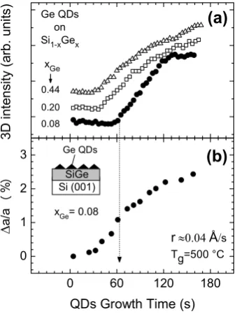
(15) predeposition. Inspired by the results on the influence of Si interdiffusion (2.1.1) and the Ge–C repulsive interaction on the resulting Ge dot topography we make use of the effect that a submonolayer deposition of C has on the Ge adatom diffusion. Our results point to a reduction by two orders of magnitude of dot density with increasing Ge content in the buffer layer. A thin strained Si1−xGex buffer layer with Ge composition (x) ranging from 0% to 60% was deposited on a silicon substrate at 400 °C. For all the samples the SiGe buffer layer thickness remained below the limit of metastability, preventing threedimensional nucleation of SiGe quantum dots, as confirmed by in situ RHEED monitoring. The temperature was then raised and maintained at 500 °C during the deposition of 0.1 ML of carbon by a sublimation filament and the subsequent evaporation of 6 Å of Ge at a fixed growth rate of 0.04 Å/s, leading to selfassembling of quantum dots. The growth was monitored in situ by RHEED using 20 keV electrons and a CCD camera to record the diffraction pattern displayed on a phosphor screen. The main original results of this work can be summarized in the following points:. 12. •. The first striking result of this work concerns the observed tendency of the dot density which exhibits a significant, monotonous decrease by two orders of magnitude with increasing Ge content in the buffer layer from 0% up to 60% whereas the interdot separation (λ) increases. Our results follow a trend which is exactly the opposite of what we could expect if the nucleation of dots was driven by morphological instabilities (ripples) or induced by the average roughness of a Ge rich strained layer. In order to explain our experimental findings we need to take into account the effects of the submonolayer of carbon.. •. We propose a mechanism by which the chemical interactions among Si, Ge, and C drive the growth process. The Si–C attractive interaction favors C condensation, leading to the appearance of c(4×4) reconstruction patches also associated with an enhanced surface roughness. If the carbon is deposited on a layer containing Ge, the Ge–C repulsion induces phase separation and, depending on Ge content, the C-induced reconstruction patches become increasingly fragmented, being the C atoms progressively incorporated at random sites in the film. The key point is that the formation of the reconstruction patches produces a significant quenching of the Ge adatom diffusion, which within the kinetic model implies the self-assembled growth of a high density of Ge dots. With increasing Ge content of the buffer layer the C-induced patches gradually disappear, the surface roughness diminishes, and the Ge adatom diffusivity becomes enhanced, resulting in lower dot densities.. •. The RHEED patterns collected in situ reveal interesting insights about the growth dynamics. Monitoring the intensity of the 3D spotty pattern and simultaneously extracting the distance between streaks (or spots) it is possible to quantify the strain relaxation associated to the dot growth, which appears to take place from the very beginning of the dot growth. The.
(16) evolution of Ge dots on C-alloyed strained SiGe surfaces proceeds via a Volmer-Weber mode, similarly to the case (2.1.1) of C-induced Ge dots on Si(001). •. When the Ge deposition starts we detect a certain delay of time before the appearance of a spotty pattern: this observation is consistent with the estimated critical volume required for RHEED detection of a 3D cluster, in the range of 0.5-7× 10³ nm3 with increasing Ge content in the buffer layer. The obtained values match with the sizes of the smallest dome-shaped islands determined from AFM images.. 2.1.3 Morphology, strain and composition during capping of dots In the present work we describe an experimentally observed growth mode change from Stranski–Krastanow (SK) in the absence of C to Volmer–Weber (VW) when depositing Ge on a C-enriched Si substrate. The evolution of the surface lattice parameter is followed up to large Ge coverage where both elastic and plastic mechanisms of relaxation are active. We also study the process of capping the islands with silicon to understand how it affects the final composition and the elastic recompression of the dots. Finally, we also focus on the structural properties of the cap layer and obtain evidence of the existence of compressive stress induced by local strain fields associated with carbon-rich patches. Samples under investigation were prepared by solid-source molecular beam epitaxy. After oxide desorption at 900 °C and 100 nm thick Si buffer layer deposition, the substrate temperature was set to 500 °C. Subsequently, ∼0.1 monolayers (MLs) of carbon were predeposited on the Si surface from a calibrated sublimation filament. The self-assembling of carbon-induced quantum dots (CQDs) was achieved by evaporation of 12 MLs of Ge. A reference sample was prepared following exactly the same growth procedure as above, but omitting the step of carbon predeposition. As a result standard Stranski–Krastanow quantum dots (SK QDs) were obtained. Finally, part of the surface of the samples was capped with a 10 nm thick Si layer deposited at 300 °C, in order not to alter the shape of buried dots. Growth was monitored in situ by RHEED and the island topography was studied ex situ by AFM. By using complementary surface science tools we were able to study different aspects of the growth of strained Ge/Si islands. RHEED was used to in situ monitor the evolution of the in-plane lattice parameter, allowing us to determine the set in of strain relaxation due to nucleation of 3D clusters. In the absence of C, we observed the formation of a flat 2D wetting layer (WL), taking place before the gain in elastic energy becomes dominant over the energetic term associated with the increase of surface (SK growth). In this case, the first stage of island growth accounts for the relaxation of less than 50% of the lattice mismatch and it can be attributed to the nucleation of small and shallow pyramids. When the islands get bigger, they transform into domes or dislocated Ge clusters that can relax the. 13.
(17) strain more efficiently, so that after 10 MLs of coverage we already measure a lattice parameter approaching the value of bulk Ge. The strain-relaxation pathway changes quite dramatically when carbon is used to engineer the dot topography. In this case, the presence of carbon-rich patches and the repulsive Ge–C interaction prevent the formation of a WL, i.e., it is energetically more convenient to increase the Ge surface with nucleation of 3D clusters, rather than wetting the carbon-alloyed surface. As a result, the lattice parameter relaxation associated with the 3D nucleation can be observed starting from the very first stages of Ge deposition, which is experimental evidence of the growth mode change from Stranski–Krastanow to Volmer–Weber. In the case of C-QDs, we do not observe two regimes of strain relaxation (shallow and steeper islands) but a continuous progressive evolution of the lattice parameter, and this observation is consistent with the AFM topography characterized only by dome-shaped clusters. The density of domes is exceptionally high (∼1011 cm−2) due to reduced mobility of Ge on a roughened carbon-alloyed surface. The reduced surface diffusion that explains the high dot density is likely to be also responsible for the quenching of Si intermixing in the islands. Both island morphology and composition keep evolving while the growth or annealing proceeds. Intermixing dynamics is thought to be dominated by surface rather than bulk diffusion, especially at temperatures below 500 °C. Therefore, it is possible that in the presence of C, the process of Si intermixing is kinetically limited. Then, capped C-QDs are less intermixed and retain larger strain than SK-QDs, as experimentally observed. The limited intermixing as a partial strain-reliever and the presence of local inhomogeneous strain fields are both consistent with the extreme decrease of the critical volume for the pyramid-to-dome transition, to the point where only dome-shaped clusters can be observed. As a result of the deposition of 12 MLs of Ge, the dots completely relax their strain towards their apex, as can be measured by RHEED probing the topmost atomic layers. Raman spectroscopy becomes a useful tool to study instead the average strain distribution inside the volume of the islands. The relevant question arising when evaluating the Raman results is to decide which is the adequate elastic model to describe the strain status of a quantum dot. Once we have measured the LO phonon frequency shift associated with the lattice deformation, in order to quantify the strain, we need to know the relation existing between the in-plane (∈∥ ) and out-of-plane (∈! ) components. A tiny shallow island is somehow similar to a pseudomorphic 2D layer and its strain status is likely described by a biaxial model (i.e., the lattice is compressed in the in-plane direction and it is free to expand in the out-of-plane direction, according to Hooke’s law). For steeper islands embedded in a matrix (capped dots), the strain status of dots can be rather described by a hydrostatic model (∈! = ∈∥ ). •. 14. According to the results the uncapped dots (both SK and C-QDs) retain only between 10% and 30% of the strain, depending on whether we consider a hydrostatic or biaxial model, respectively..
(18) •. After capping with a 10 nm thick Si layer, the islands are recompressed and we can clearly recognize in Raman spectra features corresponding to two contributions from portions of material with different composition and strain. The experimental piece of evidence is that we are probing regions of material with rather different structural properties; thus, it is unlikely that they refer to different portions of the same island. This argument leads us to ascribe the contributions to two separate families of islands: the smaller coherent islands are fully recompressed (according to the biaxial model) whereas the bigger relaxed domes are less affected by the thin cap layer.. •. Raman spectroscopy turns out to be a powerful technique capable of pointing out the presence of local structural inhomogeneities of the quantum dots, complementing the information achieved by RHEED analysis. When probing dot ensembles most of the characterization tools are sensitive to the 3D clusters due to the grazing incidence geometry and shadowing (this is the case of RHEED) or for confinement of carriers in the islands and the absence of a signal collectable from the WL (like in Raman spectroscopy. In this context, ellipsometry provides unique information on the average strain field of the silicon cap layer, which indicates a local compressive strain in the regions between islands associated with the carbon-rich patches.. 15.
(19)
(20) COMPENDIUM ARTICLES. Article n: 1 Authors: A. Bernardi, J. O. Ossó, M. I. Alonso, A. R. Goñi and M. Garriga Title: Influence of Si interdiffusion on carbon-induced growth of Ge quantum dots: a strategy for tuning island density Journal: Nanotechnology Doi: 10.1088/0957-4484/17/10/026. Article n: 2 Authors: A. Bernardi, M. I. Alonso, A. R. Goñi, J. O. Ossó, and M. Garriga Title: Density control on self-assembling of Ge islands using carbon-alloyed strained SiGe layers Journal: Applied Physics Letters Doi: 10.1063/1.2349317. Article n: 3 Authors: A. Bernardi, M.I. Alonso, A.R. Goñi, J.O. Ossó, M. Garriga Title: Growth dynamics of C-induced Ge dots on Si1-xGex strained layers Journal: Surface Science Doi: 10.1016/j.susc.2006.12.048. 17.
(21) Article n: 4 Authors: A. Bernardi, M. I. Alonso, J. S. Reparaz, A. R. Goñi, P. D. Lacharmoise, J. O. Ossó and M. Garriga Title: Evolution of strain and composition during growth and capping of Ge quantum dots with different morphologies Journal: Nanotechnology Doi: 10.1088/0957-4484/18/47/475401. 18.
(22) INSTITUTE OF PHYSICS PUBLISHING. NANOTECHNOLOGY. Nanotechnology 17 (2006) 2602–2608. doi:10.1088/0957-4484/17/10/026. Influence of Si interdiffusion on carbon-induced growth of Ge quantum dots: a strategy for tuning island density A Bernardi, J O Ossó, M I Alonso, A R Goñi1 and M Garriga Institut de Ciència de Materials de Barcelona-CSIC, Esfera UAB, 08193 Bellaterra, Spain E-mail: [email protected]. Received 3 January 2006, in final form 14 February 2006 Published 28 April 2006 Online at stacks.iop.org/Nano/17/2602 Abstract We have studied the epitaxial growth of self-assembled Ge quantum dots when a submonolayer of carbon is deposited on a Ge wetting layer (WL) prior to the growth of the dots. Using atomic-force microscopy combined with optical techniques like Raman and ellipsometry, we performed a systematic study of the role played by thermally activated Si interdiffusion on dot density, composition and morphology, by changing only the growth temperature TWL of the WL. Strikingly, we observe that higher dot densities and a narrower size distribution are achieved by increasing the deposition temperature TWL , i.e. by enhancing Si interdiffusion from the substrate. We suggest a two-stage growth procedure for fine tuning of dot topography (density, shape and size) useful for possible optoelectronic applications.. 1. Introduction Bottom-up approaches for the fabrication of nanostructures have attracted great interest in recent years, appearing as a viable path towards a new generation of nanotechnological devices [1]. Self-assembling of epitaxial germanium quantum dots (QDs) has been extensively studied in the last decade and fundamental physical processes governing heteroepitaxy have been described and modelled elegantly [2]. The next goal will be to attain full capability to tailor material properties and to modify the growth dynamics in order to match specific requirements, depending on the physical process one needs to exploit for a given field of application. In particular, the design of a new class of silicon-based optoelectronic devices [3] requires a high density of QDs with narrow size distribution. However, conventional self-assembling of Ge QDs on Si(001) leads to a bimodal distribution of island shapes and sizes [4, 5]. The addition of impurity atoms has been demonstrated [6–11] to be a valid option for modifying the growth mode and to produce more homogeneous ensembles of islands. Several possible approaches have been explored by various research groups: one well established way for controlling morphology consists in predeposition of a surfactant 1 ICREA Research Professor.. 0957-4484/06/102602+07$30.00. like Sb [6], or alternative dopants like P [7] or B [8]. For instance, predeposition of carbon is an especially successful pathway [9–11]. All these cases share a lot of similarities in the growth dynamics: the addition of extremely low coverages of impurities leads to a significant increase of dot density and consequent reduction of average dot size. Previous experimental work evidenced the role of carbon in terms of reduction of the Ge diffusion length at the substrate surface, which is reflected in the increase of dot density. Direct observation of carbon-induced c(4 × 4) reconstruction on Si(001) surface [12] hints at a selective deposition of Ge in carbon-free regions in agreement with theoretical predictions which consider the repulsive interaction between Ge and C [13]. Carbon has been predeposited both on bare silicon substrates [12] and eventually on Ge wetting layers (WLs) [14], but, besides observing a systematic increase of dot density, no explanation has been yet proposed to understand why the addition of carbon directly to silicon leads to dot densities roughly one order of magnitude higher. Other basic questions on the kinetic evolution and on the thermodynamically favoured equilibrium shape of Cinduced islands remain yet unanswered. In this work we focused our attention on the growth of carbon-induced QDs, getting insight into the surface processes which are relevant at the stage of island nucleation. Up to now the C-induced growth of Ge quantum dots (C-QDs) has. © 2006 IOP Publishing Ltd Printed in the UK. 2602.
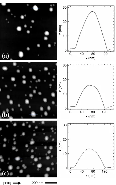
(23) Influence of Si interdiffusion on carbon-induced growth of Ge quantum dots. been discussed in terms of a single-stage process determined by growth parameters like substrate temperature and amount of C [10, 11]. In that way, it is not possible to experimentally decouple different phenomena that take place at the same time, namely silicon incorporation in the QDs and kinetic aspects of the 3D growth. Here we aimed at putting in evidence of the previously ignored role of silicon interdiffusion. Based on experimental observation we propose a mechanism of growth where enhanced lattice mismatch, limited kinetic conditions and chemical interaction altogether contribute to complete an overall picture of the processes involved in C-induced growth. We will show that the density of QDs increases when the WL has a higher Si content due to higher growth temperature TWL . Carbon on a Si-rich surface can arrange in metastable reconstruction patches that reduce the adatom mobility, giving an increase of dot density. On a Ge-rich WL, such as obtained at lower TWL , deposited C tends to be buried into deeper layers and have less influence on the adatom mobility, thus allowing the growth of larger and less dense islands.. 30. z (nm). 20. 0. 3. Results 3.1. Topography by atomic force microscopy Figure 1 shows the topographic images of three representative samples. In all cases the typically observed morphology is that of dome-shaped islands with not clear faceting, in agreement with published work [9–11] on carbon-induced Ge QDs. Nevertheless, quite a surprising behaviour can be pointed out: increasing only the deposition temperature of the Ge WL leads to gradually higher QD densities, in apparent. 0. 40. 80 x (nm). 120. 0. 40. 80 x (nm). 120. 0. 40. 80 x (nm). 120. 30. z (nm). 20. 10. 0. 2. Experimental details. 30. 20 z (nm). A set of samples was prepared by solid-source molecular beam epitaxy, always according to the following procedure: after oxide desorption at 900 ◦ C and 50 nm thick Si buffer layer deposition, a 3.7 Å thick Ge WL was grown at given fixed temperature TWL ranging from 330 to 750 ◦ C. Subsequently, the temperature was stabilized to 500 ◦ C before depositing 0.1 monolayers (MLs) of carbon from a calibrated sublimation filament. Finally, keeping the temperature fixed at 500 ◦ C for all samples, a top 5.8 Å thick layer of Ge was grown, leading to almost instantaneous formation of self-assembled C-QDs without reaching the typical critical thickness for the conventional 2D–3D growth mode transition which occurs in the absence of carbon. The growth was monitored in situ by reflection high energy electron diffraction (RHEED), and the island topography was studied ex situ by atomic force microscopy. In order to evaluate the composition and residual strain, samples were characterized by optical measurements at room temperature. Raman spectroscopy was carried out with the 514.5 nm line of an Ar-ion laser for excitation. Light was focused onto the sample with a spot size of about 1 µm and a laser power of 4 mW. In order to suppress contributions from second-order processes, we used the scattering geometry z(x y)z̄ , where x , y and z are the [100], [010] and [001] crystallographic directions, respectively. The ellipsometric spectra were collected using a rotating polarizer ellipsometer in the 1.4–4.8 eV spectral range.. 10. 10. 0. [110]. 200 nm. Figure 1. Topographic images (1 µm × 1 µm) of C-QDs obtained for different growth temperatures of the wetting layer (WL) at (a) 330 ◦ C, (b) 400 ◦ C and (c) 750 ◦ C. The right-hand panels show representative island profiles of each image. (This figure is in colour only in the electronic version). contradiction with what is well established in literature, where maximum dot densities are generally obtained in low growth temperature processes [11, 14]. Since we kept the substrate temperature always fixed to 500 ◦ C during the QD nucleation stage, we exclude any Arrhenius-type of kinetic dependence on temperature of Ge adatom mobility. Then, the observed topography strictly reflects the intrinsic characteristics of the surface material. A change in the growth temperature during the WL deposition can be related to the amount of silicon incorporated in the Ge overlayers; in order to explain the observed topographic changes, interdiffusion processes need to be taken into account. The questions arising about the correlation of the dot density with the composition of the QDs will be addressed by optical characterization techniques in the following sections. 3.2. Raman spectroscopy Raman spectroscopy has been demonstrated to be a surfacesensitive technique that is useful for extracting information about composition and strain inside the QDs [15]. From the 2603.
(24) A Bernardi et al. Si–Ge peak cannot be resolved, indicating an even higher Ge content in QDs. Therefore, for a quantitative determination of composition from just the Ge–Ge peak an assumption about the strain of the islands is required. Since the measured frequency of the Ge–Ge phonon mode is the same for all the samples (301.3 cm−1 ), our interpretation is that small variations of composition, if any, induce shifts that are easily compensated by slightly different degrees of strain relaxation. Just for an estimation, it is reasonable to expect that for TWL = 330 ◦ C the Si interdiffusion process is completely quenched, i.e. the overgrown QDs are almost of pure Ge. Consequently, evaluating the strain from equation (1), we obtain ϵ∥ ≈ −0.1 ± 0.2%. In other words, bigger islands obtained at lower TWL are found to be more relaxed than smaller domes, in agreement with the expected strain-dependent scaling of QD size [18]. Figure 2. Raman spectra of C-QD samples obtained for different TWL and compared with the spectra of the substrate (dotted line) and a reference sample having only a Ge WL. The fingerprints of the QDs are the Ge–Ge peak at 301.3 cm−1 and a much weaker Si–Ge phonon mode (see the inset). The intensity is normalized to that of the strong Si phonon mode of the substrate. The spectra are vertically shifted for clarity.. Raman spectra shown in figure 2, we can extract the following information.. • Apart from the strong silicon peak at 520.5 cm−1 coming from the LO phonon mode of the substrate, a Ge–Ge vibration peak can be detected at 301.3 cm−1 . In contrast, the spectrum of a reference sample, where only the thin Ge WL at 750 ◦ C was deposited, exhibits a small peak in the 300 cm−1 range, which is attributed because of its shape and intensity to the residual second-order 2TA phonon feature, also detectable in the silicon substrate. We conclude that the Ge–Ge phonon mode observed in the different samples can be ascribed to scattering only from the QDs without contribution of the WLs. • In the 400 cm−1 range, it is possible to resolve a peak at ∼390 cm−1 (see inset to figure 2) for the sample corresponding to the highest temperature (TWL = 750 ◦ C) for the WL growth stage. This peak is attributed to the Si– Ge phonon mode and its presence hints at interdiffusion of silicon through the WL into the QDs. The spectral positions (in cm−1 ) of the Ge–Ge and Si–Ge peaks allow us to extract the composition ( x ) of the Si1−x Gex alloy and the in-plane strain (ϵ∥ ) by applying the empirical relations [15] ωGe–Ge = 284 + 5x + 12x 2 + bGe–Ge ϵ∥ ,. ωSi–Ge = 400 + 29x − 95x 2 + 213x 3 − 170x 4 + bSi–Ge ϵ∥ .. (1) (2). = Using the phonon strain-shift coefficients bGe–Ge −400 cm−1 and bSi–Ge = −575 cm−1 determined by Tan et al [16] for Ge-rich self-assembled QDs, for TWL = 750 ◦ C we obtain from equations (1) and (2) a Ge composition of xGe = 0.94±0.02 and a compressive strain equal to ϵ∥ ≈ −0.5±0.2% (errors are estimated considering the dispersion of strain-shift coefficients found in literature [17]). For TWL < 750 ◦ C, the 2604. • Another remarkable feature of the collected spectra concerns the different intensities of the Ge–Ge peaks, even though the amount of Ge deposited is the same for all the samples. This can be understood by taking into account Raman resonance effects. In fact, the incident laser light has an energy of 2.414 eV quite close to the E 1 electronic interband transition in Si1−x Gex . An increase of Ge content in the islands causes a redshift of the electronic transition with the consequent progressive loss of the resonance condition. Thus, the observed reduction in intensity for decreasing TWL is consistent with the expected Ge enrichment of the islands. 3.3. Spectroscopic ellipsometry Spectroscopic ellipsometry ex situ represents a powerful diagnostic tool to probe extremely thin layers of Ge on a Si substrate. By measuring the complex reflectance ratio ρ = tan ψ ei% it is possible to determine the effective thickness of the deposited material and to extract its dielectric function with an accurate fitting procedure and inversion algorithm, as discussed elsewhere [15]. In figure 3 we compare the spectra obtained from the QD samples with the dielectric function of a silicon substrate for reference. The presence of the Ge epilayers, apart from causing a change in intensity of the E 1 and E 2 electronic transitions of the substrate (corresponding to the two main peaks in figure 3), yields a contribution apparent as a low-energy shoulder. It corresponds to interband electronic transitions E 1 and E 1 +%1 present in Ge-rich alloys. These transitions can only be resolved by taking the second derivative of the calculated dielectric functions, depicted in the inset to figure 3. Fitted energies range from E 1 = 2.149 eV and E 1 + %1 = 2.401 eV for TWL = 330 ◦ C to E 1 = 2.254 eV and E 1 + %1 = 2.498 eV for TWL = 750 ◦ C. From the known energy shift as a function of composition [15] it is possible to obtain quantitative information about the average Si content. The material constituting the QDs is nearly pure Ge and the amount of silicon intermixed in the islands goes up to 10% when increasing TWL from 330 to 750 ◦ C. We could not determine the composition of the thin WLs with enough accuracy but the ellipsometry spectra of reference WLs indicate much higher Si contents than in the QD samples. For the highest temperature (TWL = 750 ◦ C) we estimate a large Si content in the WL, around 75%..
(25) Influence of Si interdiffusion on carbon-induced growth of Ge quantum dots. ellipsometry experiments give clear evidence of Si intermixing in the Ge QDs with increasing growth temperature TWL of the wetting layer.. 4. Discussion 4.1. Interdiffusion and dot density. Figure 3. Ellipsometry spectra of C-QDs displayed as the imaginary part of the dielectric function for samples with different TWL compared to the spectrum of a silicon substrate. The contribution of the Ge dots arises in the spectral range around 2.5 eV. The inset shows second derivative spectra with respect to energy, from which the contributing electronic transitions can be extracted.. The compositions of QDs obtained from spectroscopic ellipsometry are consistent with the Raman results. The excitation energy used for the Raman measurements (λ = 514 nm, corresponding to 2.414 eV) falls just between the Gelike interband transitions observed in ellipsometry for TWL = 750 ◦ C, for which maximum resonance is then expected. With decreasing TWL the energies of these optical transitions shift to the red, in good agreement with the gradual loss of the resonance condition, and the Ge–Ge Raman peak becomes weaker. We point out that this behaviour of the optical transition energies and, thus, of the Raman resonance cannot be explained in terms of quantum confinement effects [19]. Although the average dot size depends on TWL through the dot density (see figure 1), the typical dimensions of dots are not small enough to ascribe the observed interband energy shifts to changes in confinement. In conclusion, both Raman and. In the previous sections we have shown that depending on the WL growth temperature different dot densities can be achieved. Islands are found to have very high Ge contents and are characterized by almost total strain relaxation. In figure 4 we summarize the dependence on WL growth temperature TWL of both the dot density obtained from AFM images and the QD Si composition fitted from ellipsometry. The error bars in the island density reflect the dispersion in analysis of several AFM images for each sample, at different spots and imaged areas. The uncertainties of the compositions are calculated from the errors of the fitted E 1 energies. A clear correlation between topographic features and Si intermixing can be inferred. Increasing temperature favours Si interdiffusion in the nominally Ge WL and eventually in the QD layer, until a saturation value is reached due to Ge overgrowth, as predicted by atomic-scale simulations [20]. The QD density follows the same trend with a maximum saturation density in this experiment one order of magnitude lower than for growth of C-QDs on bare Si(001). The obtained relationship between dot density and composition is a striking result, since an increase of Si content in the WL is conventionally associated with a lower density, leading to bigger lateral size of dome-shaped islands due to the composition dependence of the critical volume [21] for the pyramid-to-dome shape transition (this aspect will be discussed in more detail below). On the contrary, we observe that the QD density as well as the Si content increases with higher deposition temperature. Under such conditions the average lateral size of the islands is minimized, tending to the limiting case of deposition of C-QDs on bare Si(001). Our results point to a more pronounced instability of carbon atoms on the surface of predeposited Ge WL in relation with its silicon content.. 8.0×10⁹. 20. 6.0 ×10⁹. 15. 4.0×10⁹. 10. 2.0 ×10⁹. 5. 0. 0.0 300. 400. 500. 600. 700. 800. Figure 4. Island density and average silicon content of the QDs versus growth temperature of the wetting layer. The composition is obtained from ellipsometric data. The curves are a guide to the eye.. 2605.
(26) A Bernardi et al. 4.2. Thermodynamics of island growth By close inspection of the C-QD topography (see section 3.1) we found out that even the smallest islands are all dome-shaped with no evidence of flatter pyramid-like dots. In figure 5 we display the measured aspect ratios for islands of different sizes in our samples. For comparison the conventional growth pathway [24, 25] in the absence of carbon is sketched by arrows. Smaller islands are generally shallow pyramids with low aspect ratio (!0.10) until a critical volume is reached and a shape transition to domes with higher aspect ratio occurs. The dome-shaped geometry turns out to be energetically favourable when the increase of surface energy is compensated by the possibility to minimize the elastic energy stored inside the island. As discussed above, C-QD nucleation occurs in a 2606. 0.20. Aspect Ratio. Carbon is known [12] to cause stable c(4 × 4) reconstruction patches on a Si(001) surface, and the presence of these carbon-rich regions causes a reduction of surface diffusion length of Ge, leading to an increased dot density in a kinetically self-limited growth regime. Reduced surface adatom mobility can be compensated by raising the growth temperature at the moment when the nucleation of islands sets in. This explains the previously established dependence [11, 14], where at high temperature the lateral size of the QDs increases at the expenses of dot density. However, these experiments could not distinguish between pure temperature-induced kinetic effects and other factors dealing with surface energetics related to composition and strain. By keeping the temperature during the nucleation stage of C-QDs fixed at 500 ◦ C but varying only the growth temperature of the subcritical wetting layer, we succeeded in distinguishing between the different superficial phenomena taking place during island nucleation, whose effects are reflected in the dot topography. In the case of C predeposition on Si(001) substrates no consensus has been reached yet on the microscopic understanding of the observed c(4 × 4) reconstruction [22]. However, ab initio calculations and Monte Carlo simulations [23] shed some light on the fundamental consequences of the presence of low amounts of carbon: despite the great lattice mismatch, impurity atoms occupy equilibrium substitutional sites in close proximity to the surface, forming Si–C bonds. In the case of coverage with Ge, it was predicted that due to the repulsive chemical interaction between Ge and C [13], carbon atoms are forced into deeper layers. Applying this scenario to C deposition on a Ge surface, it is reasonable to expect that C is unstable on top surface layers, as buried occupation sites the equilibrium configuration. The presence of a certain amount of Si in the WL due to thermally activated interdiffusion could contribute to partially stabilize carbon on top surface layers, considering that Si–C bonds are much more stable than Ge–C ones [13]. From this perspective a higher growth temperature TWL means a higher Si content in the WL. Consequently, C can arrange in metastable surface reconstruction patches which are responsible for the decrease of adatom mobility, thus explaining the observed increase in dot density. In contrast, at low temperature no significant Si interdiffusion occurs and the deposited C is buried, possibly down to the interface with the Si substrate, contributing merely to an overall modulation of the strain field.. 0.15 Domes. 0.10. 0.05. TWL = 330°. Pyramids. TWL = 400°. 0.00 0.00. Vc(C). Vc. 1×10⁴. TWL = 750°. 2×10⁴ 3×10⁴ Island Volume (nm3). 4×10⁴. Figure 5. Aspect ratio (height over the square root of the basis area) versus island volume for samples with three different TWL values. The dashed arrows indicate critical volumes Vc and Vc (C) for pyramid–dome transition in the absence or presence of predeposited carbon, respectively.. kinetically limited growth regime also confirmed by the fact that dots do not exhibit clear faceting. Nevertheless, the absence of shallow islands in principle cannot be explained only in terms of simple kinetic considerations but implies important changes on the surface thermodynamics. The main effect of carbon predeposition is to shrink the in-plane lattice parameter because of C-rich patches formed on the surface [12]. Such in-plane surface relaxation is possible in submonolayer coverages such as that used here. The resulting enhancement of the lattice mismatch is responsible for the growth-mode change from Stranski– Krastanow to Volmer–Weber [26] observed on C-alloyed bare Si substrates [12]. In our case RHEED observations suggest the onset of islanding when we start Ge growth immediately after the C-submonolayer deposition. This happens even if the WL thickness is subcritical. Thus, the growth mode cannot be described as Stranski–Krastanow. More detailed RHEED experiments are underway to clarify this point, and the results will be published elsewhere. Apart from the alteration of the elastic energy term, carbon can lead to a modification of the surface energy and, as suggested recently [27], the dependence of surface energy with strain should also be taken into account. Some preliminary quantitative evaluations are possible considering that the free energy of an island with facets having an inclination α can be parameterized as a function of volume (V ) and lattice misfit (ϵ) [4] as 2. 4. #F (V, α, ϵ) = −K ϵ 2 V α + $V 3 α 3 ,. (3). where the first term represents the elastic energy relief ( K includes the elastic properties of the material) and the second term accounts for the energy increase due to the additional surface of the dots ($ contains the surface tension). A shape transition from shallow facets (α = 11◦ for pyramids) to steeper ones (α ′ = 25◦ for domes) occurs when the two shapes are degenerate in energy at the critical dot volume Vc obtained from (3) " ! 4 4 $ ′ α ′ 3 − $α 3 1 Vc = . (4) ′ α −α K 3 ϵ6.
(27) Influence of Si interdiffusion on carbon-induced growth of Ge quantum dots. Assuming that for low carbon coverage the mechanical properties and the superficial energies do not change significantly, (4) implies a strong dependence of the critical volume on lattice mismatch. For instance, (4) can explain the stability of bigger pyramids when the lattice mismatch decreases because of Si intermixing due to capping at relatively high temperatures [21]. In our C-QDs, we expect a significant increase of lattice mismatch and a corresponding lowering of the critical volume Vc (C) for dome-shaped island stability. Monte Carlo simulations [23] predict carbon concentrations up to 8% in the topmost layers of a silicon substrate for a C coverage corresponding to 0.36 ML, which is in the same range as the amount used in our experiment. Overgrowth with Ge has been shown to displace the C atoms towards the first subsurface layers and we estimate an average C composition not lower than 3% as a typical reference value for our samples. The introduction of such an amount of carbon into silicon or silicon–germanium alloys would shrink the lattice parameter with strong deviation from Vegard’s rule, but taking into account recent experimental results [28] we calculate a reduction of ≈0.074 Å compared to the lattice parameter of bulk Si. Thus, for Ge overgrowth we estimate a misfit of roughly 6%. If we consider that the effect of carbon predeposition is mainly this change of lattice mismatch, from (4) it follows that. Vc (C) ∼ Vc . = 6 6 ϵGe ϵGe–SiC –Si. (5). The critical volume reported recently [21] is Vc ≈ 15 × 103 nm3 for Ge-rich QDs. Using (5) we obtain in our case a significant reduction to a value of Vc (C) ≈ 15×103 nm3 (−0.042)6 ∼ = 2000 nm3 . Both Vc and Vc (C) values (−0.06)6 are indicated by vertical arrows in figure 5. The smallest detectable islands have typical volumes which match nicely the predicted critical volume for stable carbon-induced domes, thus supporting the validity of the proposed phenomenology. When discussing the factors that can modify the energetics of the pyramid–dome transition, especially by comparing QD ensembles characterized by different island densities, it is crucial to account also for the island–island interaction. In fact, the critical volume is expected to decrease with increasing dot density [29, 30]. In figure 5, although we plot data corresponding to samples having different island density, there is no significant change in aspect ratio. We conclude that island–island interaction is negligible in this density range.. 5. Conclusions In summary, we have studied the modified epitaxial growth mechanism of self-assembled Ge QDs in the case of submonolayer carbon predeposition. Our results point to Si interdiffusion combined with the Ge–C repulsive interaction as key factors in understanding the surface dynamics driving the whole process. We have suggested a two-stage growth process which enables one to finely tune the island density just by controlling the deposition temperature of the WL before the growth of the C-induced Ge dots. We found out that the highest dot densities are achieved at higher temperature, in apparent contrast with literature results.. By means of optical characterization techniques we were able to accurately determine the composition and strain of the C-induced QD ensembles, demonstrating that the variation of island density correlates with the amount of interdiffused silicon from the substrate through the WL. The larger the amount of thermally activated silicon intermixing, the better is the carbon stability on the surface. This modifies the diffusion length of the Ge adatoms, leading to different topographies. Another striking result is that the average dot size is minimized when the silicon content is increased, whereas in the literature Si intermixing is usually related to an enlargement of the islands. This, again, can be understood only by considering that the diffusion length of Ge is modified by the presence of carbon-rich clusters due to Si intermixing in the wetting layer. The presence of carbon also affects the energetics of the pyramid–dome shape transition. The main reason for the reduction of the critical volume for the appearance of domeshaped islands is the locally enhanced lattice misfit.. Acknowledgments We acknowledge financial support from Air Products and Chemicals, MATGAS 2000 AIE, and from the Dirección General de Investigación from Spain under project MAT200300738. AB is also grateful to the Spanish Ministry of Education and Science for an FPI fellowship.. References [1] Rosei F 2004 Nanostructured surfaces: challenges and frontiers in nanotechnology J. Phys.: Condens. Matter 16 S1373–436 [2] Stangl J, Holy V and Bauer G 2004 Structural properties of self-organized semiconductor nanostructures Rev. Mod. Phys. 76 725 [3] Konle J, Presting H and Kibbel H 2003 Self-assembled Ge-islands for photovoltaic applications Physica E 16 596–601 [4] Ross F M, Tersoff J and Tromp R M 1998 Coarsening of self-assembled Ge quantum dots on Si(001) Phys. Rev. Lett. 80 984 [5] Medeiros-Ribeiro G, Bratkovski A M, Kamins T I, Ohlberg D A A and Williams R S 1998 Shape transition of germanium nanocrystals on a silicon (001) surface from pyramids to domes Science 279 353–5 [6] Portavoce A, Berbezier I and Ronda A 2004 Sb-surfactant-mediated growth of Si and Ge nanostructures Phys. Rev. B 69 155416 [7] Qin J, Xue F, Wang Y, Bai L H, Cui J, Yang X J, Fan Y L and Jiang Z M 2005 Phosphorus-mediated growth of Ge quantum dots on Si(001) J. Cryst. Growth 278 136–41 [8] Shi W H, Li C B, Luo L P, Cheng B W and Wang Q M 2005 Growth of Ge quantum dot mediated by boron on Ge wetting layer J. Cryst. Growth 279 329–34 [9] Beyer A, Muller E, Sigg H, Stutz S, Grutzmacher D, Leifeld O and Ensslin K 2000 Size control of carbon-induced Ge quantum dots Appl. Phys. Lett. 77 3218–20 [10] Wakayama Y, Gerth G, Werner P, Gosele U and Sokolov L V 2000 Structural transition of Ge dots induced by submonolayer carbon on Ge wetting layer Appl. Phys. Lett. 77 2328–30 [11] Kim J Y, Ihm S H, Seok J H, Lee C H, Lee Y H, Suh E K and Lee H J 2000 Growth temperature dependence on the formation of carbon-induced Ge quantum dots Thin Solid Films 369 96–9 [12] Leifeld O, Beyer A, Grutzmacher D and Kern K 2002 Nucleation of Ge dots on the C-alloyed Si(001) surface Phys. Rev. B 66 125312. 2607.
(28) A Bernardi et al. [13] Kelires P C 1995 Monte Carlo studies of ternary semiconductor alloys: application to the Si[sub 1 − x − y ]Ge[sub x ]C[sub y ] system Phys. Rev. Lett. 75 1114–7 [14] Wakayama Y, Sokolov L V, Zakharov N, Werner P and Gosele U 2003 Precise control of size and density of self-assembled Ge dot on Si(100) by carbon-induced strain-engineering Appl. Surf. Sci. 216 419–23 [15] Alonso M I, de la Calle M, Ossó J O, Garriga M and Goñi A R 2005 Strain and composition profiles of self-assembled Ge/Si(001) islands J. Appl. Phys. 98 033530 [16] Tan P H, Brunner K, Bougeard D and Abstreiter G 2003 Raman characterization of strain and composition in small-sized self-assembled Si/Ge dots Phys. Rev. B 68 125302 [17] Stoehr M, Aubel D, Juillaguet S, Bischoff J L, Kubler L, Bolmont D, Hamdani F, Fraisse B and Fourcade R 1996 Phonon strain-shift coefficients of Si1−x Gex grown on Ge(001) Phys. Rev. B 53 6923 [18] De Seta M, Capellini G, Evangelisti F and Spinella C 2002 Intermixing-promoted scaling of Ge/Si(100) island sizes J. Appl. Phys. 92 614–9 [19] Talochkin A B, Teys S A and Suprun S P 2005 Resonance Raman scattering by optical phonons in unstrained germanium quantum dots Phys. Rev. B 72 115416 [20] Wagner R J and Gulari E 2004 Simulation of Ge/Si intermixing during heteroepitaxy Phys. Rev. B 69 195312 [21] Rastelli A, Kummer M and von Känel H 2001 Reversible shape evolution of Ge islands on Si(001) Phys. Rev. Lett. 87 256101. 2608. [22] Kim H, Kim W, Lee G and Koo J-Y 2005 Two-dimensional carbon incorporation into Si(001): C amount and structure of Si(001)-c(4 × 4) Phys. Rev. Lett. 94 076102 [23] Hadjisavvas G, Sonnet Ph and Kelires P C 2003 Stress and composition of C-induced Ge dots on Si(100) Phys. Rev. B 67 241302 [24] Rastelli A, Stoffel M, Tersoff J, Kar G S and Schmidt O G 2005 Kinetic evolution and equilibrium morphology of strained islands Phys. Rev. Lett. 95 026103 [25] Montalenti F et al 2004 Atomic-scale pathway of the pyramid-to-dome transition during Ge growth on Si(001) Phys. Rev. Lett. 93 216102 [26] Daruka I and Barabási A-L 1997 Dislocation-free island formation in heteroepitaxial growth: a study at equilibrium Phys. Rev. Lett. 79 3708 [27] Shklyaev O E, Beck M J, Asta M, Miksis M J and Voorhees P W 2005 Role of strain-dependent surface energies in Ge/Si(100) island formation Phys. Rev. Lett. 94 176102 [28] De Salvador D, Petrovich M, Berti M, Romanato F, Napolitani E and Drigo A 2000 Lattice parameter of Si1−x −y Gex C y alloys Phys. Rev. B 61 13005 [29] Floro J A, Lucadamo G A, Chason E, Freund L B, Sinclair M, Twesten R D and Hwang R Q 1998 SiGe island shape transitions induced by elastic repulsion Phys. Rev. Lett. 80 4717–20 [30] Capellini G, De Seta M and Evangelisti F 2003 Ge/Si(100) islands: growth dynamics versus growth rate J. Appl. Phys. 93 291–5.
(29)
(30) APPLIED PHYSICS LETTERS 89, 101921 !2006". Density control on self-assembling of Ge islands using carbon-alloyed strained SiGe layers A. Bernardi,a! M. I. Alonso, A. R. Goñi, J. O. Ossó, and M. Garriga. Institut de Ciència de Materials de Barcelona-CSIC, Esfera UAB, 08193 Bellaterra, Spain. !Received 26 May 2006; accepted 18 July 2006; published online 8 September 2006" The authors show that by deposition of 0.1 ML of carbon prior to the self-assembled growth of Ge quantum dots on a strained Si1−xGex buffer layer a striking decrease in dot density by two orders of magnitude from about 1011 to 109 cm−2 occurs when the Ge content of the buffer layer increases from 0% to 64%. Their results give experimental evidence for a kinetically limited growth mechanism in which Ge adatom mobility is determined by chemical interactions among C, Si, and Ge. Thus, by adjusting the Ge content of the SiGe buffer layer onto which a carbon submonolayer is deposited they are able to fine tune the density of the carbon-induced Ge quantum dots. © 2006 American Institute of Physics. #DOI: 10.1063/1.2349317$ Size, density, shape uniformity, and ordering1,2 of quantum dots !QDs" are crucial parameters when self-assembling is considered for applications in optoelectronic devices. In recent years, different smart strategies have been proposed to address the problem of dot engineering.3 Increase of dot density at very low substrate temperatures and/or high deposition rates is a well established technique but in most cases it is not of practical interest for applications due to the degradation of crystalline quality. Perfect position control keeping high quality of dot ensembles can be achieved by means of artificially nanopatterned substrates.4 This approach is, however, less suitable for potential high-surface and low cost applications. An alternative are spontaneous bottom up approaches such as the use of template layers to guide the selective nucleation of dots, which has demonstrated to be a good method to control the positioning of dots by inducing self-ordering processes during growth. A strain-driven instability5,6 in SiGe/ Si!001" pseudomorphic layers leads to the formation of periodic surface undulations !ripples" acting as a natural template pattern7,8 that can be controlled by thickness, composition, and selection of vicinal Si!001" surfaces.9 Other routes include Ge deposition on relaxed SiGe/ Si buffer layers10,11 and deposition on buried dislocation networks.12 Another relevant bottom up strategy towards efficient dot engineering involves surface modification through deposition of sub monolayer amounts of impurities13 that can reduce the diffusion length !i.e., enhancing dot density" and alter the energetics of nucleation. This approach has recently gathered renewed interest, having as examples the cases of surfactant mediated growth in the presence of Sb !Ref. 9" or surface alloying with carbon.14,15 In this Letter we present a different route for manipulating Ge island self-assembling based on the combination of epitaxial growth on strained SiGe buffer layers and carbon predeposition. Inspired by our recent results on the influence of Si interdiffusion and the Ge–C repulsive interaction on the resulting Ge dot topography15 we make use of the effect that a submonolayer deposition of C has on the Ge adatom diffusion. Our results point to a reduction by two orders of magnitude of dot density with increasing Ge content in the buffer layer. This experimental evidence is in frank contrast a". Electronic mail: [email protected]. with currently accepted models for island nucleation in the absence of carbon. We therefore propose a growth scenario in which the Ge–C chemical interaction plays a determinant role. The growth sequence of the uncapped Ge QDs prepared by solid-source molecular beam epitaxy on Si!001" substrates is as follows. After desorbing the thin oxide of the Si wafer at 900 ° C and depositing a 50 nm thick Si buffer layer, the substrate temperature was set to 400 ° C to deposit a thin strained Si1−xGex buffer layer with Ge composition x ranging from 0% to %60%. For all the samples the SiGe buffer layer thickness !see Table I" remained below the limit of metastability,16,17 preventing three-dimensional nucleation of SiGe quantum dots, as confirmed by in situ reflection high-energy electron diffraction monitoring. The temperature was then raised and maintained at 500 ° C during the deposition of 0.1 ML of carbon by a sublimation filament and the subsequent evaporation of %6 Å of Ge at a fixed growth rate of %0.04 Å / s, leading to self-assembling of quantum dots. In Fig. 1 we present the topographic images obtained with an atomic force microscope !AFM" resulting from the three-step deposition process !SiGe buffer+ carbon+ Ge" with different compositions x of the buffer layer, maintaining the remaining growth parameters fixed. At low Ge content in the buffer layer, carbon induces the nucleation of a high density of small dome-shaped dots with monomodal size distribution #see Fig. 1!a"$, similar to what was previously observed in the case of C predeposition directly on Si!001".13 By increasing the Ge composition of the buffer layer we observe a significant decrease of island density #see Figs. TABLE I. Composition values and layer thicknesses obtained by optical characterization of the Si1−xGex buffer layers using spectral ellipsometry and Raman scattering. Ellipsometry. Raman. Thickness !nm". Composition x. !SiGe !cm−1". Composition x. 5±1 8±1 7±1 6±1. 0.08± 0.02 0.20± 0.02 0.44± 0.01 0.64± 0.01. 404.3± 0.5 410.3± 0.5 418.3± 0.2 421.3± 0.1. 0.08± 0.01 0.25± 0.05 0.43± 0.08 0.63± 0.01. This article is copyrighted as indicated in the article. Reuse of AIP content is subject to the terms at: http://scitation.aip.org/termsconditions. Downloaded to IP: 0003-6951/2006/89"10!/101921/3/$23.00 89, 101921-1 © 2006 American Institute of Physics 158.109.223.71 On: Fri, 21 Feb 2014 13:09:02.
Figure
+7

Documento similar
MD simulations in this and previous work has allowed us to propose a relation between the nature of the interactions at the interface and the observed properties of nanofluids:
Lo que se conocía entonces como Plaza Nueva, no era sino el resultado de uno de los primeros logros en la cubrición del Darro, es decir, surgió gracias a que se ganó al río todo
In the “big picture” perspective of the recent years that we have described in Brazil, Spain, Portugal and Puerto Rico there are some similarities and important differences,
Astrometric and photometric star cata- logues derived from the ESA HIPPARCOS Space Astrometry Mission.
In the previous sections we have shown how astronomical alignments and solar hierophanies – with a common interest in the solstices − were substantiated in the
It might seem at first that the action for General Relativity (1.2) is rather arbitrary, considering the enormous freedom available in the construction of geometric scalars. How-
Díaz Soto has raised the point about banning religious garb in the ―public space.‖ He states, ―for example, in most Spanish public Universities, there is a Catholic chapel
The redemption of the non-Ottoman peoples and provinces of the Ottoman Empire can be settled, by Allied democracy appointing given nations as trustees for given areas under
