Semiconductor Science and Technology
Thin films of arsenic sulfide by chemical deposition
and formation of InAs
To cite this article: Y Peña-Méndez et al 2006 Semicond. Sci. Technol. 21 450
View the article online for updates and enhancements.
Related content
Structural, optical and electrical properties of chemically deposited silver sulfide thin films
A Núñez Rodríguez, M T S Nair and P K Nair
-Semiconducting AgSbSe2 thin film and its application in a photovoltaic structure
K Bindu, José Campos, M T S Nair et al.
-Semiconducting tin selenide thin films prepared by heating Se–Sn layers
K Bindu and P K Nair
-Recent citations
As2S3 thin films deposited by atomic layer deposition
Elina Färm et al
-Vinyltrimethoxysilane-Modified Zinc Oxide Quantum Dots with Tuned Optical Properties
Aurel Tbcaru et al
-Size-dependent photoluminescence of zinc oxide quantum dots through organosilane functionalization
-Semicond. Sci. Technol.21(2006) 450–461 doi:10.1088/0268-1242/21/4/007
Thin films of arsenic sulfide by chemical
deposition and formation of InAs
Y Pe ˜na-M´endez, M T S Nair and P K Nair
Department of Solar Energy Materials, Centro de Investigaci´on en Energ´ıa, Universidad Nacional Aut´onoma de M´exico, Temixco, Morelos-62580, Mexico
E-mail:[email protected]
Received 4 September 2005, in final form 30 January 2006 Published 24 February 2006
Online atstacks.iop.org/SST/21/450
Abstract
We report a method for obtaining thin films of arsenic sulfide by chemical bath deposition and the subsequent formation of InAs by heating the films with a vacuum-deposited coating of In. X-ray diffraction (XRD) studies have shown that the thin film deposited from chemical baths of pH∼2, prepared by mixing aqueous acidic solutions of As(III) with sodium thiosulfate, is a composite film of crystalline As2O3and As2S3, with the
incorporation of sulfur. When heated at 150–250◦C, the As2O3
component transforms to As2S3, but still with very few identifiable peaks
in the XRD patterns of the annealed samples. The films have a direct band gap of≈2.7 eV (as-prepared) and≈2.52 eV (heated at 250◦C), with forbidden optical transitions. The sheet resistance of the film (300 nm thick) is 1012, and the electrical conductivity is 10−8−1cm−1. After being heated in a sulfur-rich atmosphere at>200◦C, the films show
photosensitivity. The As2O3/As2S3thin film with an evaporated indium
film, when heated at 250◦C in nitrogen or air, produces InAs as a major crystalline component. In this case, In2S3or In2O3may be present as a
minor component in the films, depending on whether heating is done in nitrogen or air, respectively. The optical band gap of this InAs component is direct, 0.5 to 0.8 eV, depending on the film thickness and heating process. These composite films are photosensitive; a dark conductivity of
0.05−1cm−1in the films formed in nitrogen is ascribed to InAs and
5−1cm−1in the films formed by heating in air is ascribed to the In 2O3
component. The photoconductivity of the films is of the same order of magnitude as the dark conductivity in each case.
1. Introduction
Arsenic sulfide is known for its photo-induced structural and optical changes, which has led to its application in optical imaging, hologram recording, electro-optic information storage devices and optical mass memories. Focusing on these applications, thin films of the material have been prepared by
vacuum evaporation [1, 2], physical vapour deposition [3],
spin coating [4], electrodeposition [5] and chemical deposition
methods [6,7], and their characteristics are reported. Pulsed
laser deposition of As2S3thin films for waveguide applications
[8] and the temperature dependence of holographic recording
in vacuum evaporated arsenic sulfide thin films on
chromium-coated glass substrates [9] have also been reported.
Among the chalcogenides of group V elements with
composition V2VI3, the energy gaps (Eg) vary from 2.6 eV
for As2S3to 0.16 eV for Bi2Te3[10,11]. Either n- or p-type
conductivities may be obtained in these materials by controlled
deviations from exact stoichiometry [10]. Optical band gaps
in some of the V2VI3compounds fall in a range appropriate for
their use as absorber components in polycrystalline thin film
solar cells: Sb2S3–CuSbS2[12], in which CuSbS2or alternately
Cu3SbS4 was produced by heating Sb2S3–CuS layers [13,
14] and Sb2S3–AgSbSe2, where AgSbSe2 was produced by
heating Sb2S3–Ag in Se-vapour [15]. We also reported that
heating Sb2S3–In layers at 200–300◦C results in InSb [16].
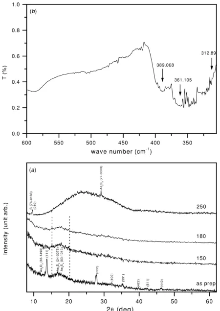
10 20 30 40 50 60
600 550 500 450 400 350
0.0 0.2 0.4 0.6 0.8 1.0
(a)
(440
)
(511
)
(422
)
(3
31)
(400)
(222)
(1
1
1
)
As
2
O3
(
3
6
-1490)
As
2
S3
(
24-0
075)
As
4
S4
(
83-1
013)
As
2
S3
(
2
7-0028
)
S
(
76-018
3)
(010)
as prep 250
180
150
In
tens
it
y
(
u
ni
t ar
b.
)
2θ (deg)
312.89
361.105 389.068
(b)
T (
%
)
wave num ber (cm-1)
Figure 1.(a) XRD patterns of arsenic sulfide films, identifying the As2O3component in the as-prepared film and assigning the observed
peaks for the samples heated; (b) FTIR spectra of the arsenic sulfide precipitate obtained from the chemical deposition bath.
energy applications [17]. The present work on chemically
deposited arsenic sulfide (As2S3) thin films has also been
motivated by the versatility offered by chemically deposited
bismuth sulfide [18,19], bismuth selenide [20] and antimony
selenide [21] with prospects for producing I–V–VI or III–V
compounds for photoconductive or photovoltaic applications. However, they would have a wide range of applications wherever large area coatings of these materials are required at a comparatively low cost on a choice of electrically conductive or non-conductive planar, porous or nanostructured substrates
or templates [22].
We report here that adherent and specularly reflective thin films of arsenic sulfide of thickness 300 nm can be deposited on glass substrates treated with organosilane, in a similar manner
as reported previously for depositing adherent Bi2S3 thins
films [23]. Structural, optical and electrical characteristics
will be presented. We report the formation of InAs through
heating an As2S3–In layer either in air or nitrogen, essentially
following the same methodology as reported by us in
producing InSb films [16]. We also noted that in a previous
work on amorphous As2S3 thin films, it was reported that
InAs is formed between As2S3and In contact [24]. We shall
present the optical and electrical characteristics of InAs films
formed with some amount of In2S3 or In2O3, depending on
whether the layer was heated in nitrogen or air. The procedure adopted here offers a relatively less expensive, large area
method for producing III–V/III–VI composite thin films for
distinct applications.
2. Experimental details
2.1. Chemical bath deposition of As2S3thin films
2.1.1. Substrates. The deposition was carried out on Corning
microscope glass slides (75 mm×25 mm×1 mm thickness)
in a solution of organosilane in a similar way as reported
in [23]. For this treatment, a solution of organosilane
was prepared by adding 2 ml of
N-[3-(trimethoxysilyl)-propyl]aniline, C12H21NO3Si (Aldrich) to a mixture of
90 ml of methanol and 10 ml of water. The resulting mixture
was heated at 50◦C for 30 min with stirring and afterwards
the glass slides were kept immersed in this hot solution for
1 h. The glass slides were then dried at 80◦C for 30 min
and utilized for the chemical deposition of films. The role of organosilane in building covalent bonds to glass surface which would thus serve as a coupling agent for a successive coating and the optimum conditions for substrate treatment have been
discussed earlier by many authors [25].
2.1.2. Solution of arsenic(III). A weighed quantity (1.9784 g)
of arsenic(III) oxide, As2O3 (Spectrum Chemicals, 99.5–
100.05 assay), was dissolved in a small quantity of water with an addition of 8 ml of concentrated HCl. Subsequently, the volume was made up to 100 ml in a volumetric flask by adding deionized water.
2.1.3. Deposition of the thin films. A deposition bath was prepared by adding with stirring 20 ml of 1 M
solution of sodium thiosulfate, Na2S2O3·5H2O (Baker
Analyzed Reagent), to 40 ml of the As(III) solution taken in a 100 ml beaker, and the volume was made up to 100 ml. The starting pH of this solution is 2. Glass slides treated in organosilane were placed in the bath with a slight inclination
against the wall of the beaker and maintained at 35◦C in a
circulation bath. The substrates were coated with films, which appear yellow in transmitted light and different tones of colour in reflection as the deposition proceeds. The typical duration of deposition was 6 h. The films were washed well with deionized water and dried. Specularly reflective thin films deposited on the side of glass slide that faced the wall of the beaker during the deposition were kept for analysis; the films on the other side were removed by scrubbing with cotton swabs moistened in HCl and subsequently with methanol to remove any organosilane residue.
Thickness measurements.Film thickness was measured using Alpha Step 100 (Tencor, CA). A slit was opened to serve as a step by scraping off the film from the substrate with a sharp splint. The thickness of the film deposited for 6 h in the bath was 300 nm. An estimate of the thin film yield was made using depositions on an array of substrates held together at a separation of 2 mm between each other. An acrylic lid with equidistant slots held the substrates vertically inside the bath. From the volume of the solution held between pairs of substrates and the thickness of the films, the thin film yield was estimated as 16%. This is the percentage of As in the
bath recovered as As2S3(or as a composite As2O3/As2S3; see
section 3) thin film, evaluated following the procedure reported
in [26]. The deposition technique may be improved further
to reduce the precipitation and hence improve the thin film
yield. Basically at small substrate separations,<1 mm, thin
film yield>50% may be achieved, though the maximum film
thickness would be typically<100 nm [27].
2.2. Vacuum evaporation of In
Glass substrates coated with arsenic sulfide thin films of thickness 300 nm were mounted on the substrate assembly,
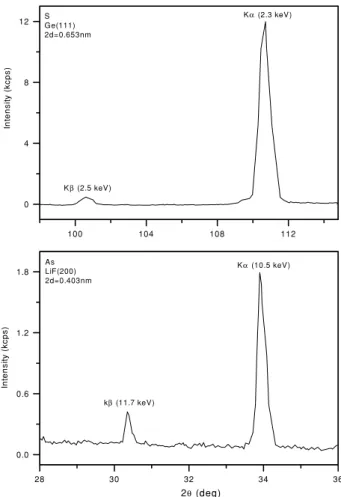
28 30 32 34 36
0.0 0.6 1.2 1.8
100 104 108 112
0 4 8 12
In
te
n
s
it
y
(
k
c
p
s
)
Kα (2.3 keV)
Kβ (2.5 keV) S
Ge(111) 2d=0.653nm
In
te
n
s
ity
(
k
c
p
s
)
2θ (deg)
Kα (10.5 keV)
kβ (11.7 keV) As
LiF(200) 2d=0.403nm
Figure 2.XRF spectra indicating the location of S and As peaks for
the as-deposited film of As2S3/As2O3, 300 nm in thickness.
14 cm above a molybdenum boat in a thermal evaporation unit. A weighed quantity (5, 16 or 50 mg) of 99.999% purity indium wire (Aldrich) was placed in the molybdenum boat.
After evacuating the chamber to a pressure of 10−6mbar, the
boat was heated to evaporate the indium completely. As the In film was soft, Alpha Step thickness measurement was not suitable. Film thickness was estimated using the deposition geometry, allowing for the directionality of the crucible:
≈15, 50 and 150 nm of In deposited on the As2S3film by
evaporating 5, 16 and 50 mg, respectively, of In.
Heat treatment of the films Samples of the films of arsenic sulfide deposited from the bath above were heated in air
and nitrogen at different temperatures: 150 to 250 ◦C for
30 min each. Heating in air was done in a Lindberg
furnace while that in nitrogen was done in a vacuum oven
of T-M vacuum products. For annealing in nitrogen, the
chamber was evacuated to 20 mTorr with the samples in, and subsequently nitrogen was introduced to increase the pressure up to 400 mTorr before raising the temperature of the furnace to the required value. The flow of nitrogen was maintained through the 30 min heating of the sample after attaining the temperature.
2.3. Characterization
X-ray diffraction (XRD) patterns of the films, for both
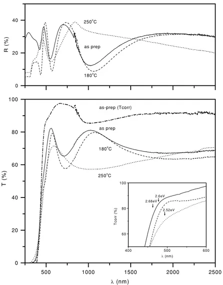
500 1000 1500 2000 2500 0
20 40 60 80 100 0 20 40
as-prep (Tcorr)
400 500 600
60 80 100
2.52eV 2.6eV 2.68eV
Tc
o
rr (%)
λ (nm )
180o
C as prep
250o
C
T (%)
λ (nm)
180o
C as prep 250o
C
R (%)
Figure 3.Optical transmittance (T) and specular reflectance (R) spectra of the as-deposited As2S3/As2O3film and As2S3film produced
through heating the same at 180 and 250◦C. TheTcorrcurves were obtained by correcting the transmittance curves for reflectance loss.
Rigaku D-Max 2000 diffractometer using Cu Kα radiation.
A Brucker Equinox 55 FTIR spectrophotometer was used for recording the spectra of the precipitate obtained from the chemical bath dispersed in a KBr pellet. X-ray fluorescence (XRF) spectral data of the as-prepared films were recorded on a Philips MagiX Pro x-ray fluorescence spectrometer with a tube voltage of 60 kV and a current of 60 mA, using
an LiF (2 0 0) analyser crystal (2d = 0.403 nm) for As
Kα line and a Ge crystal (2d = 0.653 nm) for S Kα line.
Optical transmittance and near-normal (5◦incidence) specular
reflectance spectra of the films were recorded on a Shimadzu UV 3100 PC spectrophotometer with the light beam incident on the film side, against air and a front-aluminized mirror, respectively, as references. The electrical properties of the films were measured on a computerized system consisting of a Keithley 619 electrometer and a Keithley 230 programmable voltage source. Coplanar electrodes of silver paint of 5 mm length at 5 mm separation printed on the surface of the films made the electrical contacts for measuring the dark currents and photocurrents with an applied bias of 10 or 100 V. For the samples in the measuring chamber, sufficient time was given for the current to become steady before recording the measurements: typically for the first 20 s in the dark, the next
20 s under illumination of approximately 1 kW m−2 by a
tungsten–halogen lamp, and the last 20 s after shutting off the illumination for observing the dark decay. In some cases, a linear four-point probe method was also used to measure the sheet resistance in the films.
3. Results and discussion
3.1. Arsenic sulfide thin films
In nature, arsenic sulfide is present as mineral realgar
(pararealgar, As4S4, PDF 83-1013, monoclinic), orange-red
in colour with a melting point of 307 ◦C, and as mineral
orpiment (As2S3, PDF 24-0075, monoclinic), lemon yellow
in colour with a melting point of 320 ◦C [28]. It is also
documented in this reference that As2S3 is the compound,
which is readily formed when an acidified solution of As2O3
(present case) reacts with a source of sulfide ions (thiosulfate in the present case). In the present case, the colour of the films and precipitates formed was lemon yellow in daylight.
As2S3is known to sublime easily, at temperatures below the
melting point, as observed for the films deposited by the
As4S4 may be formed by heating equal atomic amounts
of S and As at 500–600 ◦C and sudden cooling to room
temperatures. However, heating could cause changes in
the composition of the films; the quantum confinement in semiconductor films can greatly change the optical band gap and consequently the colour of the material, from orange to yellow. In this section, we present the results obtained on chemically deposited arsenic sulfide thin films; issues of structure and composition, and optical and electrical properties are addressed.
Structural properties. Figure1(a) shows the XRD pattern of arsenic sulfide thin films obtained from the bath, recorded at
grazing incidence withθ =0.5◦in a thin film mode. Clearly
identifiable peaks of As2O3(arsenolite, PDF 36-1490, cubic)
are seen in the pattern along with a broad peak near 2θ =
18◦. This broad peak may be assigned to reflections from
(1 1 1) planes of As4S4with intensity 100% at 2θ =17.318◦
and (2 0 0) planes with intensity 25% at 2θ =18.035◦in the
PDF standard 83-1013 or to that from (0 2 0) planes of As2S3
with intensity 100% at 2θ = 18.469◦ in the PDF standard
24-0075. When the films were heated at 150, 180 and
250 ◦C in air in order to enhance crystalline nature,
sublimation of the material led to reduction in the thickness of
the film: 300 nm (150◦C), 200 nm (180◦C), 170 nm (200◦C)
and 150 nm (250◦C). The XRD peaks of crystalline As2O3
disappear in these cases and the broad peak still persists.
This indicates the reaction of As2O3 with available sulfur
to form additional As2S3. Heating at 300 ◦C in air or in
nitrogen resulted in a total loss of the material from the
substrate. In the pattern recorded in the standard mode
for the film heated at 250 ◦C in air, the peaks appearing
at 2θ values around 9.6◦ and 29◦ match those from (0 1 0)
planes of sulfur reported in PDF standard 76-0183 and from (1 3 0) planes with 35% intensity reported for the mineral
orpiment in PDF standard 24-0075. We were not able to
establish the heat treatment conditions adequate to ascertain
the composition of the deposited films as As2S3through XRD
analyses.
Figure1(b) shows the infrared spectrum recorded in the
200–600 cm−1region, for the precipitate obtained from the
bath dispersed in the KBr pellet. Absorption bands due to
As–S stretching vibrations at 389, 361 and 312 cm−1may be
identified in this spectrum, based on an earlier reported work
[29] on the infrared and Raman spectra of realgar (As4S4) and
orpiment (As2S3). The S–As–S bending vibrations reported at
wave numbers<200 cm−1were not studied. If one considers
that the thin film has the same chemical composition as that of the precipitate obtained from the same bath, the available infrared data support the XRD results that the thin films formed are of arsenic sulfide.
X-ray fluorescence spectral data of the as-prepared films
are shown in figure 2. Using the LiF (200) analyser, the
As Kα(10.5 keV) fluorescence emission is detected along with
a weaker As Kβ(11.7 keV). With a Ge crystal (2d=0.653 nm),
S Kαfluorescence line (2.3 keV) is observed along with the
S Kβline (2.5 keV). Thus, the presence of As and S in the
as-deposited films is clearly established through the XRF results. However, we did not investigate the elemental composition in
the films to ascertain the composition as As2S3 through the
use of calibration curves with elemental mixtures. The optical
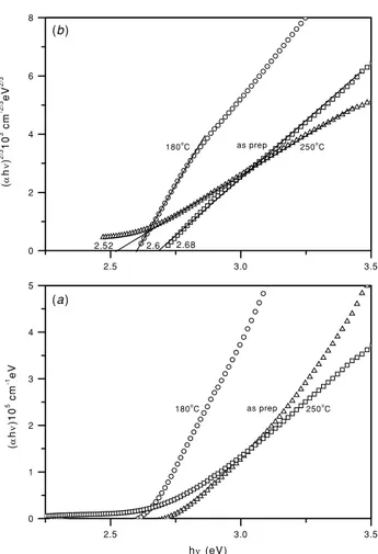
2.5 3.0 3.5
0 1 2 3 4 5
2.5 3.0 3.5
0 2 4 6 8
(a )
250o
C as prep 180o
C
(
α
h
ν
)1
0
5 cm -1eV
hν (eV)
(b )
2.68 2.6 2.52
180o
C as prep 250o
C
(
α
h
ν
)
2/
310 3 cm
-2
/3eV
2/
3
Figure 4.(a)(αhν)versushνplots for thin films of the as-deposited
As2S3/As2O3film and As2S3film produced through heating the
same at 180 and 250◦C; (b)(αhν)2/3versushνplots for the films.
characteristics of the films presented below helped to conclude
that the films have As2S3as a major component.
3.1.1. Optical and electrical properties. Figure3shows the
optical transmittance (T) and reflectance (R) spectra of the
films: as-prepared (300 nm in thickness), and after heating at
180 ◦C (200 nm approximately) and at 250 ◦C (150 nm) in
air for 30 min each. At near-infrared wavelengths of the
spectra, values of T + R or Tcorr = 100T /(100−R) are
approximately 90% (shown here for the as-prepared film), which testifies to the specularly reflective surface of the
films. In order to evaluate an optical absorption coefficient (α)
of the film as a function of the photon energy(hν), multiple
reflections at the air-film and film-substrate interfaces were
considered [30]:
α=
1
t
ln
(1−R)2+(1−R)4+(2RT )2
2T
. (1)
The plots of (αhν) versus hν for the films were evaluated
using the data in figure 3 and are shown in figure 4(a).
0 10 20 30
4.0x10⁻¹¹
4.5x10⁻¹¹
5.0x10⁻¹¹
0 20 40 60
4.0x10⁻¹¹
4.5x10⁻¹¹
5.0x10⁻¹¹
5.5x10⁻¹¹
photo
100 V
I (
A
)
t (s)
photo
100 V
I (A
)
Figure 5.Photocurrent responses in the As2S3film produced by
heating at 250◦C in a sulfur-rich atmosphere a chemically deposited film of As2S3/As2O3, 300 nm in thickness. The mode of
illumination is shown.
are allowed, but forbidden if the latter were derived from
d-states [31]. However, electronic transitions that are
forbidden by spectroscopic selection rules for individual electrons in individual atoms may take place with sufficient
probability in other situations, as discussed by Herzberg [32].
In the case of direct transitions (not involving phonons), which
are forbidden by conventional selection rules, a plot of(αhν)2/3
versushνwould have a straight line region, the intercept of
which on thehνaxis gives an estimate of a direct band gap. In
many cases where direct gaps have been reported, variation of the optical absorption coefficient with photon energy follows
a 3/2-law rather than a 1/2-law [31].
One can infer from the data in figure 4(a) that in
order to obtain a straight line plot, the variation of (αhν)
with hν should be rendered as: (αhν)2/3 versus hν (direct
gap, forbidden transition),(αhν)1/3versushν (indirect gap,
forbidden transitions) or (αhν)1/2 versus hν (indirect gap,
allowed transitions). In figure4(b),(αhν)2/3versushνplots
are given, which offered a straight line fit over the widest range of photon energies. The direct optical gaps obtained from these analyses for arsenic sulfide thin films are as follows: 2.68 eV
(as-prepared), 2.6 eV (heated in air at 180◦C) and 2.52 eV
(heated in air at 250◦C). The optical band gap of bulk As2S3
at 300 K is listed as 2.6 eV (direct) and for As4S4, 2.4 eV
[11]. The reported band gap values are in agreement with the
(1
1
0
) In
2
O3
5A 16A 50A
(c )
(1
0
9
) I
n2 S3
5N 16N 50N
(b)
In
tensi
ty
(
uni
t a
rb.
)
10 20 30 40 50 60 70
(311
)
(2
2
0
)
(1
11)
(a ) InAs (73-1984)
2θ (deg)
Figure 6.XRD patterns recorded using Cu Kαradiation on thin
films with the InAs component formed by heating in nitrogen (N) or air (A) at 250◦C, layers of As2S3/As2O3–In, with 5, 16 and 50 mg
of In used for evaporation. The standard PDF for InAs is given and assignation is made for the dominant peaks of additional crystalline phases.
observed colour of the minerals—yellow for As2S3(mineral,
orpiment) and orange for As4S4(mineral, realgar). The
as-prepared and heated films reported here are yellow; the optical band gaps of 2.5–2.65 eV obtained from the analysis of the
films (figure4(b)) are marked in the inset in figure3(a), on the
curves of optical transmittance corrected for reflectance loss. There is a good agreement between the values marked and the onset of strong optical absorption in the films. The observation that the valence band to conduction band excitation is best considered in terms of forbidden electronic transitions with a direct band gap is in agreement with the general behaviour of
many semiconductors [31].
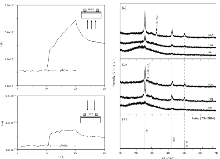
Figure 5 shows the photocurrent response under two
modes of illumination (as shown) of the films heated in
air at 250 ◦C in a sulfur-enriched atmosphere, measured
using a bias of 100 V. From the value of the dark current,
a dark conductivity of 10−8 −1 cm−1 is obtained for the
material. The photoconductivity of the films is low (also
≈10−8 −1 cm−1), but the increase in conductivity due to
illumination, from the 10th to 11th s or 20th to 21st s, is clearly observed in both modes of illumination. The electrical
conductivity reported for bulk As2S3 is extremely low,
10 20 30 40 50 60 70
(2
2
12)
(101
5)
(001
2)
(109)
In2S3 (25-0390)
2θ (deg) 50N
1.5
0.5 S
0.2
In
te
n
s
it
y
(a
rb
.
U
n
it
)
Figure 7.XRD patterns recorded for different angles of incidence
(θ=0.2, etc) of x-rays (Cu Kα) and in the standard mode (S) on the thin film with the InAs component formed by heating in nitrogen (50 N) at 250◦C a layer of As2S3/As2O3–In. The PDF for In2S3is
given to account for the minor phase; the major peaks correspond to InAs, as indexed in figure6.
it is usual that a relatively higher value of conductivity is observed for highly resistive materials such as this.
3.2. Formation of InAs by heating of As2S3/As2O3–In layers
InAs is a III–V compound semiconductor, which crystallizes in a zinc blende structure with a lattice constant 0.60584 nm, with a direct optical gap of 0.36 eV at 300 K and 0.42 eV when
extrapolated to 0 K [33]. A major application of this material is
in infrared detectors operating in a photovoltaic mode, which offer advantages over photoconductive detectors of PbSe or
PbS [34]. The formation of InAs from As2S3–In or mixed
As2S3/As2O3–In layers may be possible through reaction of
the type
As2S3+ 2In→2InAs + 3S↑.
Using the mass densities of As2S3 (3.4 g cm−3) or As2O3
(3.7 g cm−3), In (7.3 g cm−3) and InAs (5.8 g cm−3) and
the respective formula/atomic masses [35], one can determine
that 100 nm of As2S3 or As2O3 films would require about
40 nm or 60 nm, respectively, of In film for the reactions. The thickness of the InAs films resulting from the reaction would be 95 and 125 nm, respectively. In the present case
10 20 30 40 50 60 70
(3
00)
(214)
(1
1
6
)
(024)
(104
)
(0
1
2
)
(110
)
In
2O3 (22-0336)
2θ (deg) 50A
1.5
0.5 S
0.2
In
te
n
s
it
y
(a
rb
.
U
n
it
)
Figure 8.XRD patterns recorded using different angles of
incidence of x-rays (Cu Kα) and in the standard mode (S) on the thin film with the InAs component, formed by heating in air (50 A) at 250◦C a layer of As2S3/As2O3–In. The PDF for In2O3is given to
account for the minor phase; the major peaks correspond to InAs, as indexed in figure.6.
where the as-deposited films are of mixed composition, the
requirement of In for the reaction in As2S3/As2O3–In layers
may be considered as an intermediate to that of As2S3or As2O3
thin films. Thus, a complete reaction of As2S3/As2O3 of
300 nm in thickness would require a thickness of 150 nm of In; the InSb film produced would have a thickness of nearly
330 nm. In the deposition geometry utilized, we have
determined that the evaporation of 50 mg of In would suffice for a thickness of 150 nm. Smaller quantities of In—5 and
16 mg—as well were evaporated on As2S3/As2O3films to
study the evolution of the chemical reaction.
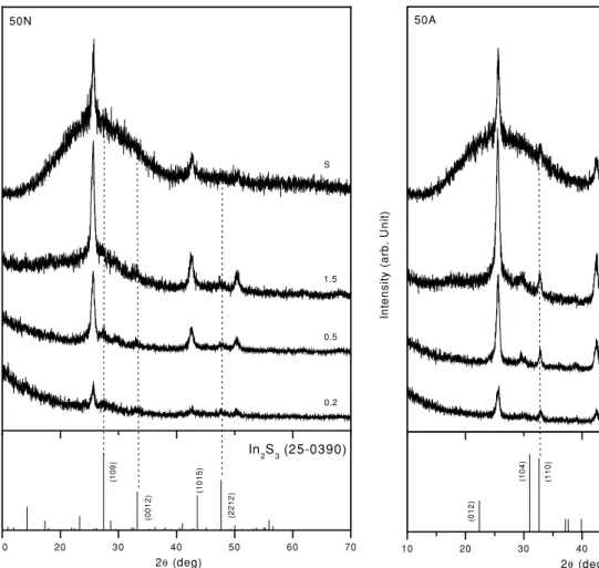
Structural evolution of the layer. Figure 6 gives the XRD patterns recorded in the grazing incidence mode with an angle
of incidence θ = 1.5◦ for the films resulting from heating
As2S3/As2O3–In films at 250◦C for 30 min. The labels 5 N,
5 A, etc denote the amount of In (in mg) evaporated to form a layer and the heating condition—N, nitrogen at
300 mTorr (figure 6(b)) and A, air at atmospheric pressure
(figure6(c)). The XRD pattern from PDF 73-1984 for InAs
is given in figure6(a) for comparison of the 2θpositions and
500 1000 1500 2000 2500 0
20 40 60 80 100 0 20 40
(a ) 16A Tcorr
16N Tcorr 0.81 eV
16A
16N 0.51 eV 0.67 eV
50A
T
, T
c
o
rr (%
)
λ (nm )
(b )
16N 50A
R (%)
Figure 9.Optical transmittance (T), reflectance (R) and corrected
transmittance (Tcorr) plots for thin films with the InAs component
formed by heating in air (16 A, 50 A) or nitrogen (16 N) at 250◦C layers of As2S3/As2O3–In with 16 or 50 mg of In used in
evaporation; the arrows indicate the optical band gap values obtained from figure10(c).
whether heated in nitrogen or air. In2S3may be present as a
minor component in the case of the layers heated in nitrogen; a
weak peak appearing at 2θof 27.46◦in figure6(b) may be due
to reflection from the (1 0 9) plane of tetragonal indium sulfide reported in PDF 25-039. For sample 50 A, a peak observed at
2θof 32.8◦is attributable to In2O3, as assigned in PDF 22-0336
for reflection from the (1 1 0) plane of rhombohedral (Hex)
In2O3. Peaks due to arsenic sulfide or arsenic oxide (figure1)
are absent in all the patterns.
Figures7and8show the XRD patterns recorded for the
films 50 N and 50 A, respectively, recorded at grazing angles
of 0.2◦, 0.5◦and 1.5◦as well as in the standardθ–2θ mode.
For the film 50 N, the relative intensity of the XRD peak
for the (1 0 9) plane of In2S3 with respect to that of the
(1 1 1) XRD peak of InAs is as follows: 0.2◦incidence, 0.3;
0.5◦incidence, 0.15; and 1.5◦incidence, 0.05. This confirms
that the In2S3layer is stratified near the top of a composite
InAs–In2S3layer. In the case of film 50 A, given in figure8,
the relative intensity of the XRD peak for the (1 1 0) plane
of In2O3with respect to that of the (2 2 0) XRD peak of
InAs is as follows: 0.2◦incidence, 0.3; 0.5◦incidence, 0.25;
and 1.5◦ incidence, 0.15. The variation here is less drastic.
Even in the recording of the XRD pattern in the standard
mode, the In2O3 peak is clearly noted. This suggests that
the film formed as a result of heating As2S3/As2O3–In in air
is a composite film, InAs/In2O3, in which the components
0.50 0.75 1.00 1.25
0.0 0.5 1.0
0.5 1.0 1.5 2.0 2.5 3.0 3.5
0 4 8 12
0.4 0.6 0.8 1.0 1.2
0.0 0.2 0.4
(b)
16A 16N 50A
(
α
h
ν
)1
0
5 cm -1eV
(a )
16A 50A
16N
(
α
h
ν
)1
0
5 cm -1 eV
hν (eV)
(c )
16A
0.81 0.51 0.67
16N 50A
(
α
h
ν
)
210 8 cm -2eV
2
Figure 10.(a)(αhν)versushνplots for thin films with the InAs
component formed by heating in air (16 A, 50 A) or nitrogen (16 N) at 250◦C layers of As2S3/As2O3–In with 16 or 50 mg of In used in
evaporation; (b) the same plot given for the near-infrared region of photon energies and (c)(αhν)2versushνplots for the films.
are rather uniformly distributed throughout the thickness of the film.
Optical and electrical properties. Figure 9(a) shows the optical transmittance and reflectance spectra of the films
16 N, 16 A and 50 A, plotted along with Tcorr curves;
figure9(b) shows the specular reflectance curves of the films.
It is obvious from the Tcorr plots that optical absorption
sets in at wavelengths in the 2000–2500 nm region for
these films, unlike in the case of As2S3/As2O3(as-prepared)
and As2S3 (heated) films shown in figure 3, in which the
optical absorption sets in at wavelengths <700 nm. The
optical transmittance of unheated As2S3/As2O3–In (16 and
50 mg) layers is <10% throughout the spectral region,
and the reflectance is >60%. Heating at 250 ◦C either
in air or nitrogen causes the indium layer to react with
As2S3/As2O3. Values ofTcorr→100% towards wavelength
2500 nm (and above) suggest the absence of a metal film in the layers after the reaction. This was concluded from
the XRD patterns discussed above. The arrows placed
on the Tcorr curves represent the optical band gap values
4.0x10⁻⁶ 6.0x10⁻⁶ 8.0x10⁻⁶ 1.6x10⁻⁵ 1.8x10⁻⁵ 2.0x10⁻⁵
-3.0x10⁻⁵ 0.0 3.0x10⁻⁵
-1.2x10⁻⁵ -6.0x10⁻⁶ 0.0 6.0x10⁻⁶ 1.2x10⁻⁵
-20 0 20
-4.0x10⁻⁹ 0.0 4.0x10⁻⁹
0 20 40 60
5.0x10⁻¹⁰ 1.0x10⁻⁹
16N
I(
A
)
50N
I(
A
)
dark 50N light 50N
I (
A
)
dark 16N light 16N
I (
A
)
dark 5N light 5N
I (
A
)
V (volts)
5N
I(
A
)
t (s)
Figure 11.Photocurrent responses under a bias of 10 V of thin films with the InAs component formed by heating in nitrogen at 250◦C
layers of As2S3/As2O3–In with 5, 16 and 50 mg of In used in evaporation. The right side plots are theI–Vcurves of the corresponding films.
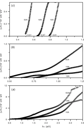
The plots of (αhν) versus hν evaluated from the
transmittance and reflectance spectra using equation (1) are
given in figure10(a). The optical absorption coefficient for
the films in the visible region (≈2 eV) is ≈105 cm−1 and
104 cm−1 in the near-infrared region (<0.7 eV), described
in figure10(b). The reported value of the optical band gap
for bulk crystalline InAs is 0.36 eV, and hence the analysis of optical band gap was done for this low energy region.
The plots of(αhν)2versushνin figure10(c) exhibit straight
line regions with intercepts of 0.51 eV for the sample 50 A, 0.67 eV for the sample 16 N and 0.81 eV for 16 A. The
reliability of these estimated values are seen in theTcorrplots
in figure 9(a)—the values approximately correspond to the
wavelength where the optical absorption sets in each case. The deviation of these band gap values from those reported for the bulk crystalline material is understood in terms of the quantum confinement effects in polycrystalline grains of
10–30 nm in the InAs component of the films, estimated from the XRD peak width analyses.
Figures 11 and 12 show the photocurrent response
measured at a bias of 10 V across pairs of electrodes 5 mm×
5 mm as well as theI–Vcharacteristics for V= −20 V to
+20 V, recorded in the dark and under illumination. The
following observations could be made.
(1) All the films are photosensitive; the silver print electrodes show ohmic behaviour over a larger range of bias voltage only in the case of thicker films. At the bias of 10 V used for the measurement of photocurrent response, a near-ohmic contact may be assumed.
(2) The presence of In2O3 phase in the films prepared by
0 20 40 60 1.2x10⁻¹²
1.4x10⁻¹²
1.6x10⁻¹²
7.0x10⁻⁹
1.4x10⁻⁸
2.1x10⁻⁸
2.8x10⁻⁸ 1.56x10⁻³ 1.60x10⁻³ 1.64x10⁻³
-3.0x10⁻³ 0.0 3.0x10⁻³
-2.0x10⁻⁸
0.0 2.0x10⁻⁸
-20 0 20
-8.0x10⁻¹²
-4.0x10⁻¹² 0.0 4.0x10⁻¹²
5A
I(
A
)
t (s)
16A
I(
A
)
50A
I(A
)
dark 50A light 50A
I(A
)
dark 16A light 16A
I(
A
)
dark 5A light 5A
I(
A
)
V (volts)
Figure 12.Photocurrent responses under a bias of 10 V of thin films with the InAs component formed by heating in air at 250◦C layers of
As2S3/As2O3–In with 5, 16 and 50 mg of In used in evaporation. The right side plots are theI–Vcurves of the corresponding films.
that In2O3:Sn (indium tin oxide, ITO) is a transparent
conductive coating with the high electrical conductivity of
103–104 −1 cm−1 [36] and that in sub-stoichiometric
(In2O3−x) material, the electrical conductivity can be
relatively high, 10−2–102−1cm−1. The latter aspect has
been discussed in the case of heated layers of CdSe–In [37]
and CdS–In [38]. The In2O3−xlayer with conductivity
≈400 −1 cm−1 was formed by heating the layers at
250◦C in air in those cases. Heating in nitrogen leads to
the formation of In2S3, as evidenced in the XRD analyses,
in which high conductivities as above have not been reported. Hence, InAs would dominate in the electrical conductivity of samples heated in nitrogen. From the
data presented in figures 11 and 12, the conductivity
of the InAs–In2O3 layer 50 A is ≈5 −1 cm−1 and
that of the InAs–In2S3 layer 50 N is two orders less,
≈0.05−1cm−1.
(3) The formation of InAs is favoured in comparison with
that of In2O3. In composite films formed in air involving
reduced quantities of indium (5 A, 16 A), the electrical current and hence the conductivity is less by about two orders of magnitude compared with those formed in
nitrogen. It was seen in the XRD patterns for these
samples that formation of InAs precedes that of In2O3;
XRD peaks of In2O3are not discernible for the samples
5 A and 16 A. While heating the films in air to produce InAs, oxygen is incorporated in grain boundaries, which increases the inter-grain potential barrier, impeding carrier transport. This would reduce the electrical conductivity, compared to InAs formed in nitrogen (5 N, 16 N).
In a 1968 paper, a carrier density of≈1024m−3and an
electron mobility of 0.3 m2V−1s−1were reported for InAs
at temperatures 300◦C or above [39]. Thus, the electrical
conductivity of such films is≈500−1cm−1. The electron
mobility for bulk crystalline InAs is 3.3 m2 V−1 s−1 [33],
and the carrier concentration (at 300 K) evaluated for intrinsic
material for a band gap of 0.36 eV is only 1021m−3, which
suggests that the electrical conductivity of intrinsic InAs is
≈5−1cm−1. However, a value 0.05−1cm−1for the sample
50 N obtained here may be accepted as a reliable value for the conductivity of InAs. This is because it has been established through theoretical models supported by experiments that charge carrier mobility and hence the electrical conductivity in polycrystalline materials may be less by one or more orders of magnitude due to chemisorbed oxygen in the grain boundaries
[40]. The presence of chemisorbed oxygen in the films
would bring down the dark current (conductivity) as well as photocurrent, but the photosensitivity, that is, the ratio of the
change in current to dark current would be higher [41]. In
some cases, the chemisorption of oxygen utilizes the photo-generated electrons, which would thus cause photocurrent to decrease with time, as seen in the case of sample 5 A in
figure 12. In samples where chemisorbed oxygen already
exists in the inter-grain region with the associated negative potential, photo-generated holes would neutralize the negative potential. This would lead to an increase in electron mobility and hence an increase in photocurrent during illumination, as observed for samples 16 A and 50 A, and in all cases of InAs
produced through heating in nitrogen (figure11).
4. Conclusions
We have reported here a method to deposit uniform specularly
reflective thin films of As2S3/As2O3with a possible presence
of sulfur, with an overall thickness of 300 nm. Heating the
films at temperatures above 150◦C converts the films to As2S3.
The films show an optical band gap of 2.64 eV (as-prepared) and 2.5–2.55 eV after heating. The films are very resistive;
electrical conductivity is≈10−8−1cm−1. With an In film
deposited by evaporation on the as-prepared film followed
by subsequent heating in air or nitrogen at 250 ◦C, InAs
forms as the dominant crystalline phase. The optical band gap of the material formed is 0.5–0.8 eV, depending upon the heating conditions. The electrical conductivity of the InAs film
formed this way is 0.05−1cm−1, low in comparison with
5−1cm−1for intrinsic InAs. For the InAs–In
2O3composite
film, a conductivity of≈5−1cm−1is observed, but this is
ascribed to In2O3, which is formed along with it. We have
found from XRD results and electrical measurements that
when an As2S3/As2O3–In layer is heated at 250◦C, either in air
or nitrogen, the readily occurring product is InAs. Formation
of the In2O3phase takes place in the layer heated in air or In2S3
when heated in nitrogen, only when In is present in excess.
Acknowledgments
We are grateful to Maria Luisa Ram´on Garcia for XRD measurements, Patricia Altuzar for XRF measurements
and Aaron Sanchez-Juarez for useful discussion. Jos´e
Campos helped with the electrical measurements and Oscar GomezDaza with optical measurements. Financial support for the project came from DGAPA-UNAM and CONACYT, Mexico.
References
[1] Cimpl Z, Kosek F and Lukes F 1987J. Non-Cryst.
Solids97, 98439
[2] Dikova J and Starboa K 2000Vacuum58490
[3] White K, Kumar B and Rai A K 1988Thin Solid
Films161139
[4] Santiago J J, Sano M, Hamman M and Chen N 1987Thin
Solid Films147275
[5] Yesugade N S, Lokhande C D and Bhosale C H 1995Thin
Solid Films263145
[6] Sartale S D and Lokhande C D 2000Mater. Res. Bull.351345
[7] Mane R S, Sankapal B R and Lokhande C D 2000Mater.
Chem. Phys.64215
[8] Rode A V, Zakery A, Samoc M, Charters R B, Gamaly E G and Luther-Davies B 2002Appl. Surf. Sci.197, 198481
[9] Sainov S and Stoycheva-Topalova R 2003Vacuum69365
[10] Smith J D 1973 Arsenic, antimony and bismuth
Comprehensive Inorganic Chemistry ed J C Bailar,
H J Emel´eus, R Nyholm and A F Trotman-Dickenson (Oxford: Pergamon) pp 547–621
[11] Madelung O 1992Semiconductors other than Group IV Elements and III–V Compounds, in Data in Science and
Technologyed R Poerschke (Berlin: Springer) pp 49–50
[12] Rodr´ıguez-Lazcano Y, Nair M T S and Nair P K 2005
J. Electrochem. Soc.152G635
[13] Rodr´ıguez-Lazcano Y, Nair M T S and Nair P K 2001J. Cryst.
Growth223399
[14] Nair M T S, Pe˜na Y, Campos J, Garc´ıa V M and Nair P K
1998J. Electrochem. Soc.1452113
[15] Bindu K, Campos J, Nair M T S, S´anchez A and Nair P K
2005Semicond. Sci. Technol.20496
[16] Nair M T S, Rodr´ıguez-Lazcano Y and Nair P K 2000J. Cryst.
Growth208248
[17] Nair P Ket al1998Sol. Energy Mater. Sol. Cells52313
[18] Nair M T S and Nair P K 1990Semicond. Sci. Technol.51225
[19] Nair P K, Huang L, Nair M T S, Hu H, Meyers E A and Zingaro R A 1997J. Mater. Res.12651
[20] Garcia V M, Nair M T S, Nair P K and Zingaro R A 1997
Semicond. Sci. Technol.12645
[21] Rodr´ıguez-Lazcano Y, Pe˜na Y, Nair M T S and Nair P K 2005
Thin Solid Films49377
[22] Niesen T P and De Guire M R 2001J. Electroceram.6169
[23] Huang L, Nair P K, Nair M T S, Zingaro R A and Meyers E A
1995Thin Solid Films26849
[24] Fitzgerald A G 1982Thin Solid Films98101
[25] Mittal K L (ed) 1992Silanes and Other Coupling Agents (Utrecht: VSP)
[26] Nair P K, Parmananda P and Nair M T S 1999J. Cryst.
Growth20668
[27] Nair P K, Garcia V M, GomezDaza O and Nair M T S 2001
Semicond. Sci. Technol.16855
[28] Greenwood N N and Earnshaw A 1984Chemistry of the
Elements(Oxford: Pergamon) p 674
[29] Forneris R 1969Am. Mineral.541062
[30] Schroder D K 1990Semiconductor Material and Device
Characterisation(New York: Wiley)
[31] Smith R A 1978Semiconductors(Cambridge: Cambridge University Press) p 313
[32] Herzberg G 1945Atomic Spectra and Atomic Structure(New York: Dover) p 154
[33] Sze S M 1981Physics of Semiconductor Devices(New York: Wiley) p 849
[35] Aylward G H and Findlay T J V 1974SI Chemical Data (Milton: Wiley)
[36] Frank G, Kauer E and K¨ostlin H 1981Thin Solid Films
77107
[37] Garcia V M, George P J, Nair M T S and Nair P K 1996
J. Electrochem. Soc.1432892
[38] George P J, Sanchez A, Nair P K and Huang L 1996J. Cryst.
Growth15853
[39] Howson R P 1968J. Phys. D: Appl. Phys.1939
[40] Orton J W, Goldsmith B J, Chapman J A and Powell M J 1982
J. Appl. Phys.531602