Development of III nitride based waveguides for application in all optical integrated circuits at 1 55 [my]m
226
0
0
Texto completo
(2)
(3) Universidad de Alcalá Escuela Politécnica Departamento de Electrónica. Development of III-nitride-based waveguides for application in all-optical integrated circuits at 1.55 µm Tesis Doctoral presentada por. Laura Monteagudo Lerma. Directores:. Dr. Miguel González Herráez Dr. Fernando B. Naranjo Vega. Alcalá de Henares, 2015.
(4)
(5) Abstract The development of new all-optical technology for data processing in future telecommunication networks has attracted a great interest since the last decade. This technology is aimed at the full exploitation of the large bandwidth of the optical fiber, avoiding the optical-electrical-optical conversion at each node of the traditional communication networks. This new all-optical technology requires different optical components which must be optically controlled. These devices are obtained by different semiconductor materials and are implemented in a miniaturized size within an all-optical integrated circuit operating at 1.55 µm, improving the reliability of the system while reducing costs. Since III-nitride materials have demonstrated a great potential for optical communication applications at 1.55 µm, the purpose of this work is the development of novel all-optical devices based on III-nitrides for their further integration in an ultrafast photonic integrated circuit operating at telecom wavelengths. Several all-optical waveguide devices based on different III-nitride structures on sapphire substrates and working at 1.55 µm have been developed during this Thesis. Firstly, different optical waveguides based on GaN/AlN quantum wells and quantum dots are optimized to act as saturable absorbers via their intersubband transitions. These waveguides could be used in all-optical switching processes. Secondly, the growth of AlN material by RF sputtering is optimized. The use of this material for fabricating passive optical waveguides is demonstrated. The linear optical behavior of the sputtered-AlN waveguides shows their suitability to act as low-cost passive interconnections within the all-optical integrated circuit. Finally, two sputtered-InN-based optical waveguides are optimized to operate as reverse saturable absorbers via two photon absorption processes. The obtained nonlinear.
(6) optical response of both waveguides opens the possibility of using them for all-optical limitation applications at telecom wavelengths..
(7) Resumen El desarrollo de una nueva tecnologı́a todo-óptica para el procesado de datos en las futuras redes de telecomunicación está generando un gran interés desde hace una década. Esta tecnologı́a está encaminada al total aprovechamiento del gran ancho de banda que proporciona la fibra óptica, evitando la conversión entre los dominios óptico y eléctrico necesario en cada nodo de las redes de comunicaciones actuales. Esta nueva tecnologı́a todo-óptica requiere de diferentes componentes ópticos que puedan ser controlados ópticamente. Estos dispositivos se obtienen a partir de distintos materiales semiconductores y se implementan de forma miniaturizada en un circuito todo-óptico integrado operando a 1.55 µm, mejorando de esta forma la fiabilidad del sistema y reduciendo su coste. Teniendo en cuenta que los nitruros del grupo III son materiales que han demostrado un gran potencial para aplicaciones en comunicaciones ópticas a 1.55 µm, el objetivo de este trabajo es el desarrollo de nuevos dispositivos todo-ópticos basados en éstos para su futura implementación en circuitos fotónicos integrados ultrarrápidos operando a longitudes de onda de telecomunicación. Durante esta Tesis se han desarrollado varios dispositivos de guı́a de onda basados en diferentes estructuras de nitruros del grupo III sobre substratos de zafiro y funcionando a 1.55 µm. En primer lugar, se han optimizado diferentes guı́as de onda ópticas basadas en pozos y puntos cuánticos de GaN/AlN para trabajar como absorbentes saturables a través de sus transiciones intersubbanda. Estas guı́as de onda podrı́an utilizarse en procesos de conmutación todo-óptica. En segundo lugar, se ha optimizado el crecimiento de AlN por sputtering de radiofrecuencia permitiendo su uso para la fabricación de guı́as de onda pasivas. El comportamiento óptico lineal de las guı́as de AlN por sputtering muestra su idoneidad para actuar como interconectores pasivos de bajo coste en un circuito todo-óptico integrado. Por último,.
(8) se han optimizado dos tipos de guı́as de onda basadas en InN por sputtering para funcionar como absorbentes saturables inversos mediante procesos de absorción de dos fotones. La respuesta óptica no lineal de ambas guı́as abre la posibilidad de utilizar estos dispositivos para aplicaciones en limitación todo-óptica a longitudes de onda de telecomunicación..
(9) Contents. 1 Introduction. 1. 1.1. Motivations . . . . . . . . . . . . . . . . . . . . . . . . . . . . . . . .. 1. 1.2. Objectives . . . . . . . . . . . . . . . . . . . . . . . . . . . . . . . . .. 6. 1.3. Outline of this Thesis . . . . . . . . . . . . . . . . . . . . . . . . . . .. 8. 2 Growth of III-nitrides 2.1. 11. Structural and morphological properties . . . . . . . . . . . . . . . .. 11. 2.1.1. Crystalline structure . . . . . . . . . . . . . . . . . . . . . . .. 11. 2.1.2. Polarization in wurzite nitrides . . . . . . . . . . . . . . . . .. 14. 2.2. Optical properties . . . . . . . . . . . . . . . . . . . . . . . . . . . . .. 19. 2.3. Film synthesis techniques . . . . . . . . . . . . . . . . . . . . . . . . .. 22. 2.3.1. Plasma assisted molecular beam epitaxy (PAMBE) . . . . . .. 22. 2.3.1.1. Plasma-Assisted MBE system used in this work . . .. 25. Sputtering . . . . . . . . . . . . . . . . . . . . . . . . . . . . .. 27. 2.3.2.1. RF magnetron sputtering system used in this work .. 33. Substrates . . . . . . . . . . . . . . . . . . . . . . . . . . . . .. 34. 2.3.2. 2.3.3. 3 Nitrides characterization techniques 3.1. 39. Structural and morphological characterization . . . . . . . . . . . . .. 40. 3.1.1. High-resolution x-ray diffraction (HRXRD) . . . . . . . . . . .. 40. 3.1.2. Atomic force microscopy (AFM) . . . . . . . . . . . . . . . . .. 46. i.
(10) 3.1.3 3.2. Field emission scanning electron microscopy (FESEM) . . . .. 47. Linear optical characterization . . . . . . . . . . . . . . . . . . . . . .. 48. 3.2.1. Visible/NIR transmittance measurements. . . . . . . . . . . .. 48. 3.2.2. Photoluminiscence (PL) measurements . . . . . . . . . . . . .. 50. 4 Optical waveguides: characterization 4.1. Beam propagation, fabrication and optical 53. Introduction to modal guiding in planar waveguides . . . . . . . . . .. 54. 4.1.1. Geometric optics: Ray approach . . . . . . . . . . . . . . . . .. 54. 4.1.2. Electromagnetic description: Wave equation. Matrix formalism. 58. 4.1.2.1. Wave equation . . . . . . . . . . . . . . . . . . . . .. 61. 4.1.2.2. Light polarizations: TE and TM cases . . . . . . . .. 65. 4.1.2.3. Guided modes. . . . . . . . . . . . . . . . . . . . . .. 70. 4.2. Optical waveguide types . . . . . . . . . . . . . . . . . . . . . . . . .. 71. 4.3. Numerical analysis: Finite-difference Beam Propagation Method . . .. 73. 4.4. Waveguide design and fabrication . . . . . . . . . . . . . . . . . . . .. 76. 4.4.1. Optical design . . . . . . . . . . . . . . . . . . . . . . . . . . .. 76. 4.4.2. Lithography . . . . . . . . . . . . . . . . . . . . . . . . . . . .. 77. 4.4.2.1. UV lithography or Photolithography . . . . . . . . .. 77. 4.4.2.2. e-beam lithography . . . . . . . . . . . . . . . . . . .. 79. Etching techniques . . . . . . . . . . . . . . . . . . . . . . . .. 80. 4.4.3.1. ICP-RIE . . . . . . . . . . . . . . . . . . . . . . . . .. 82. 4.4.3.2. Sputtering etching . . . . . . . . . . . . . . . . . . .. 83. Facet polishing . . . . . . . . . . . . . . . . . . . . . . . . . .. 83. Waveguide optical characterization . . . . . . . . . . . . . . . . . . .. 85. 4.5.1. Experimental setup . . . . . . . . . . . . . . . . . . . . . . . .. 85. 4.5.2. Optical characterization procedure . . . . . . . . . . . . . . .. 86. 4.4.3. 4.4.4 4.5. ii.
(11) 4.5.3. Propagation and coupling losses: Cut-back method . . . . . .. 88. 5 Nonlinear optical absorption saturation in GaN/AlN QW- and QD-based waveguides 91 5.1. Introduction . . . . . . . . . . . . . . . . . . . . . . . . . . . . . . . .. 92. 5.2. Optical and electrical design . . . . . . . . . . . . . . . . . . . . . . .. 96. 5.3. Structure growth and waveguide fabrication . . . . . . . . . . . . . . 102. 5.4. Linear and nonlinear optical measurements . . . . . . . . . . . . . . . 105. 5.5. 5.4.1. Theory of nonlinear optical absorption . . . . . . . . . . . . . 105. 5.4.2. Optical results at linear and nonlinear regimes . . . . . . . . . 109 5.4.2.1. Linear optical experiments: Cut-back method . . . . 110. 5.4.2.2. Nonlinear optical absorption saturation measurements 112. Conclusions . . . . . . . . . . . . . . . . . . . . . . . . . . . . . . . . 115. 6 Passive sputtered-AlN-based optical waveguides. 117. 6.1. Introduction . . . . . . . . . . . . . . . . . . . . . . . . . . . . . . . . 118. 6.2. AlN films synthesized by RF reactive sputtering . . . . . . . . . . . . 121. 6.3. 6.4. 6.2.1. Effect of RF power . . . . . . . . . . . . . . . . . . . . . . . . 122. 6.2.2. Effect of substrate temperature . . . . . . . . . . . . . . . . . 126. 6.2.3. Effect of substrate bias . . . . . . . . . . . . . . . . . . . . . . 127. 6.2.4. Two-step deposition method . . . . . . . . . . . . . . . . . . . 132. Sputtered-AlN-based optical waveguides . . . . . . . . . . . . . . . . 134 6.3.1. Waveguide optical design . . . . . . . . . . . . . . . . . . . . . 135. 6.3.2. AlN film deposition . . . . . . . . . . . . . . . . . . . . . . . . 137. 6.3.3. Waveguide fabrication . . . . . . . . . . . . . . . . . . . . . . 138. 6.3.4. Optical transmittance at 1.55 µm at linear and nonlinear regimes139. Conclusions . . . . . . . . . . . . . . . . . . . . . . . . . . . . . . . . 142. iii.
(12) 7 Nonlinear TPA process in sputtered-InN-based waveguides. 145. 7.1. Introduction . . . . . . . . . . . . . . . . . . . . . . . . . . . . . . . . 146. 7.2. InN deposition using AlN buffers by RF reactive sputtering . . . . . . 148 7.2.1. 7.3. 7.3.2. 7.5. 7.2.1.1. Structural characterization . . . . . . . . . . . . . . . 150. 7.2.1.2. Morphological analysis . . . . . . . . . . . . . . . . . 151. 7.2.1.3. Optical properties . . . . . . . . . . . . . . . . . . . 153. Sputtered-InN-based optical waveguides 7.3.1. 7.4. Structural, morphological and optical characterization . . . . . 149. . . . . . . . . . . . . . . . . 155. Waveguide optical design . . . . . . . . . . . . . . . . . . . . . 155 7.3.1.1. Columnar InN/AlN waveguide . . . . . . . . . . . . 156. 7.3.1.2. Compact InN waveguide . . . . . . . . . . . . . . . . 157. Waveguide fabrication . . . . . . . . . . . . . . . . . . . . . . 160. Linear and nonlinear optical characterization of sputtered-InN-based waveguides . . . . . . . . . . . . . . . . . . . . . . . . . . . . . . . . . 162 7.4.1. Linear optical experiments: Cut-back method . . . . . . . . . 165. 7.4.2. Nonlinear optical measurements . . . . . . . . . . . . . . . . . 166. Conclusions . . . . . . . . . . . . . . . . . . . . . . . . . . . . . . . . 169. 8 Conclusions and future work. 173. 8.1. Conclusions . . . . . . . . . . . . . . . . . . . . . . . . . . . . . . . . 173. 8.2. Future work . . . . . . . . . . . . . . . . . . . . . . . . . . . . . . . . 180. iv.
(13) List of Figures 1.1. 1.2. 2.1. 2.2. 2.3. 2.4. 2.5. 2.6. Evolution of the telecommunication networks from EICs based on Si-technology with transistors, resistors. . . to PICs consisting of different optical components such as lasers, detectors, switches, modulators. . . fabricated by diverse materials. . . . . . . . . . . . . .. 2. Direct band gap energies versus in-plane lattice constant for group-III-nitrides [Bau07]. . . . . . . . . . . . . . . . . . . . . . . . .. 5. Wurtzite structure of III-nitrides. Its primitive unit cell (dotted contour) is defined by the lattice vectors a~1 , a~2 and ~c. . . . . . . . . .. 12. (Left) Stacking sequence for wurtzite ABABA... planes along the h0001i axis. (Right) Staking sequence for cubic ABCABCA. . . planes along the h111i. . . . . . . . . . . . . . . . . . . . . . . . . . . . . . .. 13. Different polarities on wurtzite III-nitrides with the corresponding spontaneous polarization directions: (a) metal-polarity and (b) N-polarity. . . . . . . . . . . . . . . . . . . . . . . . . . . . . . . . . .. 15. Scheme of the spontaneous and piezoelectric polarizations and the induced electric field in a [0001]-wurzite metal-face GaN well pseudomorphically grown on AlN. . . . . . . . . . . . . . . . . . . . .. 19. Different atomic processes that can take place at the surface during MBE growth [Das12]. . . . . . . . . . . . . . . . . . . . . . . . . . . .. 23. Morphology of a growing film depending of the growth mode: Frank van der Merwe, Volmer-Weber and Stranski-Krastanow for various stages of the growth depending on the film thickness. . . . . . . . . .. 25. v.
(14) 2.7. Scheme of the PAMBE equipment used for the growth of the MBE samples analyzed in this Thesis. . . . . . . . . . . . . . . . . . . . . .. 26. (a) Schematic representation of the physical sputtering process. (b) Possible processes during material sputtering. . . . . . . . . . . . . .. 28. Scheme of the bombardment process in a sputtering system in planar diode configuration [Alb03]. . . . . . . . . . . . . . . . . . . . . . . .. 29. 2.10 Schematic diagram of the electrodes in a planar magnetron. . . . . .. 30. 2.11 Hysteresis process in reactive sputtering. . . . . . . . . . . . . . . . .. 32. 2.12 Schematic of the substrate biasing method used in this work for sputtering deposition. . . . . . . . . . . . . . . . . . . . . . . . . . . .. 33. 2.13 RF magnetron sputtering system used in this work together with the gas installation in the GRIFO facilities at the University of Alcalá. . .. 33. 2.14 (a) Illustration of the Si structure with (100) cubic plane and highlighted (111) hexagonal plane. The red-dashed triangle shows the relationship between silicon cubic and hexagonal phases. The hypotenuse corresponds to the lattice parameter of the hexagonal phase, aSi(111) , and the length of each side is half of the cubic phase lattice parameter, aSi(100) /2. (b) Scheme of the epitaxial relationship between III-nitrides and sapphire in (0001) plane. . . . . . . . . . . .. 35. 2.15 Experimental linear optical transmittance measurements of Si(111) and sapphire substrates in the visible/NIR range. . . . . . . . . . . . . . .. 37. 2.16 AFM images of the substrates used in this work: (a) sapphire and (b) AlN-on-sapphire template. . . . . . . . . . . . . . . . . . . . . . .. 38. 2.8. 2.9. 3.1. 3.2. Bragg’s reflection corresponding to two consecutive planes separated a distance d [Alb03]. . . . . . . . . . . . . . . . . . . . . . . . . . . . .. 41. Scheme of x-ray diffraction configurations: symmetrical and asymmetrical. The vector s is the scattering vector whose direction is given by the difference between the incident (k0 ) and diffracted (kz ) beams. . . . . . . . . . . . . . . . . . . . . . . . . . . . . . . . . . . .. 41. vi.
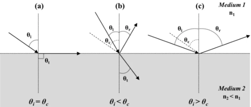
(15) 3.3. 3.4. Scheme of the rocking curve diffraction measurement. The materials grains responsible of the diffracted beam are highlighted in each case (blue color) [Nar03]. . . . . . . . . . . . . . . . . . . . . . . . . . . .. 42. Schematic representation of the 2θ/ω-scan. The diffracted planes responsible of the detected beam are highlighted in each case (blue color) [Nar03]. . . . . . . . . . . . . . . . . . . . . . . . . . . . . . . .. 43. 3.5. Example of a typical XRR scan of an AlN thin film pointing the critical angle (θc ) together with the estimation of the layer thickness in the inset. 44. 3.6. Scheme and real image of the diffractometer used during this work. .. 45. 3.7. Schematic representation of the AFM setup and FESEM image of the used tips. . . . . . . . . . . . . . . . . . . . . . . . . . . . . . . . . .. 46. Linear optical transmittance setup ranging from 350 nm to 1700 nm [VF11]. . . . . . . . . . . . . . . . . . . . . . . . . . . . . . . . . . . .. 49. 3.9. Schematic representation of the PL setup [Lah09]. . . . . . . . . . . .. 51. 4.1. Schemes of the behavior of an incident ray which travels from a certain medium (n1 ) to another with lower refractive index (n2 < n1 ) as a function of the angle of incidence: (a) θi = θc , (b) θi < θc and (c) θi > θc . 55. 4.2. Geometry of an asymmetric planar waveguide consisted of substrate (n2 ), guiding-layer (n1 ) and cover (n3 ). The refractive indices follow the relation: n1 > n2 > n3 . (Red) Relationship between the light wavevector and the propagation constant. . . . . . . . . . . . . . . .. 57. Scheme of the planar waveguide infinitely extended along the x - and z -direction. . . . . . . . . . . . . . . . . . . . . . . . . . . . . . . . .. 62. Schemes of the electric and magnetic fields in the case of TM- and TE-polarized light propagating along the positive direction of z -axis.. 65. 4.5. Schematic of several designs used for rectangular waveguides. . . . . .. 72. 4.6. Schematic of the transverse grid points and the propagation step in the finite difference method. . . . . . . . . . . . . . . . . . . . . . . . . .. 74. 3.8. 4.3. 4.4. vii.
(16) 4.7. (Left) Example of the transverse distribution of the real part of the refractive index at the input facet of a strip-loaded waveguide. (Right) Example of the contour map of the light mode amplitude at the output of the same waveguide. . . . . . . . . . . . . . . . . . . . . . . . . . .. 76. Scheme of the UV lithography process using negative photoresist under contact exposured. . . . . . . . . . . . . . . . . . . . . . . . . . . . .. 79. Procedure etching for the fabrication of ridge-type waveguides by using as the engraving protection layer (a) the developed photoresist and (b) the deposited metal. . . . . . . . . . . . . . . . . . . . . . . . . . . .. 81. 4.10 Different dry etching techniques depending on the working pressure and the excitation energy of the plasma together with the evolution of the figures of merit such as the etching anisotropy and the selectivity.. 82. 4.8. 4.9. 4.11 Polishing tools used in this work: (a) Apiezon wax piece and metal cylinders with (b) angled and (c) straight slots in which samples are fixed, together with the supporting pieces for the cylinders, (d) and (e). 84 4.12 Scheme of the experimental setup for optical characterization of the waveguides by monitoring the optical mode at the output of the structure. Inset: Scheme of a typical tapered lensed fiber (supplied by OZ Optics) used in this setup. . . . . . . . . . . . . . . . . . . . .. 86. 4.13 Scheme of the experimental setup for linear and nonlinear optical transmittance measurements of the waveguides. . . . . . . . . . . . .. 87. 4.14 Representation of the different scattering sources which likely produce propagation losses [Wu05]. . . . . . . . . . . . . . . . . . . . . . . . .. 88. 5.1. 5.2. (a) Scheme of the parabolic CB and VB in a semiconductor. Confinement geometric format and plot of the density of states, g(E), as a function of the excitation energy for (b) bulk material (0D), (c) QW nanostructure (1D) and (d) QD nanostructure (3D). . . . . . . .. 96. (a) Scheme of the energy levels for electron and holes in an ideal QW system along the confinement direction, z. (b) Cross-section of the E-k relation of a QW compared to that of the semiconductor bulk (dashed line). The energy levels in the CB are labeled as e1 and e2 , and h1 in the VB [VF11]. . . . . . . . . . . . . . . . . . . . . . . . . . . . . . .. 98. viii.
(17) 5.3. Scheme of the GaN/AlN waveguide format together with the dimensions susceptible to optimize. The active region can be based on QWs or QDs of GaN embedded in AlN barriers. . . . . . . . . . .. 99. 5.4. (a-c) Cross-section of the waveguide and normalized modal amplitude color maps at the output of GaN/AlN waveguides with different ridge widths: 2, 5 and 10 µm, respectively. . . . . . . . . . . . . . . . . . . 100. 5.5. Representative optical simulations which demonstrate the optimized ridge height for a 2-µm-wide waveguide leading to 350 nm. (Left) Normalized output modal amplitude profile with different ridge etching depths: 100, 200 and 350 nm. (Right) Estimated effective mode area as a function of the etching depth. . . . . . . . . . . . . . . . . . . . . 101. 5.6. (Left) Normalized output modal amplitude profile for both 5-µm- and 2-µm-wide waveguides with 350-nm-deep ridges. Black vertical lines indicate the location of the QD/QW regiones in the experimental structures. (Right) Conduction band profile of the active GaN/AlN superlattice considering the whole waveguide structure designed to obtain a resonant ISB transition at ∼ 1.55 µm. Dot-dashed line shows the depletion of the active structure when growing the QWs directly on the AlN template. Solid line illustrates the avoiding of the depletion of the QWs when introducing a minimum GaN buffer layer ∼25 nm. . 102. 5.7. HRTEM images of the active region of the samples containing 3 layers of (a) Si-doped GaN/AlN QWs and (b) Si-doped GaN/AlN QDs. . . 103. 5.8. Photolithography masks used for the definition of (left) the waveguide patterns and (right) the metallization patterns of the GaN/AlN-based waveguides. Orange regions correspond to the UV opaque chrome zones of the masks. . . . . . . . . . . . . . . . . . . . . . . . . . . . . 104. 5.9. FESEM images of a 2-µm-wide GaN/AlN waveguide (a) tilted 45◦ and (b) in plane view. . . . . . . . . . . . . . . . . . . . . . . . . . . . . . 105. 5.10 Scheme of the optical absorption saturation phenomenon in a two-electronic-level system at resonant energies (Egap ∼ hν). . . . . . 108 5.11 Near-field images taken with the IR camera of the obtained optical modes at the output of the (a) 5-µm-wide and (b) 2-µm-wide QD-based waveguides. . . . . . . . . . . . . . . . . . . . . . . . . . . . . . . . . 110. ix.
(18) 5.12 Cut-back method: Experimental TE-TM transmittance at minimum incident power (-12 dBm) as a function of the waveguide length for the devices under study (S1-S3). The experimental points correspond to the average of transmittance measurements in three waveguides for each waveguide length. . . . . . . . . . . . . . . . . . . . . . . . . . . 111 5.13 Transmittance for TE- and TM-polarized light (left) and transmittance increase for TM-polarized light (right) versus control pulse energy in (a,b) a 1-mm-long 5-µm-wide QW-based WG (S1), (c,d) a 1.5-mm-long 5-µm-wide QD-based WG (S2), and (e,f) a 1.5-mm-long 2-µm-wide QD-based WG (S3). . . . . . . . . . . . . . . . . . . . . . . . . . . . 114 6.1. (a) HRXRD 2θ/ω-scans and (b) ω-scans of AlN films deposited on c-sapphire substrates at 100% N2 , 0.47 Pa, 400 ◦ C and floating substrate as a function of the RF power. . . . . . . . . . . . . . . . . 123. 6.2. Growth rate for AlN films deposited on c-sapphire at a sputering pressure of 0.47 Pa, Tsubs = 400 ◦ C and pure nitrogen atmosphere as a function of the RF power applied to the Al target. . . . . . . . . 124. 6.3. (Left) rms surface roughness measured by AFM on 1×1 µm2 scanned area as a function of the RF power for the AlN layers under study. (Right) AFM images depending on the RF power: (a) 100 W, (b) 125 W, (c) 150 W and (d) 175 W. . . . . . . . . . . . . . . . . . . . . . . 125. 6.4. Linear fitting of the experimental square absorption coefficient of the optimized AlN layer deposited at 150 W presenting an estimated band gap energy of 6.02 eV. Inset: Linear optical transmittance spectrum of the AlN sample in the wavelength range from 190 nm to 2500 nm. . . 126. 6.5. FWHM of the rocking curve of the AlN(0002) x-ray reflection and grain size as a function of substrate temperature for AlN layers deposited at 150 W, 0.47 Pa and 100% N2 . . . . . . . . . . . . . . . . . . . . . . . 127. 6.6. (a) Real-time evolution of the current Ic during the AlN deposition process for 2 h for different values of substrate bias. (b) Saturation intensity, Is , as a function of the bias applied to the substrate during the AlN deposition process. . . . . . . . . . . . . . . . . . . . . . . . 128. x.
(19) 6.7. Estimated growth rate and film density by means of XRR measurements of the AlN samples deposited under different substrate bias. . . . . . . . . . . . . . . . . . . . . . . . . . . . . . . . . . . . . 129. 6.8. FWHM of the rocking curve of the AlN(0002) reflection and grain size as a function of the substrate bias. Best results of the FWHM and grain size for AlN deposited under unbiased conditions are 1.91◦ and 40.5 nm, respectively. . . . . . . . . . . . . . . . . . . . . . . . . . . . 130. 6.9. (a) HRXRD 2θ/ω-scans of AlN films deposited at Tsubs = 450 ◦ C and PRF = 150 W as a function of the substrate bias together with the unbiased AlN layer (F.S.). (b) HRXRD 2θ/ω-scan of the AlN sample consisting of a thin buffer layer (30 nm) biased at -15 V followed by a 240-nm-thick unbiased AlN layer (red line). This diffractogram is shown in comparison to the 120-nm-thick unbiased AlN film (black line).131. 6.10 (a) HRXRD 2θ/ω-scans of AlN films deposited under various substrate bias conditions: 120-nm-thick AlN at -15 V, two-step AlN with 15-nm and 30-nm-thick unbiased buffer layer followed by 120-nm-thick AlN at -15 V, and 120-nm-thick unbiased AlN. (b) HRXRD rocking curve around the AlN(0002) reflection peak for all the AlN films described in the previous caption. . . . . . . . . . . . . . . . . . . . . . . . . . . 133 6.11 AFM images of 120-nm-thick AlN deposited on c-sapphire (a) at floating substrate conditions; (b) at -15 V of substrate bias; and (c) at -15 V biased substrate conditions on top of 30-nm-thick unbiased AlN buffer layer (optimized two-step method). The rms surface roughness of the layers is 0.6, 0.7 and 0.4 nm, respectively. . . . . . . . . . . . . 134 6.12 (a),(c) Simulated waveguide cross-sections and normalized transverse modal amplitudes at the output facet for 2-µm- and 5-µm-wide waveguides, respectively. (b),(d) Normalized light amplitude color maps when propagating along the waveguide for 2-µm- and 5-µm-wide waveguides, respectively. . . . . . . . . . . . . . . . . . . . . . . . . . 136 6.13 (a) 45◦ -tilted FESEM and (b) 2×2 µm2 AFM images of the 570-nm-thick AlN layer deposited on sapphire for the development of the waveguides. The obtained rms is ∼1 nm. . . . . . . . . . . . . . . 137. xi.
(20) 6.14 Linear optical transmittance of the optimized AlN bulk material (black line) and theoretical calculations (red line) together with the dispersion relation for the ordinary refractive index estimated for this AlN layer.. 138. 6.15 (Left) Scheme of the photomask used in the UV lithography process for the patterning of the AlN waveguides. (Right) FESEM image of the cross-section and surface of the fabricated 2-µm-wide AlN waveguide.139 6.16 (a) Experimental optical transmittance of the 2-µm-wide and 1.8-mm-long AlN waveguides for TE- and TM-polarizations at linear and nonlinear regimes at 1.55 µm. (b) Cut-back method: Experimental relative optical transmittance between TE and TM polarizations at minimum incident optical power (-12 dBm) as a function of the waveguide lengths under study. . . . . . . . . . . . . . . . . . . . . . 140 6.17 Normalized amplitude at the output of the 2-µm-wide and 1.8-mm-long AlN waveguide exhibiting lower collected output light with the 8-µm-diameter-core optical fiber in the case of TE polarization compared to propagated TM light. . . . . . . . . . . . . . . . . . . . 141 7.1. Calculated apparent optical band gap as a function of the free carrier concentration by considering the Burstein-Moss effect and including the conduction band nonparabolicity [Wal04]. Typical limit values of the band gap for the sputtered InN films are also shown. . . . . . . . 146. 7.2. (a) HRXRD 2θ/ω-scan of sample S4 showing the (0001)-preferred growth orientation together with the AlN(0002) reflection corresponding to the thickest AlN buffer layer among the analyzed samples. (b) HRXRD rocking curves of the InN(0002) reflection peak of the InN layers (S1-S4). . . . . . . . . . . 150. 7.3. AFM images (2×2 µm2 scanned area) of the InN layers under study (S1-S4). . . . . . . . . . . . . . . . . . . . . . . . . . . . . . . . . . . 151. 7.4. FESEM images of all the InN films deposited on c-sapphire. . . . . . 152. 7.5. RT squared absorption coefficient (solid line) with a linear fit (dot-dashed line) as a function of the photon energy for the set of InN layers under study. . . . . . . . . . . . . . . . . . . . . . . . . . . 153. xii.
(21) 7.6. Normalized RT PL emission spectra depending on the excitation photon energy for the analyzed InN samples (S1-S4). . . . . . . . . . 154. 7.7. Optical simulations for the 2-µm-wide and 2-mm-long columnar InN waveguide: (Left) Effective area of the mode at the output of the single mode waveguide considering etching depths from 50 nm to 200 nm. (Right) Cross-section of the waveguide and normalized modal amplitude color maps at the output of the device considering 100 nm of etching depth. . . . . . . . . . . . . . . . . . . . . . . . . . . . . . 156. 7.8. (Left) AFM and (Right) FESEM images of the compact InN layer deposited directly on the sapphire substrate by RF reactive sputtering. 158. 7.9. Optical simulations for the 2-µm-wide and 2-mm-long compact InN waveguide: (Left) Normalized output modal amplitude profile for different etching depths from 50 nm to 350 nm. (Right) Plane view of the waveguide format together with the color maps of the normalized modal amplitude of light propagating along the 250-nm-deep waveguide confirming its multimode behavior. . . . . . . 158. 7.10 (Left) Cross-section of the waveguide and normalized modal amplitude color maps at the output of the deviced with the optimized etching depth of 350 nm. (Right) Normalized modal amplitude profile obtained at the output of the two optimized InN-based waveguides. Vertical solid lines indicate the thickness for the InN layer in each case. . . . . 159 7.11 Designed InN-based waveguides with the detailed dimensions: (Left) Columnar InN on double AlN buffer waveguide and (Right) Compact InN waveguide. . . . . . . . . . . . . . . . . . . . . . . . . . . . . . . 160 7.12 FESEM images of the fabricated columnar InN/AlN waveguides: (Left) surface view of the 2-µm-wide waveguide and (Right) cross-section and suface view of the 5-µm-wide waveguide. . . . . . . 161 7.13 FESEM images of the fabricated compact InN waveguides: (Left) surface view of the 5-µm-wide waveguide and (Right) cross-section of facet of the 2-µm-wide waveguide. . . . . . . . . . . . . . . . . . . . . 161. xiii.
(22) 7.14 Comparison of the linear optical transmittance of the original InN layer grown on sapphire, the single sapphire substrate and the InN layer after the Ar plasma etching. The agreement between the spectra of the etched InN and that of the sapphire substrate confirms the total etching of the original InN layer. . . . . . . . . . . . . . . . . . . . . . 162 7.15 Scheme of the TPA process in a two-electronic-level semiconductor. . 163 7.16 Cut-back method: Experimental TE-TM transmittance at low incident optical power (-2 dBm) as a function of the device length for (Left) the columnar InN/AlN waveguide and (Right) the compact InN waveguide. The experimental points correspond to the average of transmittance measurements in three similar waveguides for each length. . . . . . . 165 7.17 (Left) Transmittance and (Right) optical loss increase for TEand TM-polarized light versus the input pulse energy in (a,b) a 1.84-mm-long columnar InN-on-double-AlN waveguide and (c,d) a 2.07-mm-long compact InN waveguide. . . . . . . . . . . . . . . . . . 167. xiv.
(23) List of Tables 2.1. Lattice parameters at 300 K of bulk wurzite AlN, GaN and InN [Vur03] and deviation ratios from the ideal structure. . . . . . . . . . . . . . .. 12. 2.2. Spontaneous polarization for metal-face wurtzite III-nitrides [Vur03].. 15. 2.3. Values of the elastic coefficients [Vur03] and piezoelectric coefficients [Vur01] of AlN, GaN and InN. . . . . . . . . . . . . . . . . . . . . . .. 18. Commonly accepted values of the band gap energies at low and room temperature, Eg (0) and Eg (300 K), respectively, and Varshni constants α and β, of wurzite AlN, GaN and InN. . . . . . . . . . . . . . . . .. 20. Commonly accepted values of the ordinary and extraordinary refractive indices of AlN, GaN, InN and sapphire at 1.55 µm. Values with an asterisk have been estimated from our samples at 1.55 µm. The values used for the simulations of the optical structures and devices investigated in this work are underlined. . . . . . . . . . . . . . . . .. 22. Lattice mismatch between AlN, GaN and InN and Si(111) and sapphire substrates at 300 K. ∆aepi is the difference between lattice parameters of the layer and the substrate, obtained taking into account the epitaxial relationship explained in the text. The in-plane lattice parameters of Si(111) and sapphire are 3.840 Å and 4.758 Å, respectively [Fen08]. . . . . . . . . . . . . . . . . . . . . . . . . . . .. 36. 2.4. 2.5. 2.6. 5.1. Summary of the GaN/AlN-based waveguides under study concerning the implemented active nanostructures and ridge widths. . . . . . . . 110. 5.2. Summary of the experimental input pulse energy required for reaching 3-dB and 10-dB of optical transmittance contrast for TM light for the three samples under study. . . . . . . . . . . . . . . . . . . . . . . . . 112. xv.
(24) 6.1. Sputtering parameters investigated for the deposition of AlN films. . . 122. 7.1. Summary of the conditions for the four buffers under study: type of buffer, RF power applied to the substrate during the buffer layer deposition and buffer thickness. The sputtering pressure and substrate temperature are kept at 0.47 Pa and 450 ◦ C for all the material deposition in this study together with the nitrogen atmosphere. The optimized substrate bias for the biased-AlN buffer is -15 V. . . . . . . 149. 7.2. Summary of the structural and morphological properties of the analyzed InN films depending on the buffer used in terms of crystal quality, density of columns, columns size and rms surface surface. . . 151. 7.3. Summary of optical characterization results obtained using transmittance and PL measurements at RT for all the analyzed samples. . . . . . . . . . 154. 7.4. Results for the parameters related to the linear and nonlinear optical absorption for both sputtered-InN-based waveguides under study. . . 169. xvi.
(25) Chapter 1 Introduction This chapter presents a brief overview of the current technological limitations and challenges which arise in the future telecommunication networks. The main motivation in this field is focused on profiting the extremely large bandwidth that optical domain brings. In this work, different optical waveguide devices based on III-nitrides are developed with the aim of advancing in technology of future all-optical integrated circuits. This chapter also explains the three specific objectives of this study. The organization of the manuscript is introduced in the last part of the chapter.. 1.1. Motivations. Moving towards all-optical integrated circuits Electronic integration combines different electronic components on a chip forming the well-known electronic integrated circuit (EIC). Equally, photonic integration provides a possibility to combine active and passive optical components within the so-called photonic integrated circuit (PIC). While transistors, capacitors and resistors are typically integrated in EICs, these components are replaced in PICs by optical devices such as lasers, modulators, switches, multiplexers/demultiplexers, photodetectors, etc. Furthermore, like in electronics, a PIC provides cost, space, power and reliability advantages compared to the use of discrete single-function devices since connections are printed directly onto the chip. Thus, the development.
(26) 2. Introduction. of PICs allows to reach compact and cost-efficient structures which include a wide variety of optical functions for a broad range of applications, such as optical communications, sensing, biophotonics, spectroscopy, etc. During the last decades, the evolution from EICs to PICs arises as one of the most important future needs and challenges in the development of telecommunication networks. The beginnings of EICs came from J. Kilby when first integrated several transistors into a germanium-based single device in the late 60’s [Kil64]. Since then, the objective was to integrate more transistors and other electronic devices delivering exponentially greater data processing power while lowering the cost per device, improving reliability and reducing space and power requirements. Nevertheless, the wide functionality of EICs is not enough for covering the increasing bandwidth demand in telecommunication networks. The best solution would be the implementation of both types of devices integration, electronic and photonic, taking profit of their wide functionality. In fact, EICs provide many value-added functions in optical networks at a very low cost per device, such as switching, monitoring data transmission, system management and performance enhancement. The basis of telecom networks has significantly changed during the last decades, and nowadays the maximum bandwidth of the copper wire wants to be multiplied by 1000 through the use of PICs leading to ∼1 Tbps of data transmission rate per channel. In this sense, photonics is seen as the future of signal transfers because of the speeds that can be achieved.. Figure 1.1: Evolution of the telecommunication networks from EICs based on Si-technology with transistors, resistors. . . to PICs consisting of different optical components such as lasers, detectors, switches, modulators. . . fabricated by diverse materials..
(27) Motivations. 3. However, even considering the almost unlimited bandwidth provided by optical fibers, in current optical communication networks the limitation comes directly through the optical-to-electrical-to-optical (OEO) conversions. Despite the benefits in functionality and throughput that electronics can introduce within optical networks, the fact is that OEO conversion at each node is so expensive that its generalized use is not cost-effective. Thus, the tendency is moving towards the all-optical domain in telecom networks even taking into account that all-optical technologies are more expensive and complex than electronic Si-based technologies. Hence, in all-optical integrated circuits (ICs), electronic processing with the corresponding OEO conversion would be just relegated to the edges of the network while all the data transmission and switching processes would be performed in the optical domain. Because of these reasons, much effort has been put into the development of PICs, mainly addressing their use in all-optical communication at 1.55 µm. The PICs can be classified depending on their functionality (active or passive), their dimensions (large- or small-scale), the number of working wavelengths in use (singleor multi-channel) and the type of integration (hybrid or monolithic). The hybrid integration is based on multiple single-function optical devices assembled into a single package usually involving different materials and being possible to associate with EICs. At the same time, monolithic integration comprises many functions or devices into a single photonic material. This latter type of integration is the best solution in terms of simplicity and reliability since it includes optical components into a single device based on a single material. The capability of integrating as many different optical functions into a single material platform can be considered as the figure of merit of a PIC. Nowadays, optical components are fabricated by using different materials such as InP, GaAs, LiNbO3 , Si, SiO2 /Si, group-III-nitrides, etc. Among these different materials, most of them have not shown the capability of performing the most basic opto-electronic functions required in an optical transport network such as light generation, amplification, modulation and detection. Particularly, GaAs presents a limited working wavelength at ∼850 nm while LiNbO3 can not implement lasing and detection operations. On the other hand, although silicon is a low-cost material compatible with the CMOS-technology which presents high refractive index attractive for optical waveguiding, it also presents an indirect band gap which induces.
(28) 4. Introduction. a low light emission efficiency; besides, detection is not possible for wavelengths above ∼1.1 µm. Up to date, InP is the unique material platform which has been used for implementing large-scale monolithically integrated PICs. This material can provide both active and passive opto-electronic functions such as light generation, amplification, detection, wavelength multiplexing and demultiplexing, switching, etc. and integrate them in a single substrate leading in turn to costs reduction. Furthermore, the coupling losses between different-material packages or fiber-device couplings are completely avoided, thus, improving the reliability of the system. Concerning the industry’s production of these PICs, Infinera Corporation presented the first PIC achieving a capacity of 1 Tbps on a single photonic integrated chip. All the optical components were monolithically integrated onto an InP-based PIC operating with 10 channels at 100 Gbps of data rate per wavelength [Lal11]. Despite the benefits of the InP-platform, the drawback arises from its operation speed which is limited up to ∼500 Gbps per channel. The best way is to fabricate the PIC by using a single photonic material, but most of times it is not possible to provide many functions just with one material. In these cases, it is desirable to integrate different components by using materials from the same family, at least, taking profit of the better latticeand thermal-expansion-matching between them. A promising alternative is the implementation of a PIC based on III-nitrides. In fact, ambitious researches are currently being carried out focusing on all-optical signal processing technologies at 1.55 µm. Using this material family, further implementation of ultrafast all-optical ICs working at data transmission rates ≥1 Tbps per wavelength channel could be reached.. Why III-nitrides? Group-III-nitrides have emerged as attractive material constituents for photonic devices due to many reasons. First of all, the widespread direct band gap that III-nitride alloys can reach, ranging from the near infrared (NIR at ∼1.9 µm) for InN to the ultraviolet (UV at ∼200 nm) for AlN. This feature makes III-nitrides excellent semiconductors for efficient light emission within a wide spectral range thanks to the band gap engineering through alloys, heterojuntions and quantum-based.
(29) Motivations. 5. heterostructures. Figure 1.2 shows the direct band gap energy of wurtzite GaN, AlN and InN compounds and related ternary alloys (solid lines) as a function of the structural in-plane lattice parameter. It has to be pointed out that the tunable optical band gap gives advantage on the enhancement of nonlinear material properties when exciting at resonant energy.. Figure 1.2: Direct band gap energies versus in-plane lattice constant for group-III-nitrides [Bau07].. On the other hand, III-nitride semiconductors present electron mobilities about four times larger than silicon. Furthermore, the high bond energy between N and metal (Ga, Al, In) leads to materials with high thermal and chemical stability which are suitable for using in a wide variety of applications such as environmental applications, sensing and communication fields. In other respects, an important advantage of III-nitrides with respect to InP-based alloys is the better light coupling between silica optical fibers and III-nitride devices. This better coupling is due to the lower difference between refractive indices at 1.55 µm of III-nitrides (∼2-2.3) and optical fiber (∼1.46) than between InP (∼3) and fibers. Thus, the coupling losses due to Fresnel’s reflection are lower in the case of III-nitrides. Several optical components based on III-nitrides have been developed during the last two decades. The large conduction-band offset in the GaN/AlN quantum heterostructures (∼1.8 eV [Tch06]) may allow the fabrication of intersubband-based (ISB) emitters and detectors operating at 1.55 µm. In fact, several photodetectors have been developed based on quantum GaN/Al(Ga)N.
(30) 6. Introduction. heterostructures [Hof03][Var08]. On the contrary, up to date, it has not been reported any light emitter based on ISB transitions in III-nitrides working at 1.55 µm. On the other hand, 3-dB optical waveguide couplers at 1.55 µm have been developed based on GaN/AlGaN heterostructures [Hui03]. III-nitride semiconductors are definitely very promising materials for implementation in PICs aimed at all-optical communication applications at 1.55 µm since they cover the third window of telecommunications (1.53-1.57 µm) with different possibilities. The first one is based on the ultrafast intersubband transition (∼100 fs [VF08] in GaN/AlN quantum-based heterostructures while the second alternative approach comes from the interband transition of InN/InGaN heterostructures with relaxation lifetimes of a few ps [VF12a]. At the same, it is possible to operate at 1.55 µm through InN material whose optical bang gap is comprised within the C-band [Nar07]. In addition, the nonlinear two-photon-absorption (TPA) effect at 1.55 µm achieved in bulk InN by sputtering with subpicosecond recovery times [VF12b] can be also taken into account for active functions in optical communications. Furthermore, AlN and GaN are excellent candidates for passive optical waveguide devices at 1.55 µm since they are transparent within the visible/NIR range. It has to be noted that the implementation of these types of III-nitride waveguides on sapphire substrates would avoid the light absorption by the substrate due to its high transparency at telecommunications wavelengths. On the other hand, it has to be pointed out that III-nitrides can be deposited by sputtering taking profit of the low-cost solution it brings. In addition, this technique enables the regrowth of material at not harmful temperatures on previously deposited nitride-based devices, avoiding the likely damage due to high deposition temperatures by other techniques.. 1.2. Objectives. Taking into account the previous reasons, the main objective of this work is to investigate the optical response of different III-nitride-based waveguides performing.
(31) Objectives. 7. different functions for their implementation in further developed all-optical ICs. Thus, particularly, the objectives of this Thesis can be summarized in these three: To. design optical waveguides based on GaN/AlN QWs and QDs heterostructures grown by MBE. Once the waveguides are designed and fabricated, the main objective is to investigate their optical response at linear and nonlinear regimes focusing on the input pulse energy required to reach a 3-dB of transmittance increase of each structure via nonlinear saturable absorption at 1.55 µm. Special interest is given to the application of these devices in ultrafast all-optical switching functions.. To investigate the optical response of sputtered-AlN-based waveguides at low. and high input optical powers. For this purpose, optimization of the deposition conditions for the growth of AlN films by RF sputtering is firstly required together with the optical design and fabrication of the waveguides. The final aim is to demonstrate that these devices act as low-cost passive interconnecting pathways for being introduced in all-optical ICs at 1.55 µm. To analyze the nonlinear optical behavior of sputtered-InN waveguides. Within. this premise, efforts are firstly dedicated to the optimization of the deposition of InN films by RF sputtering. After that, optical simulations for performing the design of the waveguides and their fabrication are required. The aim is to obtain InN devices capable of acting as low-cost all-optical limiters operating at telecom wavelengths via the two-photon absorption phenomenon.. This work has been developed within the framework of several projects from different institutions: - CISTER (TEC2012-37958-C02-01) and FASTCOM (TEC2009-14423-C02-02), from Spanish Government calls. - FACTOTEM2 (S2009/ESP-1781) and SINFOTON (S2013/MIT-2790), from Comunidad de Madrid calls. - DIBOS (UAH2011/EXP-024) and DESLAP (CCG2013/EXP-052), from University of Alcalá calls..
(32) 8. 1.3. Introduction. Outline of this Thesis. This manuscript is divided in two main blocks. The first one includes Chaps. 2 to 4 and comprises the theoretical basis necessary for the comprehension of the study carried out in this Thesis. Particularly, the second chapter focuses on the material properties of wurzite III-nitride semiconductors (AlN, GaN, InN) in terms of structural, morphological and optical properties. The growth techniques used within the framework of this Thesis are also described there. Furthermore, Chap. 3 summarizes the different experimental techniques used along this work for the characterization of group-III-nitrides. The fourth chapter aims at being a basic guide on the theoretical concepts of integrated optics. A large section is dedicated to the analytic study of light modal guiding in planar waveguides as well as the numerical analysis technique used for investigating more complex non-planar optical devices. Furthermore, the theory of design and fabrication of optical waveguides is also treated while the description of the experimental setup used for optical characterization of the devices in the linear and nonlinear regimes is also described. On the other hand, the second block comprises Chaps. 5 to 7. They are focused on the experimental results obtained within this Thesis for the different optical waveguides under study, coinciding with the main three objectives expected in this work. Each chapter of this block describes the step-by-step process from the growth of the III-nitride materials and the design and fabrication of the waveguides until their optical characterization. Namely, Chap. 5 is dedicated to the investigation of the nonlinear optical absorption saturation presented in waveguides based on GaN/AlN QWs and QDs at 1.55 µm. These optical waveguides are intended to be promising active devices for implementing all-optical switching functions in III-nitride-based PICs. At the same time, Chap. 6 presents the growth and optimization of AlN films by RF reactive sputtering together with the design and fabrication of the AlN waveguide devices. The experimental results describe the capability of using these structures in III-nitride PICs as passive light pathways for interconnections between different devices. Likewise, the development of sputtered-InN-based optical waveguides is presented in Chap. 7. The nonlinear behavior of these InN-based structures at 1.55 µm is described via two-photon absorption processes demonstrating its usefulness as active all-optical power limiters in future III-nitride PICs..
(33) Outline of this Thesis. 9. Finally, Chap. 8 indicates the conclusions achieved along this study while providing new ideas for further improvement of the work presented in this manuscript..
(34) 10. Introduction.
(35) Chapter 2 Growth of III-nitrides This chapter presents a general overview of group-III nitride properties including a brief explanation of the two main thin film growth techniques which take part in this Thesis. Firstly, structural, morphological and optical properties are summarized for wurzite (Al, Ga, In)N compounds giving data about lattice parameters, elastic coefficients, polarization values, semiconductor band gap energies, refractive indices, etc. On the other hand, thin film deposition methods as molecular beam epitaxy (MBE) and sputtering are described. In addition, details of the growth equipment used during this work are also given.. 2.1 2.1.1. Structural and morphological properties Crystalline structure. (Al, Ga, In)N and their alloys crystallize in three different structures: hexagonal wurtzite (α-phase), cubic zinc-blende (β-phase) and rocksalt (γ-phase). While the wurtzite structure is the thermodynamically most stable at room temperature and atmospheric pressure, group-III nitrides can also be grown in the metastable zinc-blende structure and less commonly in the rocksalt one. The latter can be obtained only at very high pressures and cannot be stabilized by the epitaxial growth. This work only focuses on binary wurtzite-type nitrides..
(36) 12. Growth of III-nitrides. The wurtzite structure is determined by three main parameters: the edge length of the basal hexagon in the plane (0001) (in-plane lattice constant, a), the height of the hexagonal prism along the h0001i axis (out-of-plane lattice constant, c) and an internal parameter u defined as the metal-nitrogen bond length along the h0001i axis (see Fig. 2.1). In an ideal wurtzite crystal, the c/a and u/c ratios are 1.633 and 0.375, respectively. The real nitride structure presents a certain deviation from these expected values, which depends on the nature of the metal cation.. Figure 2.1: Wurtzite structure of III-nitrides. Its primitive unit cell (dotted contour) is defined by the lattice vectors a~1 , a~2 and ~c.. The lattice parameters of binary wurtzite AlN, GaN and InN at 300 K are indicated in Table 2.1.. Parameter. AlN. GaN. InN. a (Å). 3.112. 3.189. 3.545. c (Å). 4.982. 5.185. 5.703. c/a. 1.601. 1.626. 1.612. u/c. 0.380. 0.376. 0.377. Table 2.1: Lattice parameters at 300 K of bulk wurzite AlN, GaN and InN [Vur03] and deviation ratios from the ideal structure..
(37) Structural and morphological properties. 13. Figure 2.2: (Left) Stacking sequence for wurtzite ABABA... planes along the h0001i axis. (Right) Staking sequence for cubic ABCABCA. . . planes along the h111i.. For ternary compounds like Ax B1−x N, considering A and B as the metal elements and x as the concentration of metal A, the lattice parameters of a ternary alloy can be estimated using a linear interpolation of the lattice constants of the two forming binary alloys with respect to the concentration x (Vegard’s Law): aAx B1−x N (x) = xaAN + (1 − x)aBN. (2.1). cAx B1−x N (x) = xcAN + (1 − x)cBN. (2.2). The wurtzite structure shows hexagonal symmetry with the associated space group P63 mc(C46ν ). It consists of two hexagonal-close-packed (hcp) intertwined sublattices of metal (Ga, Al or In) and nitrogen (N) atoms, respectively, ideally shifted each other a ratio of 3/8c along the h0001i axis. By contrast, the zinc-blende structure presents a cubic symmetry with the associated space group F43m (T2d ) consisting of two interconnected face-centered cubic (fcc) metal-nitrogen sublattices and shifted each other a ratio 1/4 of the cubic diagonal (h111i) length. In both hexagonal and cubic phases, the atoms are tetrahedrically bonded. The major aspect which differentiates the wurtzite and cubic crystalline structures is the stacking sequence. The wurtzite phase stacks along the h0001i axis plane following an ABABA. . . sequence as illustrated in Fig. 2.2(left) and the cubic phase exhibits an ABCABCA. . . stacking sequence along the h111i axis shown in Fig. 2.2(right)..
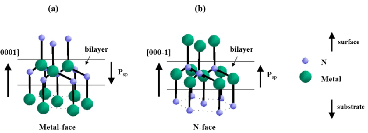
(38) 14. Growth of III-nitrides. In a hexagonal system, the three-index notation for crystallographic directions and planes has a equivalent one based on the Miller-Bravais indices. The Miller notation uses four indices, they being related to the projection of the considered direction on the vectors of the basic cell {a~1 ,a~2 ,a~3 ,~c} (see Fig. 2.1). Since a~3 =-(a~1 +a~2 ), a (hkl ) plane is equivalent to (hkil ) under Miller notation where i=-(h+k) and [hkil ] defines the direction perpendicular to the (hkil ) plane. This four-index notation takes into account that there are three equivalent symmetry axes a~1 , a~2 and a~3 in the plane perpendicular to the principal c-axis. Hence, the equivalency of, for example, planes such as (-1-120) and (2-1-10) is clearly shown in Fig. 2.1. The interplanar distance is given by the following equation: 1 d2hkl. 2.1.2. =. 4 h2 + k 2 + hk l2 + 2 3 a2 c. (2.3). Polarization in wurzite nitrides. The wurtzite structure does not present inversion symmetry along the c-axis leading to two different polarity configurations of these anisotropic uniaxial materials. A stretching out of the tetrahedrons is induced due to the difference in electronegativity between nitrogen and metal atoms which form the covalent bond. Since N presents higher electronegativity (∼3.0) than Al, Ga or In atoms (∼1.6-1.8), nitrogen atoms have higher tendency to attract the valence electrons from the metal atoms. Thus, an electrostatic dipole is induced in each tetrahedron. Then, due to the lack of symmetry along the c-axis of the wurtzite structure, the [0001] and [000-1] directions are not equivalent. The contribution of each tetrahedron to the total dipole leads to the generation of a macroscopic spontaneous polarization (Psp ). The terminology used for determining the different material polarities is: metal-polarity (Ga-, Al- and In-face) when growing along the [0001] direction leading to metal atoms at the end of the bilayer and nitrogen-polarity (N-face) when growing along the [000-1] direction finishing with nitrogen atoms at the bilayer. The sign of the polar axis is determined to be positive in the case of metal polarities and negative when dealing with nitrogen polarities. Figure 2.3 illustrates the difference between both types of polarity..
(39) 15. Structural and morphological properties. Figure 2.3: Different polarities on wurtzite III-nitrides with the corresponding spontaneous polarization directions: (a) metal-polarity and (b) N-polarity.. It must be pointed out that structures with different polarity are not at all equivalent showing large variations in physical and chemical properties. As an example, in the case of GaN, the N-face material presents a more reactive surface and worse crystalline quality compared to the Ga-face [Dim00][Mas05]. Since the spontaneous polarization vector points from the least to the most electronegative atom, i.e., from the metalto the N-atom, its value is negative for metal-face structures and positive for N-face crystals. Table 2.2 indicates the calculated spontaneous polarization for metal-face AlN, GaN and InN. AlN structure presents a larger value of the Psp compared to those calculated for GaN and InN. This difference is related to the large deviation of the AlN crystal from the ideal wurtzite structure (see c/a and u/c ratios in Table 2.1). Hence, the larger the deviation of the structure from the ideal wurtzite, the higher the value of the spontaneous polarization.. Psp (C/m2 ). AlN. GaN. InN. -0.090. -0.034. -0.042. Table 2.2: Spontaneous polarization for metal-face wurtzite III-nitrides [Vur03].. On the other hand, a piezoelectric polarization (Ppz ) can appear due to an induced distortion of the tetrahedrons when applying a mechanical stress. Nitride layers can not be obtained through homoepitaxial growth due to the lack of suitable.
(40) 16. Growth of III-nitrides. lattice-matched substrates with the same thermal expansion coefficients as nitrides. Thus, nitrides are mainly heteroepitaxially synthesized on substrates as sapphire, SiC or Si inducing strain within the layer during the growth. The piezoelectric polarization is related to the induced crystal strain, εij , through the piezoelectric tensor by: 0 0 0 e15 0 P~pz = 0 0 e15 0 0 e31 e31 e33 0 0. 0 0 × 0 . εxx εyy εzz εyz εzx. . (2.4). εxy where eij are the piezoelectric coefficients. Considering the symmetry in wurtzite crystals, there are only three independent piezoelectric constants: e15 , e31 and e33 . Since the material is usually grown along the [0001] direction on a substrate with different a lattice parameter, deformations along [0001] direction (εzz ) and in the plane perpendicular to h0001i axis (εxx , εyy ) are induced. These deformations or strains are defined by the following equations: c − c0 c0 a − a0 = εyy = a0. εzz = εxx. (2.5) (2.6). where c0 and a0 are the out-of-plane and the in-plane lattice parameters, respectively, of fully relaxed bulk material. Accordingly to Hooke’s Law, the stress σij is related to the strain εij through the tensor of the elastic module Cij . In the case of hexagonal crystal symmetry, five of the six elastic coefficients containing in the 6×6 matrix are independent as indicated by the following expression:.
(41) 17. Structural and morphological properties. . σxx σyy σzz σyz σzx. . . = . C11 C12 C13. 0. 0. 0. C12 C11 C13. 0. 0. 0. C13 C13 C33. 0. 0. 0. σxy. 0. 0. 0. C44. 0. 0. 0. 0. 0. 0. C44. 0. 0. 0. 0. 0. 0. C11 −C12 2. . . × . εxx εyy εzz εyz εzx. . (2.7). εxy. In this work, the crystal is grown along the [0001] direction. The in-plane stress is uniform (σxx =σyy ) and there is no stress along the c-axis (σzz =0). In this case, εyz =εzx =εxy =0 leading to a simplified diagonal deformation tensor referred by Eq. 2.8. Table 2.3 indicates the mechanical parameters of AlN, GaN and InN.. . . . . σxx σ yy 0. C11 C12 C13 = C 12 C11 C13 C13 C13 C33. . . εxx × ε yy εzz. . (2.8). Under these conditions, the in-plane and the out-of-plane deformation are related by: εzz = −. 2C13 εxx C33. (2.9). and, taking into account Eq. 2.4, the piezoelectric polarization in the (0001) plane X Y is nule, i.e., Ppz =Ppz =0, and the strain-induced piezoelectric polarization along the [0001] direction can be expressed as: Z Ppz =2. a − a0 C13 (e31 − e33 ) a0 C33. (2.10). Since [e31 -e33 C13 /C33 ]<0 for group III-nitrides assuming metal-face polarization (see Table 2.3), the piezoelectric field is positive (points to the [0001] direction) if the.
(42) 18. Growth of III-nitrides. material is under compressive strain (a<a0 ) or negative (oriented along the [000-1] direction) when the material is under a tensile strain (a>a0 ). Finally, in the case of a strained crystal, the total polarization (Ptot ) is the sum of both spontaneous and piezoelectric contributions and induces a total internal electric field within the material given by Etot = −. Ptot ε0 εr. (2.11). where ε0 is the vacuum permittivity and εr is the relative permittivity or dielectric constant of the material. AlN. GaN. InN. C11 (GPa). 396. 390. 223. C12 (GPa). 137. 145. 115. C13 (GPa). 108. 106. 92. C33 (GPa). 373. 398. 224. e31 (C/m2 ). -0.50. -0.35. -0.57. e33 (C/m2 ). 1.79. 1.27. 0.97. Table 2.3: Values of the elastic coefficients [Vur03] and piezoelectric coefficients [Vur01] of AlN, GaN and InN.. The growth of heterostructures along the polar [0001] direction leads to polarization discontinuities at the interfaces that induce polarization charge densities (σpol ), resulting thus in the generation of an internal electric field. For example, in quantum well (QW) heterostructures the charge density induced by the total polarization is equal to the difference of polarization between the barrier and the well: well barrier σpol = Ptot − Ptot. (2.12). Then, an internal electric field is induced within the well which is proportional to the charge density accumulated at the interface of the layers: Ewell =. −σpol ε0 εr. (2.13).
(43) Optical properties. 19. Figure 2.4: Scheme of the spontaneous and piezoelectric polarizations and the induced electric field in a [0001]-wurzite metal-face GaN well pseudomorphically grown on AlN.. Figure 2.4 shows the case of a metal-polarity GaN well pseudomorphically grown on a relaxed AlN barrier thus suffering a compressive strain. The directions and contributions of the spontaneous and piezoelectric polarizations, and the generated internal electric field are also indicated. This structure will be deeply studied in Chapter 5.. 2.2. Optical properties. Group III-nitride semiconductors present direct band gap which imply that the maximum of the valence band and the minimum of the conduction band are centered at the Brillouin zone. At this point, direct band-to-band absorption and emission processes can take place just involving photons with energies higher than the band gap. Ternary alloys allow to work within a wide spectral range. The band gap energy of the compounds can be tuned from the near infrared of the InN (∼0.64 eV, ∼1.9 µm) to the ultraviolet (∼6.2 eV, ∼200 nm) corresponding to the AlN, by changing the metal content..
(44) 20. Growth of III-nitrides. Eg (0) (eV) α (meV/K) β (K) Eg (300 K) (eV). Ref.. AlN. 6.25. 1.799. 1462. 6.14. [Vur03]. GaN. 3.51. 0.909. 830. 3.43. [Vur03]. InN. 0.69. 0.414. 454. 0.64. [Wu03]. Table 2.4: Commonly accepted values of the band gap energies at low and room temperature, Eg (0) and Eg (300 K), respectively, and Varshni constants α and β, of wurzite AlN, GaN and InN.. The band gap dependence on the alloy composition is modeled using a quadratic polynomial equation whose nonlinear coefficient is called the bowing parameter, b. This parameter takes into account the deviation from the linear interpolation given by the Vegard’s Law. Then, for a ternary nitride compound as Ax B1−x N, the band gap energy can be expressed as a function of the alloy composition as: Eg,Ax B1−x N (x) = xEg,AN + (1 − x)Eg,BN − b(1 − x)x. (2.14). The commonly accepted values of the band gap energy at low, Eg (0), and room temperature, Eg (300 K), are summarized in Table 2.4. In general, the temperature dependence of the band gap energy of semiconductors can be described by the Varshni’s Equation (Eq. 2.15). By fitting the experimental values of the Eg (T) to this equation, the optical parameters related to the band gap can be obtained. In this equation, Eg (0) is the band gap energy at 0 K, α is a constant and β is a parameter associated with the Debye temperature of the crystal [Var67].. Eg (T ) = Eg (0) −. αT 2 β+T. (2.15). Concerning the InN semiconductor, at the beginning, Tansley and Foley presented a value of the fundamental absorption edge for InN of 1.89 eV at room temperature which seemed to be well-established [Tan86]. This InN was grown by RF sputtering on glass substrates leading to polycrystalline films with residual carrier concentrations above ∼1019 cm−3 . Nevertheless, a controversy was raised when different groups suggested that the band gap energy values of InN grown mostly by MBE were in the.
(45) 21. Optical properties. range of 0.65-0.90 eV [Wu02][Mat02][Sai02]. Among them, Davydov et al. reported a band gap value of 0.9 eV for high quality InN films through different characterization techniques as optical absorption and PL spectroscopies [Dav02]. This value has converged to ∼0.64 eV [Wu03]. The difference between both ranges of band gap values for InN may be attributed to the crystalline quality of the InN films. InN grown by MBE and MOVPE presents high structural quality and low residual carrier concentration (∼1016 cm−3 ). Larger band gap energies in the range of ∼1.6-1.9 eV have been obtained for InN films deposited by sputtering usually presenting high doping levels in the order of ∼1020 -1021 cm−3 [Guo98][Sai01][VF12c]. This high free carrier concentration which induces the Burstein-Moss effect is one of the commonly accepted reasons of the InN large band gap together with the presence of oxygen and other dopant sources within the layers. As well as the band gap energy, the refractive index, n e(λ), and the absorption coefficient, α0 (λ), are crucial parameters for the application of these materials in optoelectronics and photonics. The refractive index is given by the following complex relationship: n e(λ) = n0 (λ) + iκ(λ). (2.16). where n e is the complex index of refraction, n0 (λ) is the real part of the refractive index which indicates the speed at which an electromagnetic wave propagates through the material while κ(λ) is the imaginary part called extinction coefficient which gives information about the amount of light which is absorbed when propagates through the material and its value is given by: κ(λ) =. α0 (λ)λ 4π. (2.17). Since the group III-nitrides in wurzite phase and sapphire are anisotropic uniaxial materials, they present two different refractive indices depending on the vibration direction of the light. They exhibit a certain refractive index when light vibrates parallel to the c-axis (extraordinary index, ne (λ)) and another when light vibrates perpendicular to the c-axis (ordinary refractive index, no (λ)) which is the same in all 360◦ ..
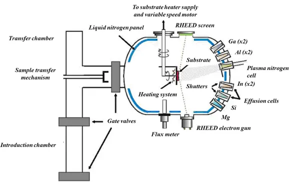
(46) 22. Growth of III-nitrides. AlN. GaN. InN [Web10]. Sapphire [Mal72]. n0. 2.120[Pas66] 2.042[Ozg01] 1.85*. 2.317[Bar73] 2.279[Ozg01]. 2.28*. 1.746 1.74*. ne. 2.160[Pas66] 2.089[Ozg01]. 2.305[Bar73] 2.315[Ozg01]. 2.09. 1.738. Table 2.5: Commonly accepted values of the ordinary and extraordinary refractive indices of AlN, GaN, InN and sapphire at 1.55 µm. Values with an asterisk have been estimated from our samples at 1.55 µm. The values used for the simulations of the optical structures and devices investigated in this work are underlined.. Table 2.5 summarizes the widely accepted values of the real part of the ordinary and extraordinary refractive index for AlN, GaN, InN and sapphire at the wavelength of interest for this study, 1.55 µm. Furthermore, values estimated from our samples are also included and highlighted with an asterisk.. 2.3. Film synthesis techniques. Thin film deposition techniques are mainly classified in four groups depending on the type of the involved process: evaporative processes as in plasma-assisted molecular beam epitaxy (PAMBE), glow-discharge as in sputtering, gas-phase chemical processes as in chemical vapor deposition (CVD) and liquid-phase chemical processes [Ses02]. The choice of the growth technique plays an important role in the properties of the obtained thin films. During the development of this Thesis, AlN and InN thin films have been deposited by sputtering and the quantum-confined heterostructures based on GaN/AlN have been grown by PAMBE. Thus, a general view of these two methods for the deposition of III-nitrides is given in this section.. 2.3.1. Plasma assisted molecular beam epitaxy (PAMBE). Epitaxial growth can be considered as the deposition of single crystal films which maintains a certain lattice alignment with respect to the single crystal substrate.
(47) Film synthesis techniques. 23. below. Particularly, heteroepitaxial growth is defined as the deposition of a material different from the substrate material. On the contrary, if both film and substrate materials are the same, the growth is considered homoepitaxial. PAMBE technique consists of the growth of a material under ultra-high vacuum through the interaction between evaporated atomic or molecular fluxes and the growing sample surface. The evaporated atoms impinge on a properly heated substrate where they condense and grow epitaxially. Group III-nitrides are provided by effusion cells and the gas flux is provided by a radio frequency (RF) N2 plasma cell.. Figure 2.5: Different atomic processes that can take place at the surface during MBE growth [Das12].. The main parameters to control the growth kinetics and thermodynamics are the material cells temperature, which determines the atomic fluxes limiting the arrival rate of atoms, and the substrate temperature, which controls the different processes that can occur at the substrate surface during the epitaxial growth. Figure 2.5 depicts the multiple surface processes that can take place during the epitaxial growth. Adsorption of the impinging fluxes can be occurred at the growing surface by chemical process (chemisorption through impinging atoms and surface atoms chemical bond sharing electrons) and by physical process (physisorption through Van der Waals forces). Difussion and desorption of species can be occurred due to the mobility of the atoms at a certain substrate temperature. These species will not be incorporated to the layer. Nevertheless, others will incorporate either by step-edge growth forming atomic terraces, or by cluster nucleation..
(48) 24. Growth of III-nitrides. PAMBE presents several advantages over other growth techniques as: - Growth under ultrahigh vacuum (10−11 mBar). - In-situ growth control by Reflection High-Energy Electron Diffraction (RHEED). - Good layer thickness control due to low growth rate (less than one monolayer per second) and excellent smooth surface morphology, thanks to the RHEED system. - Precise control of the beam fluxes. - Growth of complex heterostructures with many different layers and high abrupt interfaces. - Not very high growth temperature (700-750 ◦ C).. It has to be pointed out that the RHEED allows to real-time monitor the evolution of the growing material. In particular, the number of the monolayers grown, the change of its lattice parameter, its surface morphology and the likely transitions between different dimensional growth 2D-3D can be measured. The RHEED system is based on the collection of the electrons diffracted by the growing surface under ultrahigh vacuum by means of a fluorescent screen. Streaky diffraction patterns correspond to flat surfaces (∼2D) on the growing sample while rough surfaces (∼3D) present spotty diffraction patterns. PAMBE is widely used for the synthesis of nanometer-scaled structures based on different materials, like quantum wells (QWs), quantum dots (QDs) and nanowires (NWs). Depending on the substrate temperature and the relation between III-V elements, three different heteroepitaxial growth modes can be performed (see Fig. 2.6). The growth mode characterizes the nucleation and growth processes, and there is a direct correspondence between the growth mode and the film properties. The growth modes are the following: Frank van der Merwe growth [Fra49]: This growth is carried out layer by layer. resulting 2D structures. Atoms have enough mobility on the surface forming 2D.
Figure
![Figure 1.2: Direct band gap energies versus in-plane lattice constant for group-III-nitrides [Bau07].](https://thumb-us.123doks.com/thumbv2/123dok_es/7288359.348723/29.892.272.650.327.595/figure-direct-energies-versus-plane-lattice-constant-nitrides.webp)
![Figure 2.9: Scheme of the bombardment process in a sputtering system in planar diode configuration [Alb03].](https://thumb-us.123doks.com/thumbv2/123dok_es/7288359.348723/53.892.262.675.442.662/figure-scheme-bombardment-process-sputtering-planar-diode-configuration.webp)
+7
Documento similar
Finally, experiments with solar [17–34], atmospheric [35–45], reactor [46–50], and long-baseline accelerator [51–59] neutrinos indicate that neutrino flavor change through
Díaz Soto has raised the point about banning religious garb in the ―public space.‖ He states, ―for example, in most Spanish public Universities, there is a Catholic chapel
In the “big picture” perspective of the recent years that we have described in Brazil, Spain, Portugal and Puerto Rico there are some similarities and important differences,
No obstante, como esta enfermedad afecta a cada persona de manera diferente, no todas las opciones de cuidado y tratamiento pueden ser apropiadas para cada individuo.. La forma
The program is based on the following pillars: (a) students become the main agents of their learning by constructing their own knowledge; (b) the teacher must be the guide to
It is generally believed the recitation of the seven or the ten reciters of the first, second and third century of Islam are valid and the Muslims are allowed to adopt either of
ABSTRACT Transformation of the Specialized Knowledge of Future Primary Teachers on Fraction Division
From the phenomenology associated with contexts (C.1), for the statement of task T 1.1 , the future teachers use their knowledge of situations of the personal
In the preparation of this report, the Venice Commission has relied on the comments of its rapporteurs; its recently adopted Report on Respect for Democracy, Human Rights and the Rule
