Abstract— This paper illustrates the impact of including a flying capacitor in a Boost converter.
Both topologies, Boost and Boost with Flying Capacitor, are compared in terms of efficiency and volume. Results obtained from an optimization algorithm are validated through simulations and a hardware prototype.
Index Terms—DC-DC conversion, Boost, Multilevel, Flying Capacitor.
I. INTRODUCTION
n this paper, the Boost topology is compared with the Boost with Flying Capacitor topology, for that, a Matlab algorithm has been developed in order to calculate the losses and volume of the capacitors, transistors and inductor.
This two level topology requires two additional transistors (and their respectively drivers) and the flying capacitor. The multilevel topologies were first described in [1], in 1992, including a complete analysis of them. This idea was developed in order to allow high voltage conversion ratios using low voltage devices. Although the Boost with Flying Capacitor has two more transistors, the rated voltage is half of the Boost counterparts; therefore, the total silicon area should be similar for both converters in terms of voltage and current rating, but the inductor volume is reduced for the same switching frequency and current ripple as described in [2].
This document is divided in six sections. First, an introduction to the analyzed topologies is presented; Section II covers the operation principles. The methodology used to design the optimized converters is explained in Section III. In Section IV the prototype developed is presented. And finally, the conclusions and results are discussed in Section VI.
II. CIRCUITS AND OPERATION
This section explains the topologies operation and how to obtain Zero Voltage Switching (ZVS).
The switching sequence of the Boost with Flying Capacitor depends on the conversion ratio, VOUT/VIN. The specifications for the project are shown in Table I, as the conversion ratio is below 2, the switching sequence is presented for conversion ratios between 1 and 2.
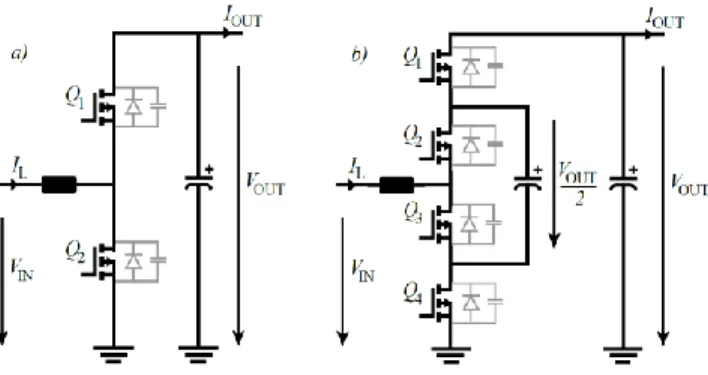
Both topologies are bidirectional because MOSFETs instead of diodes are used. The topologies are shown in Fig. 1. The flying capacitor is charged at half the output voltage, VOUT/2, and the capacitance is determined from the allowed voltage ripple, also, there is a minimum capacitance that can be selected to be able to switch above the resonant frequency of inductor and flying capacitor branch.
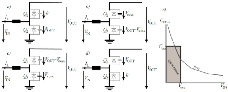
Both circuits are controlled to operate in Triangular Conduction Mode (TCM) to have negative current and be able to achieve ZVS, the drawback of the TCM is the high RMS inductor current. Fig. 2. shows the inductor current and MOSFETs state for both topologies.
Assuming that the flying capacitor voltage is half the output voltage the converter sequence is divided in 8 states:
Diego Serrano, Víctor Cordón, Miroslav Vasić, Pedro Alou, Jesús A. Oliver, José A. Cobos
Universidad Politécnica de Madrid, Centro de Electrónica Industrial
Impact of the Flying Capacitor on the Boost
converter
I
Fig. 1. Circuits including the parasitic diode and capacitor of the MOSFETs a) Boost b) Boost with Flying Capacitor.
TABLEI CONVERTER SPECIFICATIONS
Parameter Value
VIN 400 V
VOUT 750 V
POUT 2 kW
Vripple 2 %
ηmin 98 %
Volumemax 150 cm3
A. Charging the Inductor and Capacitor
First, Q2 and Q4 are turned on, the inductor is connected between the input and the flying capacitor, and hence, the inductor voltage is VIN-VOUT/2. Therefore, the inductor is being magnetized because VOUT/2 < VIN, and some energy is stored in the capacitor. This interval is used to control the output voltage.
B. ZVS in Q1
Q4 is opened with hard switching due to the high turn-off current, then, the inductor current simultaneously discharges the parasitic capacitance of Q1 and charges Coss of Q4. This interval should last until CossQ1 is fully discharged and CossQ4 fully charged. Assuming Coss ≪ Cfly, the equivalent capacitance seen from the inductor in this state can be approximated by CossQ1+CossQ4.
C. Discharging the Inductor
Q1 is turned on when the voltage across it is zero. Q2 was already closed and the inductor is placed between the input and the output as in the Boost converter. This interval must end with negative inductor current.
D. ZVS in Q3
The current through the inductor is negative. When the current is high enough to achieve ZVS Q2 is opened, the inductor current forces the parasitic capacitance of Q3 to discharge and CossQ2 to charge. At the end of this interval, the remaining current should be close to zero to avoid using higher peak to peak current than the minimum necessary. The equivalent capacitance seen from the inductor is CossQ2 + CossQ3.
E. Charging the Inductor and Discharging the Capacitor
Q3 is turned on with ZVS, the inductor is in series with the capacitor and the load, therefore the voltage in the inductor is VIN+VOUT/2-VOUT, the same as in A.
F. ZVS in Q2
It is similar to B, in order to achieve ZVS in Q2; Q3 is turned off without soft switching. The positive current in the inductor forces the current to flow through Q2 and Q3. G. Discharging the Inductor
Here Q2 is closed and A is repeated, magnetizing the inductor again.
H. ZVS in Q4
Finally, Q1 is closed, the negative current through the inductor discharges CossQ4 Once it is fully discharged, Q4 is open again and the A starts again.
All transistors turn on with ZVS but there are two hard turn-offs so switching losses due to this effect are high.
Regarding the current necessary to achieve ZVS further understanding of the switching transition is needed due to the nonlinear parasitic capacitance.
A complete explanation of nonlinear capacitance of the MOSFETs and the ZVS is done in [3]. A typical characteristic and a simplified model used are shown in Fig 3. The parasitic capacitance is modeled assuming that the capacitance is constant, Coss, below a given voltage, Voss, and negligible above this voltage value.
To explain how to obtain ZVS with the TCM operation the period when the current is negative will be described in detail, and just for the Boost converter for simplicity. First, the high side transistor, Q1, is closed; the inductor current is decreasing because the inductor voltage is negative. When the current flows from the output to the input and it is negative enough Q1 is opened and the current starts to charge CossQ1 but the voltage in the parasitic capacitance is still very low, at this point the high side parasitic capacitance is orders of magnitude higher than the low side capacitance due to the voltage dependence, and the current keeps falling. At the end of this period the current reaches its lowest value, then the low side parasitic capacitor has the lower voltage value, therefore, the capacitance increases, becoming the low side CossQ2 the dominant one, once it is discharged, the ZVS turn on can take place.
An easy analysis leads to the correct value of bottom current, if the input voltage is much higher than Voss, then the minimum current needed for ZVS can be approximated by:
L
V
V
C
I
2
·
oss·
in·
ossmin
(1)Same calculation can be done for the Boost with Flying Capacitor converter. The results are the same, just replacing Vin with the voltage used for magnetizing the inductor, in this case Vin-Vout/2.
Once the minimum current is known, the frequency in the Boost converter in TCM can be estimated as:
out in
out in in
in
V
V
V
V
L
V
I
I
f
·
2
·
·
2
·
1
min
(2)
If the inductance and parasitic capacitance is known the current waveform can be easily calculated. Similar reasoning can be done for the Boost with Flying Capacitor.
For low bandwidth control modes, capacitor voltage does not need to be measured. Assuming that the voltage in the capacitor is above VOUT/2 by a small amount, then, the slope of A will slightly decrease and E slope will slightly increase as well. If the duration of A and E are the same, the average current though the capacitor at the end of the period will be negative, therefore, the capacitor voltage will decrease. This operation leads the capacitor to the correct voltage without any control.
III. OPTIMIZATION METHODOLOGY
The optimization process developed in order to find the best combination of inductor capacitors and MOSFETs is covered in this section.
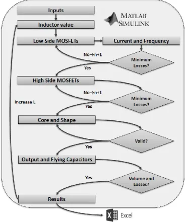
A Matlab algorithm has been developed in order to calculate the losses and volume of different designs for each topology. The objective of this algorithm is to calculate a list of designs for a given topology and component technology. A simplified flowchart of the algorithm done for the Boost with Flying Capacitor is shown in Fig 4. The process follows this scheme: A. Main loop
The optimization algorithm makes a sweep of inductances values, increasing the value every time.
B. Transistors loop
With the inductance value, a first loop finds the minimum number of low side MOSFETs.
With a first transistor number, the value for the current is calculated, including the negative current in order to have ZVS. Therefore, the frequency is established and the switching losses can be obtained. If the calculated temperature of the MOSFETs is over the limit, the process repeats the calculations with an additional transistor in parallel.
The losses in the MOSFETs includes the conduction losses, including the RON temperature effect but not the dependence with ID, the turn-off losses and the driving losses, there is no need for turn on losses calculation due to the ZVS.
Other loop is done from this MOSFETs number until it finds the number of MOSFETs that minimizes the losses: increasing the number of MOSFETs in parallel decreases the on resistance but increases the parasitic capacitance, therefore not only the switching losses increases but also the current needed to achieve ZVS and so the effective value of the current. The final designs include the result with minimum number of MOSFETs and the result with the optimum value because the optimum value is not always the best due to the volume increase.
Once the low side transistors number is obtained, a similar process is done for the high side MOSFETs, in this step the frequency and current are already known, and it is not necessary to change them because the current when the high side MOSFETs turns on is high enough and the effect of the ZVS in the current can be neglected. At the end of this step, all the losses and volume of the semiconductors are known. C. Inductor design
The next step in the process is to obtain an appropriate inductor; although this is not very accurate because some assumptions must be done.
A list of cores and materials is given to the program. For each combination the process checks if the inductor is suitable for the current waveform and inductance value.
The first step in the inductor design is to set the minimum number of turns, which is related to the inductor peak current and therefore to the maximum magnetic field; this maximum value is set to 0.7 of the saturation value.
The maximum number of turns is limited by a maximum gap length allowable, set as the 20 % of the total height of the core including both sections; this is done to reduce the mismatch due to the gap effect.
Then the number of turns is iterated. Instead of finding the optimum number of turns, all valid design are included in the results because not all the optimum inductor designs can be manufactured.
To calculate the inductor losses the wire section must be obtained; for the sake of simplicity neither wires in parallel nor Litz wire are included. A simple way to estimate the wire section is to set the percentage of winding area that is fulfilled with wire, in this application the value was 20 % because it gives results close to the obtained with PExprt, a tool for magnetic component design.
With the total wire area and the number of turns, the wire section is calculated. The DC losses are easily calculated.
It’s very difficult to include the proximity or gap effects, but the skin effect can be calculated, although some approximations are also done here.
The first harmonic frequency of the current is known, therefore the skin deep can be calculated, and, assuming that all the harmonic content is at the fundamental frequency the AC losses can be estimated.
Finally, the core losses are obtained with the Steinmetz equations, however those results are not very reliable because Steinmetz equations are defined only for a certain frequency range and the process uses the equations at any frequency.
The core temperature is obtained with the equations found in [4] for E cores. If the core temperature is above 100ºC the design is rejected. At the end of this step the inductor volume, assumed as the core volume, and the inductor losses are estimated.
However, important effects are not included so we expect the losses to be higher in real designs, but those losses are expected to be higher in the same way for both topologies, so the comparison remains fair although the results may change. D. Capacitor selection
The last step of the optimization process is to obtain the different capacitors.
The specifications of the capacitors are included in the process. With the maximum ripple allowed the minimum number of capacitors in parallel is obtained, also, for the minimum flying capacitor, the minimum resonant frequency is included.
The designs include the results with the minimum capacitance and also the results increasing one by one the number of parallel capacitors because there is no way to optimize the volume and losses here, therefore designs with more capacitor volume but less losses must be included.
To use low voltage devices, the output capacitor is spitted in two capacitors, the input capacitor and other capacitor is series placed between the input and the output.
The capacitor losses can be estimated through the ESR; however, this value is very dependent on the voltage, frequency and temperature condition so it is not very accurate. E. Components
In order to make this comparison fair, it is important to select MOSFETs with the same technology.
The Boost transistors must block the output voltage; therefore, Infineon IPW90R120C3 CoolMOS with 900 V breakdown voltage were used.
In the case of the Boost with Flying Capacitor, the maximum voltage across the MOSFETs is half the output voltage, Infineon IPB65R045C7 was selected, although they can block 650 V they present better FOM than the Infineon devices for 500 V.
The inductor design only includes E cores. Three different materials have been used so far: 3C94, 3C95 and 3F3.
For all the capacitors, TDK CeraLink 20 μF, 500 V was chosen. Nevertheless, it is very easy to include new components, or even use multiple components, if it is required. F. Results
At the end of the process the most important volume and losses contributions are estimated (the driver, sensors and control volume and losses are not included in this process). If the volume and losses are below the limit of the specifications the result is included in an excel file.
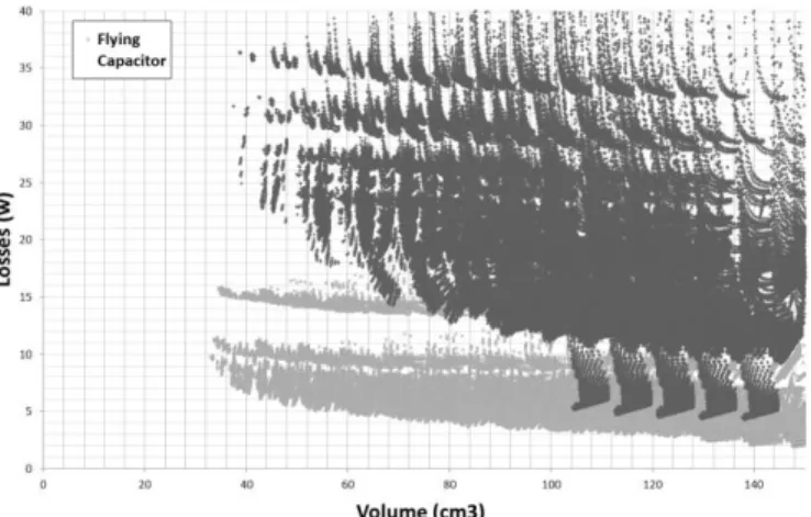
The obtained designs can be plotted as a function of the total volume and total losses and are shown in Fig 5. it clearly shows that the Boost with Flying Capacitor has better performance than the Boost, but it is important to note that those results are preliminary because the driver, measuring circuits and controller volume and their associated losses are not included, and the ZVS current estimation and inductor designs needs further improvements.
Simulations with “Gecko Circuits” simulator and “PExprt” software have been used to validate the topologies operation and the inductor design.
Fig. 5. Volume and losses of each design. The darker dots correspond to the Boost designs.
TABLEII
PROTOTYPE RESULTS:THEORETICAL AND MEASURED Theoretical Results
Core and Material E42/21/15 – N27
Number of turns and wire diameter 11 – 1.5 mm - 3 in parallel
Inductance 45.6 μH * 45.6 μH
MOSFETs Infineon IPB65R045C7
High Side MOSFETs 4 - 2 in parallel
Low Side MOSFETs 4 - 2 in parallel
Capacitors (in, out, fly) TDK CeraLink 20 μF, 500 V
Minimum current -4.33 A * -4.335 A
Switching frequency 27.4 kHz 32.64 kHz
Input voltage 400 V 401.65
Output voltage 750 V 750.03
Input power 2000 W 1988.17
Output power 1984.72 W 1968.82
Efficiency 99.24 % 99.02 %
Inductor losses 6.85 W
Capacitor losses 2.82 W
MOSFETs losses 5.60 W
Zero cross detector losses 0.27 W
Inductor temperature 79.10 C ≈ 71 C
Total Volume 57.89 cm3
IV. PROTOTYPE
A Boost with Flying Capacitor has been developed in order to verify the operation principles and the theoretical results.
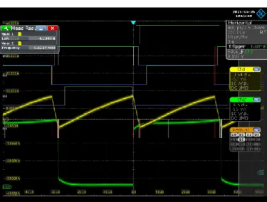
The prototype and the main waveforms obtained are shown in Fig 6. The component description and the theoretical and measured results are summarized in the Table II.
However, the test was done in open loop and the negative current real value was higher than the estimated one. Also the AC resistance of the inductor was higher than the obtained in simulation. Therefore, the Matlab design was recalculated with the actual inductor and negative current as input to the same equations in order compare whether the theoretical result were close to the measured ones and validate the losses estimation models.
With this prototype 99 % efficiency was achieved at nominal conditions. Also, the flying capacitor voltage was half the output voltage without any control loop and ZVS was achieved in all transistors.
V. CONCLUSION
From the optimized models it can be concluded that the main difference between the two converters is that the size of the inductor is decreased if the flying capacitor is included. With appropriate control, both circuits need output voltage sensor and zero current detector, so the control stage will be similar in terms of volume and losses. Regarding the MOSFETs, although the number of transistors is higher in the Flying Capacitor topology, switching losses are similar, since both topologies switch with ZVS. A similar optimization process can be done for any higher number of levels, because increasing the number of levels will decrease the inductor requirements as shown in [5].
The optimization process shows that the Boost with Flying Capacitor has better losses/volume than the Boost for these specifications.
However, the optimization algorithm needs to be further refined in order to get better inductor estimation and the correct value of negative current needed for ZVS.
As it can be seen in table II the theoretical results are close to the prototype results, therefore the losses estimations are valid, with a mismatch of less than 1 % on the efficiency.
REFERENCES
[1] T. Meynard and H. Foch, "Multi-Level Choppers for High Voltage Applications", EPE Journal, vol. 2, no. 1, pp. 45-50, 1992.
[2] Hamidreza Keyhani, Hamid A. Toliyat, “Flying-Capacitor Boost Converter” Advanced Electrical Machines & Power Electronics Lab. Department of Electrical & Computer Engineering Texas A&M University.
[3] U. Drofenik, A. Müsing, and J. W. Kolar, “Voltage-dependent capacitors in power electronics multi-domain simulations", in Proc. 2010 Int.Power Electron. Conf. (ECCE Asia), Sapporo, Japan, Jun. 2010, pp. 643–650.
[4] George G. Orenchak, “Estimating Temperature Rise of Transformer”, TSC Ferrite International. Available:
http://www.tscinternational.com/tech12.pdf
[5] A. B. Ponniran, K. Matsuura, K. Orikawa, and J. Itoh, “Size Reduction of DC-DC Converter using Flying Capacitor Topology with Small Capacitance”, IEEJ Journal of Industry Applications, Vol.3, No.6, pp.446-454 (2014).