Portable low profile antenna at X-band
J.M. Inclán-Alonso*, A. García-Aguilar*, L. Vigil-Herrero*, J.M. Fernández-González*, J. SanMartín-Jara+, M. Sierra-Pérez*
*Radiation Group. Signals, Systems and Radiocommunications Dept. Universidad Politécnica de Madrid. Ciudad Universitaria. 28040. Madrid, Spain.
{ chema, andresg, jmfdez, m.sierra.perez } @gr.ssr.upm.es +Antenas Moyano CO. LTD.
Abstract— An antenna which has been conceived as a portable
system for satellite communications based on the recommendations ITU-R S.580-6 [1] and ITU-R S.465-5 [2]for small antennas, i.e., with a diameter lower than 50 wavelengths, is introduced. It is a planar and a compact structure with a size of 40x40x2 cm. The antenna is formed by an array of 256 printed elements covering a large bandwidth (14.7%) at X-Band with a VSWR of 1.4:1. The specification includes transmission (Tx) and reception (Rx) bands simultaneously. The printed antenna has a radiation pattern with a 3dB beamwidth of 5º, over a 31dBi gain, and a dual and an interchangeable circular polarization.
I. INTRODUCTION
This antenna has been conceived as a portable system for satellite communications based on the recommendations ITUR-S 580-1 and ITUR-S 465-5 for small antennas, i.e., with a diameter lower than 50 wavelengths. The main idea is to have a lightweight antenna that is easy to carry and deploy, very suitable for personal communications.
TABLEI ANTENNA SPECIFICATIONS
Parameter Specification Units
Working bands Tx:
Rx: 7.25 to 7.757.9 to 8.4 GHzGHz Polarization Dual circular
polarizationfor Tx and Rx bands
G/T 7 dB/K
3dB beamwidth 5 degrees Maximum gain 31 dBi
Efficiency >50 % Isolation
between Tx and Rx
>17 dB VSWR 1.4:1
SLL -16 dB
Size 40x40x2 cm
The antenna has a dual circular polarization in TX and Rx bands simultaneously. Thus, all the elements in the antenna have to work in both bands so they have to be designed as wide-band elements.
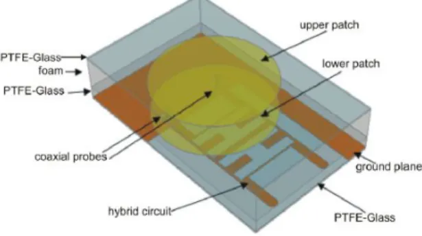
The antenna has been divided in subarrays that can be fabricated separately. Each subarray is connected to a global power distribution network.
II. ANTENNA STRUCTURE
The antenna is formed by array of 16x16 printed elements and covers a large band. The antenna has been divided into 4x4 subarrays, therefore each subarray has 4x4 radiating elements. Subarrays are composed of several layers. The bottom layer is a microstrip network that contains the distribution network for RHCP and LHCP and hybrid circuits to get circular polarization. The upper layers of the subarray contain the double stacked patches.
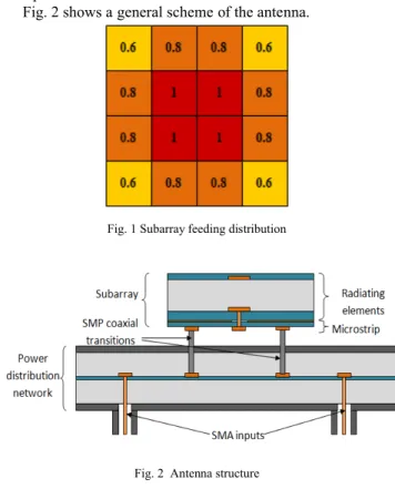
To distribute the power among the subarrays a low losses stripline distribution network is used. In order to get a low side lobes level the subarrays of the corners receive less power that the ones in the center as it can be shown in Fig. 1.
The subarrays are connected to the stripline through SMP-type coaxial connectors. In the power distribution network there are two inputs/outputs in SMA-type connector, one for each polarization.
Fig. 2 shows a general scheme of the antenna.
Fig. 1 Subarray feeding distribution
Fig. 2 Antenna structure
III. RADIATING ELEMENT
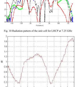
The radiating element is a double stacked circular patch. In order to get a circular polarization the patch is excited by two coaxial probes with orthogonal signals. To provide the antenna with dual polarization in transmission and in reception a hybrid circuit is used. This hybrid circuit is placed in the microstrip layer as is shown in Fig. 3.
Fig. 3 Radiating element schema
Patches are printed in a PTFE_Glass substrate with a permittivity of 2.17. The actives patches are separated from the parasites patches by a thick sheet of foam.
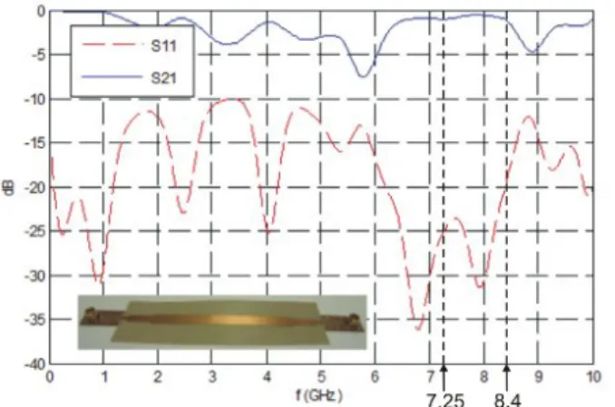
The comparison between the simulated S-parameters and the measured S-parameters at the lower band can be shown in Fig. 5.
(a) (b)
Fig. 4 Test board of the radiating element. (a) Two stacked microstrip patches separated. (b) Feeding network with the SMP-type connectors.
It is important to stress out that due to the behaviour of the hybrid circuit the measured S11 represents the coupling between coaxial probes of each polarization and S21 represents mainly the adaptation of the patch.
The adaptation of the patches is similar to the simulation and the reflection coefficient is lower than -15 dB. We can see that the coupling between polarizations is high in the measures and in the simulation. This is caused by the height of the substrate of the active patches and the coupling between the coaxial probes. This coupling between polarizations can lead to high side lobes level and worse CP/XP ratio. To reduce
the influence of this coupling Willkinson power dividers are used in subarray microstrip network.
Fig. 5 S-Parameter simulated and measured of the radiating element
Fig. 6 shows the measured and simulated radiation pattern. The measured CP/XP ratio is about 21 dB.
Fig. 6 Radiation pattern of the radiating element for LHCP at 7.25 GHz
IV. HYBRID CIRCUIT
There is a hybrid circuit for each element to provide the quadrature signal toward the coaxial probes. The hybrid is the element that enables the antenna to work with a right-handed or a left-handed circular polarization in transmission or in reception. A 3dB branch-line coupler has been chosen as hybrid circuit and, specifically, a periodic branch-line coupler of three branches to get a wide band [2]. But this structure occupies a big volume in the subarray feeding network, therefore it has been necessary to miniaturize the branch-line coupler. A size reduction between 20 to 80% is possible doing the equivalence of a
λ
/4 transmission line to a fractal-shaped line [3], an interdigitally-coupled line [4] or a transmission line with one or more parallel open-ended stubs [5].transmission line to a transmission line with one parallel open-ended stub in order to get the desired bandwidth. This hybrid circuit is shown in Fig. 7. The volume reduction achieved has been of 35%, keeping the behaviour of a conventional periodic 3dB branch-line coupler of three branches.
Fig. 7 miniaturized branch line circuit
The measures of the miniaturized hybrid circuit are shown in Fig. 8. The results are quite good.
Fig. 8 Simulation and measures of the miniaturized branch line
V. SUBARRAY SYSTEM
Each subarray has 4x4 radiating elements separated by 25 mm. The distribution network among the radiating elements is done in microstrip technology. RHCP and LHCP network are implemented in the same layer. The size of the subarrays in the first prototypes is 99x99 mm.
To improve the purity of the polarization the sequential rotation technique is implemented among each 4 elements as it is shown in Fig. 9. Thus, each element is rotated 90º and
excited by a 90º phase-shifted signal compared to the previous one.
(a) (b)
Fig. 9 Test board of the array unit cell formed by 2x2 radiating elements with sequential rotation. (a) Stacked patches separated. (b) Feeding network for
RHCP and LHCP with SMP-type connectors.
The results of a unit cell (2x2 elements) are shown in Fig. 10 and Fig. 11. As we can see the axial ratio is bellow 1.3 dB in X-band.
Fig. 10 Radiation pattern of the unit cell for LHCP at 7.25 GHz
VI. POWER DISTRIBUTION NETWORK
A stripline has been used to distribute the power among the subarrays in order to get a low loss network. The stripline is formed by a metalized line in a thin substrate located between two foam sheets and two plates, which are the ground plane. A quasi-TEM mode is propagated due to the presence of two different dielectrics (PTFE and foam). In order to have a low loss distribution network the height of the foam sheets must be high. The losses in this structure are around 0.6 dB/m which means 0.3 dB of losses in the line.
The transitions between stripline and each subarray are done through SMP type coaxial connectors. The two inputs of the antenna, one for each polarization, are done through SMA type coaxial connectors. To avoid the generation of a TE mode in vertical transitions it is necessary to place a short-ended pseudo-waveguide thereby the TE mode stays as a cut-off mode. The losses for each transition are around 0.3 dB.
The SMP connectors have to be mounted onto a microstrip line. Therefore, a transition between stripline and microstrip line has been designed. The relation between the line width of the stipline and the line width of the microstip line is very big. For this reason the transition has to change gradually the line width as it can be shown in Fig. 12 (a).
(a) (b)
Fig. 12 Transitions from stripline to SMA-type coaxial connector (a) and to SMP-type coaxial connector.
The S-parameters of the transition between the stripline and microstrip are shown in Fig. 13. In the S21 parameter the losses in the two SMP connectors are included.
Fig. 13 S-Parameters of a stripline with SMP transitions
The first prototype of the power distribution network is shown in Fig. 14.
Fig. 14 First prototype of the power distribution network
We have detected some unexpected problems in the prototype of the Fig. 14. The main problem is that a TE resonant mode is excited not only in the vertical transitions but also in other parts of the line. This makes that peaks in the transmission to each subarray appear in some frequencies as we can see in Fig. 15.
Fig. 15 : Measured transmissions of the first prototype of the power distribution network.
To solve this problem a protected stripline network is chosen. This means that the stripline is surrounded by metallic walls. This is easily achieved extending the walls in the transitions. The distance between the walls that shield the line has to be small enough to avoid the propagation of TE modes and large enough to not interfere with the Quasi-TEM mode of the line. A distance of 16 mm is chosen. This distance allows the propagation of TE modes at frequencies above 9 GHz.
Fig. 16 : Protected stripline global distribution network
The results of the transmissions of the power distribution network to the corner subarrays are shown in Fig. 17. The peaks in the transmission have disappeared in the X-band and they only appear in frequencies above 9 GHz (as it has been commented before).
Fig. 17 Measured transmissions of the protected stripline global distribution network
VII. RESULTS
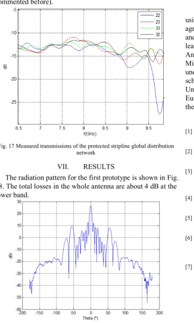
The radiation pattern for the first prototype is shown in Fig. 18. The total losses in the whole antenna are about 4 dB at the lower band.
Fig. 18 Radiation pattern at 7.4 GHz
In the first prototype we have also detected that there are couplings between the polarizations due to the small distance between some lines in the subarray network. For this reason in the second prototype a 3x3 subarray antenna will be implemented, making bigger the size of each subarray.
VIII. CONCLUSIONS
The complete design of a portable printed antenna for satellite communications at X-Band has been introduced. This antenna has been conceived as a planar, compact, modular, low losses and dual circular polarized antenna for Tx and Rx bands simultaneously. First prototype was designed and built successfully. In order to solve some problems detected in the first prototype a second prototype has been designed, the results of this second prototype will be presented at the EuCAP 2011 meating.
ACKNOWLEDGEMENT
The simulations done in this work has been realized using CST Microwave Studio Suite 2010 under a cooperation agreement between Computer Simulation Technology (CST) and Universidad Politécnica de Madrid. The project is leadered by the Universidad PolitÉcnica de Madrid and Antenas Moyano SL and the support of the Spanish Education Ministry (Comisión Interministerial de Ciencia y Tecnología under reference TEC2008-06736/TEC, a Spanish government scholarship (FPI under reference BES-2009-021462), a Universidad Politécnica de Madrid scholarship and the help of European Cost Action IC-0603 Assist. The substrate used in the prototypes was donated by NELTEC S.A.
REFERENCES
[1] ITU-R Recommendation S.580-6 (2004). Radiation diagrams for use as design objectives for antennas of earth stations operating with geostationary satellites.
[2] ITU-R Recommendation S.465-5 (1993), Reference earth-station radiation pattern for use in coordination and interference assessment in the frequency range from 2 to about 30 GHz.
[3] M. Sierra-Castañer, M. Vera-Isasa, M. Sierra-Pérez, J.L. Fernández-Jambrina (2005), Double-Beam Parallel Plate Slot Antenna, IEEE Transactions on Antennas and Propagation, vol. 53, no. 3, pp. 977-984.
[4] G. Matthaei, L. Young, E.M.T. Jones, “Microwave filters, impedance-matching networks, and coupling structures”, Artech House, 1980.
[5] Wen-Ling Chen, Guang-Ming Wang, “Design of Novel Miniaturized Fractal-Shaped Branch-Line Couplers”, Asia-Pacific Microwave Conference, APMC 2007, 11-14 December 2007, pp. 1-3.
[6] Zhiyang Liu, R.M. Weikle, “A Compact Quadrature Coupler Based on Coupled Artificial Transmission Lines”, IEEE Microwave and Wireless Components Letters, vol. 15, no. 12, pp. 889-891, December 2005.