1
About the physical meaning of the critical temperature for
catastrophic optical damage in high power quantum well laser
diodes
J Souto, J L Pura, and J Jiménez
GdS Optronlab, Departamento de Física de la Materia Condensada, Ed. I+D, Universidad de Valladolid, P. de Belén 11, 47011 Valladolid, Spain
E-mail: [email protected]
Short title: About the physical meaning of the critical temperature for catastrophic optical damage
Classification numbers: 02.70.Dh; 42.55.Px; 65.40.De; 68.60.-p
2
Abstract
It is usually assumed that the catastrophic optical damage of high power laser diodes is launched when a critical local temperature (Tc) is reached; temperatures ranging from 120ºC to 200ºC were experimentally reported. However, the physical meaning of Tc in the degradation process is still unclear. In this work we show that, in the presence of a local heat source in the active region, the temperature of the laser structure, calculated using finite element methods, is very inhomogeneously distributed among the different layers forming the device. This is due to the impact that the low dimensionality and the thermal boundary resistances have on the thermal transport across the laser structure. When these key factors are explicitly considered, the quantum well (QW) temperature can be several hundred degrees higher than the temperature of the guides and cladding layers. Due to the size of the experimental probes, the measured critical temperature is a weighted average over the QW, guides and claddings. We show the existence of a great difference between the calculated average temperature, equivalent to the experimentally measured temperature, and the peak temperature localized in the QW. A parallel study on double heterostructure lasers is also included for comparison.
1. Introduction
3
depending on the lasers [1]. Usually, this temperature is measured at the laser front facet; albeit, it has also been measured inside the cavity for lasers showing internal COD [2]. These critical temperatures are surprisingly low, and the understanding about their physical meaning is ambiguous. Furthermore, Tc is considered to be the best parameter to quantify the device resistance to damage [1]. One can summarize that a high Tc is the signature of robust devices, while low Tc is the signature of weak LDs; but, far away from this observation, one cannot argue about the physical mechanism driving the degradation of the laser structure in terms of a physical process, triggered at a so low temperature, enabling the generation of the extended defects responsible of the catastrophic device failure.
The local temperature has been routinely characterized by measuring temperature profiles of the operating devices using a variety of techniques, such as Raman microscopy (µR) [1, 2, 4], thermal
infrared imaging (TII) [2], thermoreflectance (TR) [1-4], and micro-Photoluminiscence (µPL). The
outcome of all these studies is limited by the size of the sampled area, with a lateral resolution slightly submicrometric for the techniques using a focused laser beam, i.e. µR, TR and µPL, and ≈3 µm at the
best for TII. Therefore, the measured temperature is indeed averaged over a region two orders of magnitude larger than the QW thickness in a QW LD. This is very relevant, because the thermal transport across the multilayer structure of the laser renders the temperature distribution around the active region very inhomogeneous.
We present herein a detailed study about the temperature distribution in the active zone of the laser based in the solution of the heat transport equation when a local heat source occurs in the active zone of the laser during operation. We present a comparative analysis between QW and double heterostructure (DH) lasers, showing the relevance of the low dimensionality of the QW in the temperature distribution across the laser structure.
2. Structure of the devices
4
DH laser, whose the active structure consists of a 200 nm thick GaAs layer confined by two Al0.30Ga0.70As 1 µm thick cladding layers. The core of the QW device, which has been described in detail elsewhere [7], consists of a 12 nm thick Al0.10Ga0.90As QW sandwiched in between two 130 nm thick graded barrier layers with aluminum concentrations growing from 0.26 to 0.65, and two cladding layers with 0.65 Al concentration. The substrate, as well as the soldering and heat sink, were chosen identical for both devices. The main parameters used for the calculations were taken from the sources cited in [7].
3. Computational model
The importance of the local QW temperature for the degradation process was highlighted in former works, in which we developed a thermo-mechanical model accounting for the degradation threshold of LDs [7, 9, 10]. In this model, the degradation is originated by a very local heat source in the active layer of the laser, either the QW in QW lasers, or the GaAs layer in DH lasers. This heat source, generated by the accumulation of energy in a defect rich region of the active zone, has been assumed to be uniform for the QW, whereas a Gaussian power distribution has been adopted for the GaAs layer of the DH laser. We are not focusing on the precise physical origin of the initial local heating; it is out of the present scope, though it is a very relevant point to consider in forthcoming works. Here we are dealing with the temperature distribution in the laser structure in the presence of the local heat source. Note that once the heating has started the accumulated heat is mainly due to the laser self-absorption, because of the local bandgap shrinkage. In this work, we solve by finite element methods (FEM) the heat transport equation, aiming to reproduce the temperature distribution in the laser structure induced by the local heat source. Thereafter, one proceeds to evaluate the thermal stresses generated from the inhomogeneous temperature distribution in a structure formed by layers with different properties, both thermal and mechanical. The computations have been performed within the framework of the commercially available program COMSOL Multiphysics®.
[12-5
18] regarding the influence of the layer thickness, the dislocation density and the interface roughness on the thermal conductivity of multilayer structures, all the previous computational studies about the temperature estimation during the operation of the QW LDs have systematically used bulk thermal conductivity figures. We present herein how those contributing factors [19-21] affect the temperature profile across the laser structure, resulting in a highly inhomogeneous temperature distribution around the active zone during the laser operation. Following the expression derived by Liang and Li [19] for the dependence of the thermal conductivity on the thickness of the layers and the roughness of the interfaces, we will show that the Tc usually reported for COD does not meet the true temperature reached in the QW, while it gives a more approximate value to the local temperature in DH lasers.
4. Results and discussion
6
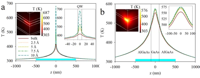
in the QW.Figure 1. Temperature profiles across the growth (z) direction for the studied devices: (a) GRINSCH-QW laser
under a 6 MW/cm2 local heat source, the profiles are calculated for bulk thermal conductivity and for interface
roughness ranging from 2.5 to 10 Å. A more detailed view of the active layers illustrates the progressive
steepness of the temperature gradient in the QW (right insert), whereas a 3D plot with a temperature color code
highlights the dramatic limitation of the heat dissipation from the QW for the 10 Å roughness case (left insert);
(b) DH laser under a local Gaussian distributed heat source, with a 4 MW/cm2 peak value, any other conditions
as in (a). The profiles within the GaAs active layer are shown in the right insert, and the larger extent of the
heating for the 10 Å interface roughness is depicted in the left insert. The origin of the z axis is set at the center
of the QW/GaAs layers. The stripe on the x-axis under the T profiles sets the estimated size of the experimental
probes (about 1 µm). The range in the vertical (z) direction for both left insert images, for which only half of the
structure is depicted (the plane on the right is a symmetry plane), is approximately 1.2 µm.
7
As previously mentioned, the experimentally measured temperature should be the mean value averaged over the different layers simultaneously sampled by the probe beam. In order to confront the calculated data with the usually reported experimental results, we proceed to average the computed temperature distributions over the probe size of the experimental techniques (1µm x 1µm
8
Figure 2. Peak (a) and mean (b) temperatures for the GRINSCH-QW laser as a function of the heat power
density source, and for interface roughness ranging from 2.5 to 10 Å. The computed values assuming bulk
thermal conductivity are included for comparison purposes. Peak (c) and mean (d) temperatures for the DH laser
as a function of the peak heat power density source.
9
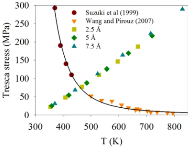
features, were aligned along a straight line, that crosses the experimental curves reported for the yield strength vs T for bulk GaAs at about 480 K. When taking into account the partial suppression of the thermal conductivity, this leads to higher peak temperatures as the interface roughness grows, but the mechanical stresses increase in a correlated manner, so that the Tresca stress - temperature pairs remain all distributed along the same straight line. This is illustrated in Figure 3, where the peak QW T vs Tresca stress computed data are plotted for different values of interface roughness and heat power; the experimental yield strengths for bulk GaAs, as reported in the literature [23, 24], are also depicted. However, our initial estimation was based on peak temperature values, while the experimental Tc reported in the literature correspond to temperatures averaged over the layers surrounding the QW. Assuming QW temperatures of around 500K, the temperature of the adjacent layers is too low to match the experimental data. This suggests the need to reconsider the criterion we followed to define the onset of the mechanical degradation. In fact, we had assumed the starting of the COD to occur when the shear thermal stresses overpass the yield strength of bulk GaAs; however, this approach is probably not fully correct, as one should consider the enhancement of the mechanical strength in nanostructured materials [25-27], which will displace the onset of plasticity of the layers to substantially higher stresses, particularly for the 12 nm QW, while for the DH laser this effect must be significantly less relevant. This point will be treated in forthcoming works.
Figure 3. Experimental yield strengths of bulk GaAs, and calculated peak temperature-Tresca stress pairs for
different interface roughness values. The computed data where evaluated for power densities ranging from 2 to
10
Focusing on the QW laser, more insight into the degradation process can be gathered from Figure 4. This graph represents the computed average temperature versus the QW temperature for various interface roughness values (alternatively, relative amounts of thermal boundary resistance) over an extended power range. The curves for a roughness of 2.5 or 5 Å would correspond to the performance of lasers with the initial QW thermal conductivity [12, 14], if no degradation occurred in the whole temperature range. This is not a realistic assumption, as the elevated peak temperatures reached in the QW would lead to the formation of crystal defects which would lead to increased thermal resistance.
Note that for a given power density, the average temperatures are very similar for the different values of the interface roughness, whereas substantial increments are obtained for the QW temperature due to the increased thermal resistances as the roughness grows. This QW temperature increase will enhance the thermal shear stresses lowering the threshold power for degradation. This mechanism would result in a further decrease of the thermal conductivity, with the concomitant rapid rise of the QW temperature, which could eventually lead to the melting of the QW. Evidence of local melting within the QW has been previously observed for this type of lasers [28].
Figure 4. Average vs peak computed temperatures for the GRINSCH-QW laser, for interface roughness ranging
from 2.5 to 10 Å. Each individual plot represents the calculated values for power densities ranging from 2 to 26
MW/cm2 with 2 MW/cm2 increment steps. The two horizontal lines delimit the experimentally reported Tc
11
The results shown in Figure 4 also reveal a direct connection between the quality of the devices and the (average) critical operation temperature. If, for a given maximum temperature within the QW, one considers the mean value that would be measured on the laser facet, it is clear that the better the thermal conductivity the higher the average temperature estimated for the device. As a matter of fact, if one plots the temperature profiles for similar peak temperatures but for different interface roughness, higher temperature is reached in the guiding and cladding layers when the roughness decreases, which is equivalent to higher Tc, as expected for a more robust device.
5. Conclusions
The thermal distribution due to a local heat source in the active part of a quantum well laser diode has been shown to be very inhomogeneous. We have also demonstrated that the peak temperature is substantially higher than the temperature averaged over the quantum well, the guides and cladding layers; this average temperature can be assimilated to the experimentally measured temperature. In this scenario, the impossibility to directly relate average temperatures to specific physical degradation processes has been addressed, as the physical mechanism driving the degradation seems to be related to the peak temperature in the quantum well, which is significantly higher than the experimentally measured critical temperature.
Acknowledgements
12
REFERENCES
[1] Bettiati M 2013 Microelectron. Reliab.53 1496
[2] Hempel M, Tomm J W, Hortelano V, Michel N, Jiménez J, Krakowski M and Elsaesser T 2012 Laser Photon. Rev.6 L15
[3] Tang W C, Rosen H J, Vettiger P and Webb D J 1991 Appl. Phys. Lett.58 557
[4] Ochalski T J, Pierścińska D, Pierściński K, Bugajski M, Tomm J W, Grunske T and
Kozlowska A 2006 Appl. Phys. Lett.89 071104
[5] Nakwaski W 1990 J. Appl. Phys.67 1659
[6] Smith W R 2000 J. Appl. Phys.87 8276
[7] Martín-Martín A, Avella M, Iñiguez M P, Jiménez J, Oudart M and Nagle J 2009 J. Appl. Phys.106 073105
[8] Menzel U 1998 Semicond. Sci. Technol.13 265
[9] Martı́n-Martı́n A, Avella M, Iñiguez M P, Jiménez J, Oudart M and Nagle J 2008 Appl. Phys.
Lett.93 171106
[10]Martı́n-Martı́n A, Iñiguez M P, Jiménez J, Oudart M and Nagle J 2011 J. Appl. Phys. 110
033113
[11]Fujii H, Ueno Y and Endo K 1993 Appl. Phys. Lett.62 2114
[12]Luckyanova M N, Johnson J A, Maznev A A, Garg J, Jandl A, Bulsara M T, Fitzgerald E A, Nelson, K A and Chen G 2013 Nano Lett.13 3973
[13]Yu X Y, Chen G, Verma A and Smith J S 1995 Appl. Phys. Lett.67 3554
[14]Capinski W, Maris H, Ruf T, Cardona M, Ploog K and Katzer D 1999 Phys. Rev. B59 8105
13
[16]Hopkins P E 2013 ISRN Mech. Eng. DOI 10.1155/2013/682586
[17]Cheaito R, Duda J C, Beechem T E, Hattar K, Ihlefeld J F, Medlin D L, Rodriguez M A, Campion M J, Piekos E S and Hopkins P E 2012 Phys. Rev. Lett.109 195901
[18]Zou J, Kotchetkov D, Balandin A A, Florescu D I and Pollak F H 2002 J. Appl. Phys.92 2534
[19]Liang L H and Li B 2006 Phys. Rev. B73 153303
[20]Chen G. and Tien C L 1993 J. Thermophys. Heat Transf.7 311
[21]Ziambaras E and Hyldgaard P 2006 J. Appl. Phys.99 054303
[22]Gesikowska E and Nakwaski W 2008 Opt. Quant. Electron.40 205
[23]Suzuki T, Yasutomi T, Tokuoka T and Yonenaga I 1999 Philos. Mag. A 79 2637
[24]Wang S and Pirouz P 2007 Acta Mater.55 5500
[25]Gerberich W W, Michler J, Mook W M, Ghisleni R, Östlund F, Stauffer D D and Ballarini R 2009 J. Mater. Res.24 898
[26]Michler J, Wasmer K, Meier S, Östlund F and Leifer K 2007 Appl. Phys. Lett.90 043123
[27]Zhu T and Li J 2010 Prog. Mater. Sci.55 710