Universidad de
Valladolid
E.T.S.I. Telecomunicación
Trabajo Fin de Grado
Grado en Ingenierías Específicas de
Telecomunicación, Mención en Telemática
Design and implementation of a standalone
CNC controller
Ontwerp en implementatie van een stand-alone
CNC-besturingseenheid
Autor:
Elias Verstappe
Tutor de UVa:
Dr. Jesús M. Hernández Mangas
Tutor de Universidad Vives (Brugas, Bélgica):
Mr. Tom Cordemans
Title:
Design and implementation of a standalone
CNC controller
Author:
Elias Verstappe
Tutor:
Dr. Jes´
us M. Hern´
andez Mangas
Department:
Department of Electronics
Court
Chairman:
Dr. Mart´ın Jara´ız Maldonado
Member:
Dr. Jes´
us Arias ´
Alvarez
Secretary:
Dr. Jes´
us M. Hern´
andez Mangas
Substitute:
Dr. Ruth Pinacho
Substitute:
Dr. Pedro L´
opez
Date:
21 of June 2019
Preface and acknowledgements
Writing a thesis is the final step in obtaining a degree. It is a unique opportunity to apply all acquired knowledge in one large project. Obviously, the development of such a project does not go without a hitch. It is a mountain that is impossible to get over without falling and getting back up. I would not have succeeded without a strong start and necessary support along the way. Therefore I would like to use this opportunity to express my gratitude to the people who have contributed to the realization of this work.
Therefore, first of all, a sincere thanks to my teachers. Your motivated, enthusiastic and communica-tive way of working and your course of action is a permanent source of inspiration for me.
In addition, a special thanks goes to my internship promoter, Mr. Tom Cordemans. Thank you for the practical support (in connection with Erasmus) and the confidence that you have placed in me from the start. This thesis would not have been realised without your help.
An additional word of thanks goes out to my two promoters at the University of Valladolid, Dr. Jesús M. Hernández Mangas and Dr. Jesús Arias Álvarez. Day after day you have guided me and at the moments that I started going on the wrong path, your expertise broadened my field of vision.
Finally, I want to thank my parents. You have supported me from the beginning. Not just morally and financially, but in many other areas. Thank you for supporting my choice of studying electronics.
Abstract
English
This bachelor thesis has been developed by Daan Ver Eecke and Elias Verstappe. We are two students at the ‘Hogeschool Vives’ in Bruges (Belgium) and both participate in the Erasmus program. The thesis has been worked out at the University of Valladolid in Spain.
The general purpose of a bachelor’s thesis is to solve a specific problem (in our case with regard to the field of study electronics).
This thesis describes how we control an old machine with the help of modern electronics. In a world where technological development is happening faster than ever, it is important that the possibility re-mains to control old devices. Due to the enormous growth, older machines are no longer supported by new operating systems.
Two lecturers from the University of Valladolid, Dr. Jesús M. Hernández Mangas and Dr. Jesús Arias Álvarez, have confronted us with the following challenge: an old CNC machine is currently controlled with the help of an old computer. The program that controls the machine runs on the MS-DOS operating system. Our assignment is to design a custom controller that takes over the task of the old computer. An additional requirement is to also be able to control the (CNC) machine via a website.
A fully custom printed circuit board is designed to solve this problem. The firmware that is responsible for all control is also developed by us. Briefly summarized, the requirements are the following:
With the help of an SD card, a certain PCB design can be read in the machine. The machine can be controlled in two ways: on the one hand everything can be operated using the touchscreen, and on the other hand the machine must be able to be fully controlled via a website.
Now that the project is finished, we can conclude that thanks to the enormous development of tech-nology in recent years, nowadays you can easily and cheaply design a control unit for old devices. We can simulate the operation of a computer that is 25 years old with a small and simple printed circuit board that costs 45 euros (development costs not included).
Dutch
Deze bachelor-thesis is uitgewerkt door Daan Ver Eecke en Elias Verstappe. Wij zijn twee studenten aan de ‘Hogeschool Vives’ in Brugge (België) en nemen beiden deel aan het Erasmus-programma. De thesis is uitgewerkt aan de Universiteit van Valladolid in Spanje.
Het algemene doel van een bachelor proef is om een concreet probleem (in ons geval met betrekking tot de afstudeerrichting elektronica) op te lossen.
Dit eindwerk beschrijft hoe we een oude machine aansturen met behulp van moderne elektronica. In een wereld waar de technologische ontwikkeling sneller dan ooit verloopt, is het belangrijk dat de mogelijkheid blijft bestaan om oude toestellen aan te sturen. Door de enorme groei worden oudere machines niet meer ondersteund door nieuwe besturingssystemen.
Twee docenten van de Universiteit van Valladolid, Dr. Jesús M. Hernández Mangas en Dr. Jesús Arias Álvarez, hebben ons voor de volgende uitdaging geplaatst: een oude CNC-machine wordt mo-menteel bestuurd met behulp van een oude computer. Het programma die de machine bestuurt draait op het MS-DOS besturingssysteem. Het is onze opdracht om een op maat gemaakte controller (bestur-ingseenheid) te ontwerpen, die de taak van de oude computer overneemt. Een extra vereiste is om de (CNC-) machine ook via een website te kunnen besturen.
Om dit probleem aan te pakken en op te lossen wordt een volledig op maat gemaakte printplaat ont-worpen. De firmware die verantwoordelijk is voor alle sturing wordt ook door ons ontwikkeld. Kort samengevat zijn de vereisten de volgende:
Met behulp van een SD-kaart kan een bepaald PCB-ontwerp in de machine gelezen worden.
De besturing van de machine kan op twee manieren: enerzijds kan alles bediend worden met behulp van het touchscreen, anderzijds moet de machine volledig bestuurd kunnen worden via een website.
Nu het project uitgewerkt is kunnen we besluiten dat je dankzij de enorme ontwikkeling van de tech-nologie, vandaag gemakkelijk en goedkoop een besturingseenheid kan ontwerpen voor oude toestellen. Wij kunnen nu de werking van een computer die 25 jaar oud is nabootsen met een klein en simpel print-plaatje dat 45 euro kost (ontwikkelingskost niet inbegrepen).
Contents
1 Introduction 1
1.1 Definition of terms . . . 1
1.2 Statement of the problem . . . 1
1.3 Description of the chapters . . . 2
1.4 Requirements and specification . . . 2
2 Hardware 3 2.1 Used software . . . 3
2.2 Design approach . . . 3
2.2.1 Power supply . . . 4
2.2.2 USB to UART converter and switch between controllers . . . 5
2.2.3 Microcontroller . . . 6
2.2.4 TFT shield . . . 7
2.2.5 Parallel port . . . 9
2.3 The layout . . . 10
2.4 Power analysis . . . 12
2.5 Heat dissipation . . . 13
3 Firmware 14 3.1 Tasks of the microcontroller . . . 15
3.1.1 Detailed description . . . 15
3.1.2 Screen handler . . . 16
3.2 LCD screen . . . 18
3.2.1 Pixel . . . 18
3.2.2 Line . . . 18
3.2.3 Bresenham’s line algorithm[3] . . . 19
3.2.4 Character and string . . . 20
3.3 Touch control . . . 22
3.3.1 Calibration[5] . . . 22
3.4 Interfacing with the machine . . . 23
3.4.1 Pressing a button . . . 23
3.4.2 Checking if a spot is touched . . . 24
3.5 Control the CNC machine . . . 25
3.5.1 CNC routines . . . 25
3.5.2 Speed up and slow down . . . 25
3.5.3 Move the head . . . 26
3.5.4 Circular buffer[7] . . . 27
3.6 Read SD-card . . . 28
3.6.1 Read contents of a file . . . 28
3.8.3 Transmission . . . 35
3.8.4 Reception . . . 35
4 User manual 36 4.1 Start up / main screen . . . 36
4.2 Configuration . . . 38
4.3 Tools . . . 39
4.4 Offset . . . 40
4.5 Load and Start . . . 41
5 Cost study 43 5.1 Material . . . 43
5.2 Labour . . . 45
5.3 Total . . . 45
6 Conclusions 46
Bibliography 47
A PCB schematic 49
B PCB Layout 56
C Bill of materials 62
D Design errors 64
E Explanation of calibration in touchscreen systems 66
List of Figures
1.1 Project definition . . . 1
2.1 Simplified hardware schematic . . . 3
2.2 Power supply . . . 4
2.3 Switch between controllers for programming . . . 5
2.4 The microcontrollers memory map . . . 6
2.5 Four-wire touch screen circuit . . . 7
2.6 Four-wire touch screen construction . . . 7
2.7 Pins related to the TFT shield . . . 8
2.8 Resistor devider for level conversion . . . 9
2.9 Antenna copper cutout . . . 10
2.10 Copper heat plane connected to 3V3 pin . . . 10
2.11 Real board top view . . . 11
2.12 Real board bottom view . . . 11
3.1 Connections and associated protocols . . . 14
3.2 Main function . . . 15
3.3 Processing the displays . . . 17
3.4 Result of Bresenham’s line algorithm . . . 19
3.5 Closup of figure 3.4 . . . 19
3.6 ‘a’ character bitmap . . . 20
3.7 ‘Line feed’ and a ‘carriage return’ . . . 21
3.8 Example graphic . . . 21
3.9 Difference in coordinates . . . 22
3.10 Circle transformation due to misalignment and scaling . . . 22
3.11 Touching a button . . . 23
3.12 Perform an action when button is touched . . . 24
3.13 Error margin . . . 24
3.14 ‘Touch’ in idle state . . . 24
3.15 Circular buffer - setParam_cmd command . . . 26
3.16 No free entries in the buffer (left) and entries can be filled (right) . . . 27
3.17 Select file procedure . . . 28
3.18 Flowchart explaining how an HPGL file is processed . . . 30
3.19 Flowchart explaining how an excellon file is processed . . . 32
3.20 Frame format . . . 34
3.21 Frame filled with tools data . . . 34
3.22 State machine that processes the incoming frame . . . 35
3.23 Full description of the tools payload . . . 35
4.1 Main screen . . . 36
4.8 Inactive and active start button . . . 41
4.9 Machine is running . . . 42
4.10 Pup-up for tool change . . . 42
B.1 Real board top view . . . 60
B.2 Real board bottom view . . . 61
D.1 Faulty connection . . . 64
D.2 Error has been fixed . . . 64
D.3 Faulty reset connection . . . 64
D.4 Reset connected to 5V . . . 64
D.5 Solution for the design error regarding the 40-pin header . . . 65
List of Tables
2.1 Table with currents drawn by each component . . . 12
2.2 Table with heat dissipated by each component . . . 13
5.1 Bill of materials, part 1 . . . 43
5.2 Bill of materials, part 2 . . . 44
List of abbreviations and symbols
ARM Advanced RISC machine[1]
ASCII American standard code for information interchange
CNC (machine) Computer numerical control (machine)
FAT File allocation table
HPGL Hewlett-Packard Graphics Language
IC Integrated circuit
LCD Liquid crystal display
MCU Microcontroller unit
MISO Master in slave out
MOSI Master out slave in
PCB Printed circuit board
PFF Petit FAT filesystem
SMD Surface-mounted device
Chapter 1
Introduction
1.1
Definition of terms
This final settlement was an exam. The comments made during the defence were not included.
This bachelor’s thesis was elaborated by Daan Ver Eecke and Elias Verstappe. We are two Belgian students from ‘Hogeschool Vives, campus Bruges Station’. We study ‘electronics’, which is part of the applied engineering and technology field of study. Our mentor from our university in Belgium is Mr. Tom Cordemans. Our two mentors from the University of Valladolid are Dr. Jesús M. Hernández Mangas and Dr. Jesús Arias Álvarez.
This study contains information about the hardware development and firmware that controls the CNC machine. This study was written by Elias Verstappe. Alongside this project, a website was made to control the CNC machine. You can read about the development of the website and the drawing of the 3D printed case in the study that Daan Ver Eecke wrote.
1.2
Statement of the problem
The main goal of a bachelor’s thesis is to solve a specific problem, with regards to the field of study. Two professors from the University of Valladolid have given us the following problem to solve:
An old CNC machine that is used to manufacture printed circuit boards, is currently controlled by an old personal computer. The communication is done via the parallel port and the application to control the machine runs on the MS-DOS operating system. It is our task to design a controller that controls the CNC machine. This should be done by designing a custom printed circuit board (PCB).
x y
z
CNC - machine
Personal computer (MS-DOS) parallel
port
O
ld
s
y
s
te
m
x y
z
CNC - machine
New system
Touch panel
STOP
Our controller
wall mount USB power SD card
slot
WiFi interface
1.3
Description of the chapters
Chapter 1 has a detailed description of the specific requirements that were set when the idea of this thesis was developed.
Chapter 2describes the specific details about the PCB design.
InChapter 3you can read about the firmware that manages the various tasks the controller has.
Furthermore, Chapter 4is a user manual that describes all parameters that can be set and describes
how the ‘operating system’ that runs on the board works.
Chapter 5gives you an idea of how much the development this project would cost.
Finally,Chapter 6contains conclusion of the final work and discusses the achieved results.
1.4
Requirements and specification
Specific requirements of the project are the following:
• The controller needs to operate fully independently, no computer will be required when using the CNC machine.
• The design that you wish to manufacture by the CNC machine is supplied to the controller via an SD card.
• The (CNC) machine should be fully controllable using a web page. • The (CNC) machine should be fully controllable via a touchscreen.
Chapter 2
Hardware
2.1
Used software
The software that was used to develop the PCB is Proteus Design Suite. This software tool is used to design and develop schematics for PCB’s. It was developed by Labcenter Electronics Ltd. One of the reasons why Proteus was used is that we can easily simulate our design on the computer. This is useful, reason being that we can already start writing firmware for the design while we wait for the manufacturer to develop our circuit board.
2.2
Design approach
Figure 2.1 gives you a closer look at how the circuit board is designed and shows which components are present. The following subsections describe the major parts of the board.
We need specific hardware to meet the requirements. A list of all integrated circuits (IC’s) and other components can be found in the bill of materials, which is one of the appendices of this study.
USB to UART (FT232RL)
MCU (LPC2106)
SD card
Touch panel (XPT2046)
Display control (SSD1963) TFT shield
I/O expander
(MCP23S17)
Parallel port
WiFi module (ESP8266)
Switch
USB
5V 1V8
Data 3V3
3V3
4
0
p
in
h
e
a
d
e
r
Level converter
(74HCT04D)
5V 5V
3V3
3V3 1V8
3V3 > 1V8
(MC33375)
5V > 3V3
(TC2117) 3V3
Power
2.2.1
Power supply
Power is provided by the USB connection. Our circuit uses both 5V and 3,3V as well as 1,8V. The 5V is directly derived from the USB connection, the 3,3V and 1,8V are achieved by using voltage regulators. Specific design can be found in the PCB layout, which is included as an appendix.
Every power rail is connected to ground via a capacitor of 22µF. The datasheet suggest that we use
10µF capacitors, but for stock reasons 22µF capacitors were used. This has no negative effect on the
working of the power supply.
With the help of two voltage regulators the voltage is converted from 5V to 3,3V and then from 3,3V to 1,8V. The figure below shows how this was implemented.
Figure 2.2: Power supply
You may have noticed that there is another component between the power supply of the USB con-nector and the 5V power rail (component L1). This is a ferrite bead. A ferrite bead[2] is an electric component that suppresses high-frequency noise in electronic circuits. No safety measures have been taken in connection with a potential electrostatic discharge. This is not the main focus of this study and we do not expect problems in that regard.
2.2.2
USB to UART converter and switch between controllers
The microcontroller (when ‘the microcontroller’ is used, I’m refering to the LPC2106) and WiFi module will be programmed via USB. The board will also be powered via USB. A USB to UART converter is needed to be able to communicate with the microcontroller and WiFi-module.
We only want to use one USB to UART converter (and one USB connection). To be able to choose which microcontroller we program, we use a switch. The schematic below gives a clearer view of how these parts are connected. This can also be found in the schematic itself, which is one of the appendices.
TXD
RXD
USB to UART
D-D+
FT232RL
RxD0
TxD0
(P0.1)(P0.0)
Microcontroller
TxD1
RxD1
(P0.8)(P0.9)
LPC2106
TXD
RXD
WiFi module
ESP8266
1 2 3
4 5 6
U
S
B
_
T
X
D
U
S
B
E
S
P
_
R
X
D
E
S
P
T
x
D
R
x
D
0
Figure 2.3: Switch between controllers for programming
When the slide switch is in one position, the converter’s transmit signal is connected to the
micro-controller’sreceivepin. Also, the converter’sreceive signal is connected to the microcontroller’stransmit
pin. This results in data communication between converter and microcontroller. When the switch is in the other position, data is beeing shared between the converter and the WiFi module.
You can also see that the WiFi modules UART interface is connected to the second UART interface of the microcontroller. This connection is present because we need to be able to control the CNC machine via a website. Because the microcontroller is responsible for the management and control of the CNC machine, the WiFi module has to tell the main microcontroller what the user wants to do.
2.2.3
Microcontroller
The microcontroller that we use is an LPC2106/01. This is an ARM based microcontroller (or MCU). We chose this controller because we have experience using it and the lecturers who developed the idea of this project can help us during development if any major problems would arise.
The microcontroller runs on a frequency of approximately 58,98 MHz. In our application, this frequency is achieved by a clock crystal that produces a frequency of 14,7456 MHz, which is then multiplied by four using a PLL.
In figure 2.4 we can see that our microcontroller has 64kB or RAM memory and 128kB of flash memory.
1. Memory map
The LPC2104/05/06 incorporates several distinct memory regions, shown in the following
figures.
shows the overall map of the entire address space from the user
program viewpoint following reset. The interrupt vector area supports address remapping,
which is described later in this section.
UM10275
Chapter 2: LPC2104/05/06 memory addressing
User manual
AHB PERIPHERALS
APB PERIPHERALS
RESERVED ADDRESS SPACE
BOOT BLOCK (RE-MAPPED FROM ON-CHIP FLASH MEMORY
RESERVED ADDRESS SPACE
16 kB ON-CHIP STATIC RAM (LPC2104) 32 kB ON-CHIP STATIC RAM (LPC2105) 64 kB ON-CHIP STATIC RAM (LPC2106)
RESERVED ADDRESS SPACE FAST GPIO REGISTERS(1)
128 kB ON-CHIP FLASH MEMORY
0xFFFF FFFF
0xF000 0000 0xEFFF FFFF
0xE000 0000
0xC000 0000 0xDFFF FFFF
0x8000 0000 0x7FFF FFFF
0x7FFF E000 0x7FFF DFFF
0x4000 4000 0x4000 3FFF 0x4000 8000 0x4000 7FFF 0x4001 0000 0x4000 FFFF
0x4000 0000 0x3FFF FFFF 0x3FFF C000
0x0002 0000 0x0001 FFFF
0x0000 0000 4.0 GB
3.75 GB
3.5 GB
3.0 GB
2.0 GB
1.0 GB
0.0 GB
2.2.4
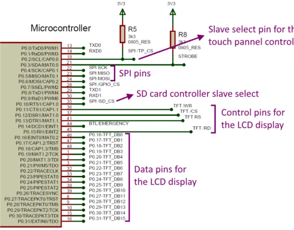
TFT shield
The TFT shield contains three controllers, one is responsible for the touch management. The second one is responsible for controlling the LCD screen and the last one is the SD card itself. Given that these chips (and SD card slot) were already integrated on the shield, we didn’t have to design anything special for this part of our PCB. We only need to correctly connect the pins from the 40 pin connector to the microcontroller.
Touch controller
The touchscreen is controlled by the XPT2046 IC. This chip communicates with the microcontroller via SPI. The IC controls a resistive touch screen. A resistive touch screen works by applying a voltage across a resistor network and measuring the change in voltage at a given point on the matrix where a screen is touched by an input stylus, pen or finger. The change in the resistance ratio marks the location on the touch screen.
®
©2000 Burr-Brown Corporation AB-158 Printed in U.S.A. April, 2000
TOUCH SCREEN CONTROLLER TIPS
By Skip Osgood, CK Ong, and Rick Downs
Burr-Brown makes a number of specialized analog-to-digi-tal converters for touch screen applications. The ADS7843, ADS7845, and the new ADS7846 converters all are de-signed for specific touch screen applications. Applications using these devices can benefit greatly from the tips pre-sented in this application bulletin. Most of the examples discuss the ADS7843, but the techniques shown are appli-cable to all of the devices.
We begin by looking at the theory of operation of a resistive touch screen, and using these specialized A/D converters with such a screen. Techniques are presented for improving accuracy and minimizing errors; the operation of the pen interrupt line (PENIRQ) is explored, ESD protection meth-ods for the converters, and issues surrounding interfacing these converters to popular microprocessors are discussed.
RESISTIVE TOUCH SCREENS
A resistive touch screen works by applying a voltage across a resistor network and measuring the change in resistance at a given point on the matrix where a screen is touched by an input stylus, pen, or finger. The change in the resistance ratio marks the location on the touch screen.
The two most popular resistive architectures use 4-wire or 5-wire configurations (as shown in Figure 1). The circuits determine location in two coordinate pair dimensions, al-though a third dimension can be added for measuring pres-sure in 4-wire configurations.
THE 4-WIRE TOUCH SCREEN COORDINATE PAIR MEASUREMENT
A 4-wire touch screen is constructed as shown in Figure 2. It consists of two transparent resistive layers.
The 4-wire touch screen panel works by applying a voltage across the vertical or horizontal resistive network. The A/D converts the voltage measured at the point the panel is touched. A measurement of the Y position of the pointing device is made by connecting the X+ input to a data converter chip, turning on the Y+ and Y– drivers, and digitizing the voltage seen at the X+ input. The voltage
FIGURE 1. 4-Wire and 5-Wire Touch Screen Circuits.
Four-Wire Five-Wire Conductive Bar Insulating Material (Glass) Silver Ink Transparent Conductor (ITO) Bottom Side Transparent Conductor (ITO) Top Side X+ X– Y+ Y–
ITO = Indium Tin Oxide
FIGURE 2. 4-Wire Touch Screen Construction.
SBAA036
Figure 2.5: Four-wire touch screen circuit
Our touch screen is based on the ‘four-wire’ architecture. A four-wire touch screen is constructed as shown in figure 2.6. It consists of two transparent resistive layers. The four-wire touch screen panel works by applying a voltage across the vertical or horizontal resistive network. The A/D converts the voltage measured at the point the panel is touched. A measurement of the Y position of the pointing device is made by connecting the X+ input to a data converter chip, turning on the Y+ and Y- drivers and digitizing the voltage seen at the X+ input. The voltage measured is determined by the voltage divider developed at the point of touch. For this measurement, the horizontal panel resistance in the X+ lead doesn’t affect the conversion due to the high input impedance of the A/D converter. Voltage is then applied to the other axis, and the A/D converts the voltage representing the X position on the screen through the Y+ input. This provides the X and Y coordinates to the associated processor.
®
TOUCH SCREEN CONTROLLER TIPS
By Skip Osgood, CK Ong, and Rick Downs
Burr-Brown makes a number of specialized analog-to-digi-tal converters for touch screen applications. The ADS7843, ADS7845, and the new ADS7846 converters all are de-signed for specific touch screen applications. Applications using these devices can benefit greatly from the tips pre-sented in this application bulletin. Most of the examples discuss the ADS7843, but the techniques shown are appli-cable to all of the devices.
We begin by looking at the theory of operation of a resistive touch screen, and using these specialized A/D converters with such a screen. Techniques are presented for improving accuracy and minimizing errors; the operation of the pen interrupt line (PENIRQ) is explored, ESD protection meth-ods for the converters, and issues surrounding interfacing these converters to popular microprocessors are discussed.
RESISTIVE TOUCH SCREENS
A resistive touch screen works by applying a voltage across a resistor network and measuring the change in resistance at a given point on the matrix where a screen is touched by an input stylus, pen, or finger. The change in the resistance ratio marks the location on the touch screen.
The two most popular resistive architectures use 4-wire or 5-wire configurations (as shown in Figure 1). The circuits determine location in two coordinate pair dimensions, al-though a third dimension can be added for measuring pres-sure in 4-wire configurations.
THE 4-WIRE TOUCH SCREEN COORDINATE PAIR MEASUREMENT
A 4-wire touch screen is constructed as shown in Figure 2. It consists of two transparent resistive layers.
The 4-wire touch screen panel works by applying a voltage across the vertical or horizontal resistive network. The A/D converts the voltage measured at the point the panel is touched. A measurement of the Y position of the pointing device is made by connecting the X+ input to a data converter chip, turning on the Y+ and Y– drivers, and digitizing the voltage seen at the X+ input. The voltage
FIGURE 1. 4-Wire and 5-Wire Touch Screen Circuits.
Four-Wire Five-Wire Conductive Bar Insulating Material (Glass) Silver Ink Transparent Conductor (ITO) Bottom Side Transparent Conductor (ITO) Top Side X+ X– Y+ Y–
ITO = Indium Tin Oxide
FIGURE 2. 4-Wire Touch Screen Construction.Figure 2.6: Four-wire touch screen construction
The touch screen is used in differential mode. This basically means that any variation in the touch panels resistance due to change in power supply, changes in driver impedance or changes in temperature will be compensated for by the ratiometric operation of the A/D converter. We use differential mode, as opposed to single-ended mode, because it is more accurate.
LCD screen
The screen is connected to the microcontroller using sixteen data lines, one read and one write line, a
reset line anda chip select line. Data is sent to the LCD screens controller using the sixteen data lines.
For colors, only sixteen bits are used, the RGB565 color representation is used for this. This basically means that five data lines are used for the red pixels, six for the green pixels and the five remaining ones are used for the blue pixels. This was done to be able to send the color of one pixel at once, in stead of splitting this process into multiple data transfers. The result is a faster data rate which helps with the responsive feeling and fast working of the screen.
SD card
The SD card communicates with the microcontroller via SPI.
Figure 2.7: Pins related to the TFT shield
2.2.5
Parallel port
I/O expanderThe output of the parallel port is controlled through the I/O expander. We use the MCP23S17 IC. The reason why the parallel port wasn’t directly connected to the microcontroller is that we don’t have enough I/O pins to our disposal. The microcontroller communicates with the I/O expander via SPI. The I/O expander then controls the pins of the parallel port. Data coming from the CNC machine itself is sent to the microcontroller via the same SPI interface.
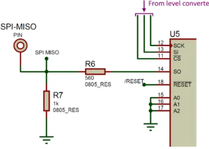
Level converter
As a result of using the I/O expander and because the parallel port needs to be 5V logic, we need a ‘level converter’. The microcontroller works at a voltage level of 3,3V. The I/O expander works with 5V logic. We fixed this problem by placing an integrated circuit that sees a 3,3V signal as a logical ‘1’ between the microcontroller and the I/O expander. The integrated circuit we use is a 74HCT04. This is an inverter circuit that contains six NOT gates. Both the SPI clock and SPI MOSI are connected to the I/O expander via two NOT gates (inverting twice results in the same signal, if we ignore the propagation delay). The two remaining NOT gates are each connected to a different signal, one is connected to the ‘chip select’ (slave select) pin. The last one is connected to the ‘strobe’ pin. The strobe signal has its own dedicated pin because we need very precise control over this signal. It is connected directly to the microcontroller. A final point to take into account is the MISO signal. The pins of the microcontroller are 5V tolerant, but the MISO pin is also connected to other integrated circuits that are not 5V tolerant (for example the touch panel controller or the SD card). For this reason, the signal must be converted from a 5V signal to a 3,3V signal. You can see that this is done by using a simple voltage divider in figure 2.8.
Figure 2.8: Resistor devider for level conversion
When the I/O expanders ‘slave out’ pin is high (5V), the voltage found on the ‘SPI-MISO pin’ can be calculated as follows:
VSP I−M ISO= R6
(R6+R7)
∗VSO
VSP I−M ISO=
1kΩ
(560 + 1kΩ)∗5V
2.3
The layout
We managed to use a two layer PCB. This means that conductors are only present on the top and bottom side of the circuit board, in contrast to a more-than-two layered design, where additional layers are inside of the board. Most components are SMD components. The only through-hole components that are used are connectors such as the 40-pin header and the 25-pin SUBD connector.
The schematic itself can be found in appendix B. Figures of the real board can be found on page 11.
We took some options into consideration when placing the components are the following facts: • All connectors (USB and SUBD) are placed at the edge of the PCB, such that you can easily
connect a cable to it.
• Decoupling capacitors are placed as close as possible to the components.
• The button is placed where it is, so that it is located in the centre line of the screen.
• The 40 pin header is placed on the side so that the centre of the TFT shield is as close to the centre of the main PCB as possible.
• As the datasheet for the WiFi module suggests, it is advised to have no copper under and around the antenna. In this figure you can see that no copper can be found under the antenna and 15mm from the edge of the board.
Daan Ver Eecke Elias Verstappe
CNC controller
This project is a colaboration between
&
Daan Ver Eecke Elias Verstappe
CNC controller
This project is a colaboration between
&
Daan Ver Eecke Elias Verstappe
CNC controller
This project is a colaboration between
&
Figure 2.9: Antenna copper cutout
Figure 2.11: Real board top view
2.4
Power analysis
To power our PCB we use a micro USB a mini USB type B connection. These USB connections provide a voltage of 5V with a maximum current of 0,5A. This equals a power of 2,5W.
5V power level 3,3V power level 1,8V power level
40µA (level-converter) 15mA (USB to UART converter) 35mA (microcontroller)
2mA (I/O expander) 200mA (TFT)
420.2mA (3V3) 170mA (WIFI module)
130µA (3V3 regulator internal) 35mA (1V8)
200µA (1V8 regulator internal)
TOTAL @ 5V = 422.37mA TOTAL @ 3V3 = 420.2mA TOTAL @ 1V8 = 35mA
POWER @ 5V = 2.12W POWER @ 3V3 = 1.39W POWER @ 1V8 = 0.063W
Table 2.1: Table with currents drawn by each component
We have three voltage levels in our design: 1,8V, 3,3V and 5V. There is only one component connected to the 1.8V level, this is the LPC2106 (microcontroller). The microcontroller consumes a maximum of 35mA. We can now calculate the required power for the 1,8V power level.
P =U∗I= 1,8V ∗0,035A= 0,063W = 63mW
The 3,3V power rail is connected to three components, but we have to take five currents into account. The three components connected to the 3,3V level are the USB to UART converter, the TFT module and the WiFi interface. These consume 15mA, 200mA and 170mA respectively. The current needed in for 1,8V circuit also has to pass through the 3,3V regulator. We also have to take this current into account to calculate the maximum current draw fot the 3,3V power level. Together we get a total of 420,2mA for the 3,3V power level. The power used for this power level can be calculated as follows:
P=U∗I= 3,3V ∗420,2mA= 1,39W
Our PCB is powered by the USB cable which provides a voltage of 5V. There are only two
compo-nents connected to the 5V level, the level converter, which consumes 40µA and the I/O expander which
consumes 2mA. We also have to take into account the current used by the 3,3V level. That is 420,2mA.
e also need a current of 130µA to power the electronics inside of the 3,3V voltage regulator. If we add
all of these currents together, we get a total current of 422,37mA in for the 5V level. With these values we can calculate the power used by the entire PCB.
2.5
Heat dissipation
It is very important to perform a heat dissipation analysis on the PCB. If the heat analysis indicates that a component may overheat, then we should consider using a heatsink. In our project the two voltage regulators have the biggest chance to overheat.
Component IC code Max. temp [°C] Conditions
Microcontroller LPC2016 85 IDD = 45mA @ 60MHz
USB to UART FT232RL 85 /
16 bit I/O expander MCP23S17 125 /
Level-converter 74HCT04D 70 Above 70°CPtot
(NOT port) drops 8mW/K
Wifi interface ESP-12F 125 Operating temp.
1V8 voltage regulator MC33375ST-1.8T3G RθJ A = 80°C/W,
125°C /
3V3 voltage regulator TC2117-3.3VDBTR RθJ A = 59°C/W,
125°C /
Table 2.2: Table with heat dissipated by each component
3,3V voltage regulator
The datasheet of the TC2117-3.3VDBTR (3,3V voltage regulator) indicates that the thermal resistance between the junction and the air equals 59°C/W. On the basis of our power analysis we know that the current through the 3,3V regulator is 420,2mA. We can determine the drop-off voltage by subtracting the output voltage from the input voltage.
= (5V −3,3V) = 1,7V
Now we can calculate the power generated in the 3V3 regulator. If we then multiply this result with the thermal resistance we get the temperature that the component reaches.
420,2mA∗(5V −3,3V)∗59°C
W + 25°C= 67,15°C
1,8V voltage regulator
The generated heat who this component will emit can be calculated in the same way as shown above.
The datasheet of the MC33375ST-1.8T3G(1V8 regulator) indicates that the thermal resistance (RθJ A) is
80°C/W. We can use the same method as with the 3V3 regulator to calculate the stationary temperature.
35mA∗(3V3−1V8) = 0,0525W ∗80°C
W + 25°C= 29,2°C
Chapter 3
Firmware
There are two microcontrollers on the circuit board. One of them controls the screen and CNC machine itself, the other is responsible for the WiFi integration of the controller. The following sections provide information about the firmware that was written for the main microcontroller (LPC2106). The diagram below shows which components are connected to each other and how they communicate with each other.
USB to
UART
MCU
(LPC2106)
SD card
Touch
panel
Display
control
SPI
SPI
20 /
TFT shield
I/O
expander
Parallel
port
SPI 16
/
/ 1
WiFi module
(ESP8266)
UART UART
UART Switch
USB
3.1
Tasks of the microcontroller
The main microcontroller, which is the LPC2106, is responsible for controlling the CNC machine. This encompasses reading instructions from an SD card and processing instructions from the website. The microcontroller also has to give te user feedback, and the user has to be able to control the machine through the LCD/touch panel.
All firmware that is flashed into the LPC microcontroller, is written in C. C is the language of choice because it is easy to learn, but difficult to master. It warrens an efficient design, to some extent. The compiler that is used is part of the ‘YAGARTO’ toolchain, which stands for ‘Yet Another Gnu Arm Toolchain’.
3.1.1
Detailed description
The program starts out by initializing various parts of the circuit board. First, the direction and output state of pins are set, next various UART and SPI interfaces are initialized. Some interrupts, such as the external interrupt for the emergency button, are also configured. Finally, the TFT screen and CNC machine are initialized.
After initialization, some default values for the tools and configuration are set.
Now, the main loop of the program is entered. This loop repeats the following things over and over: 1. Processing the current screen, which involves checking if a screen has been changed, initializing a
new screen in the case of a screen change, and checking if any buttons are pressed if the screen stays the same.
2. Check if a full package was received from the WiFi module and decode it if so.
3. If a package was received from the WiFi module, update the screen to update the values.
More information about the package that is received from the WiFi module can be found at section 3.8.
Start
Initialization
Main loop
Process screen
Process incoming
package
Update values If flag is set
If flag is set Yes
Yes No
Start
End No
3.1.2
Screen handler
The LCD screen is controlled by three functions, an initialize function, a process function and an update function. An enumeration is used to be able to reference each screen. The enumerators (=possible values) of this enumeration are used to set a screen and are also used in a state machine to process the screen. A global variable is used which contains the ‘value’ of the current screen. The first time the controller is booted, the initialize function is called and sets the first screen.
Updating a screen
Whenever the screen needs to be changed (going to another menu), the global variable which indicates the current screen is changed. This is simple, but the program needs to take into account some other factors when doing this.
First, a flag needs to be set that tells other parts of the program (mainly the part that processes the screen) that the screen has been changed. You will read more about why this is in the next section.
Second of all, we need to add some functionality to be able to use a pop-up message. A pop-up message only covers part of the screen. When a such a message is closed, the previous screen (the screen that is partly visible behind the pop-up) needs to be redrawn. A second global variable contains that information. Before setting the global variable that indicates the current screen with the ‘new screen’, the previous screen variable gets the value of the current screen. To finalize this, a check is required to only change to the pop-up once. If this check is not added, the previous display could become the pop-up screen, which would mean that the menu returns to itself when we expect to resume to the menu that is behind the pop-up.
See the code of this function below.
display_states_t g_display_state; // Global variable indicating current dispay
display_states_t g_previous_display; // Global variable indicating previous dispay
void display_manager_set_state(display_states_t new_state)
{
//If new display is warning and warning is already displayed, do nothing.
if(new_state == e_disp_warning && g_display_state == e_disp_warning)
{
} else
{
g_previous_display = g_display_state; g_display_state = new_state;
set_display_change_flag (); }
Processing a screen
A state machine is responsible for displaying and handling the screen. It is important to understand what ‘processing’ has to be done, before explaining how the state machine works.
Handling a screen is done in two parts. The first part is drawing the screen (so actually displaying it), the second part encompasses checking if any button is being touched. How a touch of the screen is handled will not be discussed in this section. For more information about that, read sections 3.3 and 3.4.
To not keep drawing the main layout of the screen, which would result in the screen flickering, the layout should only be drawn once. Checking the buttons however, should be done periodically.
As you have read in the previous section, a flag is set to indicate that the display has been updated. Inside of the state machine that processes the screens, this flag is checked. If the flag is set, which would mean that there is a change in display, the ‘init’ function of that display is called as well as clearing the flag. Regardless of the fact that the screen has to be initialized or not, the ‘scan’ function is called. This function handles all touching of the display. The flowchart in figure 3.3 further explains this state machine.
Start
Switch (selected display)
RoutePro
Config
Default case (=Routepro)
End switch Yes
No
Flag
Change Init RoutePro Yes
Scan RoutePro
No
Each display has this routine with its own init and scan function
Function like above Yes
No
All other possible screens
Clear flag
3.2
LCD screen
The LCD display needs to display menus, so that the user can interact with the CNC machine. These menus need to be made from scratch. Several functions go into drawing an entire screen. First, some low level functions change the state of output tins of the microcontroller. After that, one function (that uses the low level functions) can select a window in which the pixels can be altered in color. When one pixel can be drawn, this function can be used to draw a line. The function that colors a pixel can also be used to print a character or a bitmap. The screen is 480 pixels by 272 pixels large.
3.2.1
Pixel
ThedrawPixel function and its colored function drawCPixel use several other funcions to color a pixel.
To be able to change the change a pixel, we need some more functions that have more low level control over the screen. First, two commands were written to be able to write a command or data to the LCD controller. These functions are the following:
void writeCmd(unsigned short cmd)
{
TFT_RS_L();
TFT_DATA_SET( cmd ); TFT_WR_L();
TFT_WR_H(); }
void writeData(unsigned short data)
{
TFT_RS_H();
TFT_DATA_SET( data ); TFT_WR_L();
TFT_WR_H(); }
As you can see, they simply change the state of some pins to the desired value, which is given as an argument to these functions. These abovementioned functions are only directly used by the LCD screen
initialization function and thesetXY function. The setXY function defines a window in which pixels can
be altered. Several commands (set_column_address, set_page_address and write_memory_start) as well as the coordinates of two points are sent to the screen controller. One more function that uses the ‘writeData’ command is the ‘setPixel’ command. Two (or three) arguments are passed to this command. These arguments are the x and y coordinate, as well as the color that the pixel has to be. Because we only have sixteen data lines, and don’t want to split up the pixel’s color to take two clock pulses to process, we have decided to use RGB565 color representation. RGB565 dedicates five bits to the intensity of the red color, six for the blue color and 5 for the green color. To color a pixel, a window is set that covers only that one pixel. Next the data lines are set to represent a certain color.
void drawCPixel(int x, int y, int color)
{
setXY(x, y, x, y); writeData(color); }
3.2.2
Line
Several functions were written to draw a line. Two of them are drawHLine and drawVLine. These
functions draw a horizontal of vertical line, as they suggest. To draw these lines, the ‘drawPixel’ function is called inside of a loop, with each iteration of the lop incrementing a coordinate which is associated
with either the x or y coordinate of the ‘drawPixel’ function. Other functions likefillBox work with the
same principle. With the help of a loop this function draws a box that is all one color.
The other function can draw a line is simplydrawLine. This function calls the simple HLine and VLine
functions in case the line is not diagonal. If the line is diagonal, that would mean that the difference
3.2.3
Bresenham’s line algorithm[3]
Bresenham’s line drawing algorithm connects two points with a straight line by calculating all intermediate points on a pixelated canvas.
X
0 0
x
k kx+
1
x
k+
2
x
k+
3
x
k+
4
yk yk+1 yk+2 yk+3 yk+4 Y
(x
1, y
1)
(x
2, y
2)
C,(x, y)
A
B
Figure 3.4: Result of Bresenham’s line algorithm
The slope of the line can be calculated as follows:
m= (y2−y1) (x2−x1)
= ∆y ∆x
Consider that (m < 1). In this case the change in x is larger than the change in y. We will be
incrementing x by one and we will calculate its respected y. If (m>1) the change in y woud be bigger
than the change in x.
In the schematic you can see that the line is going on between the ‘A’ and ‘B’ dot.The diagonal line
intersects with the grid line at point C, with coordinates (x, y). Two lengths are created,d1 (Ax−Cx)
andd2(Cx−Bx). The next point on the line is now selected by comparingd1andd2. Ifd1is larger than
d2, point A will be chosen as the next point, because the line is closer to point A. The ratio between d1
andd2 is known as the decision parameter.
(x
1, y
1)
C,(x, y)
A
B
d1 d2
Figure 3.5: Closup of figure 3.4
3.2.4
Character and string
TheprintCChar function prints out a character on the display. There is a corresponding array that is
used to determine what pixels need to be and what pixels don’t need to be colored. To help explain how this function works, here is a part of the array that contain one of the used fonts.
// Font Size : 8x12 // Memory usage : 1144 bytes // # characters : 95
fontdatatype SmallFont[1144] PROGMEM={ 0x08,0x0C,0x20,0x5F,
. .
0x00,0x00,0x00,0x00,0x00,0x30,0x48,0x38,0x48,0x3C,0x00,0x00, // a
.
As you can see, it is an array of characters (fontdatatype is a user defined datatype and basically just is the same as unsigned char). This example is for the small font, which is eight pixels wide by twelve pixels high. The first four bytes of this array give us some information about the font. At the first and second indices the width and height of a character is stored (in this case 0x08 by 0x0C or just eight by twelve pixels). The third element indicates what the first character is. Here we can see that the first character is index 0x20 or 32 in the ASCII table, which is the space character (not shown). The next element tells us how many characters are ‘described’ in this array. In this case, 0x5F which is 95 decimal. To now print a character, one of the ‘lines’ which describes a character is used to determine where a pixel needs to be colored. One of these ‘lines’ is checked, bit by bit. When the current bit equals zero, a pixel should be colored in the background color. If the bit is one, that pixel should be colored in the foreground color. Have a look at the following example with the ‘a’ character. In figure 3.6 you can see how a character is formatted.
0x00, (0000 0000)
0x00, (0000 0000)
0x30, (0011 0000)
0x48, (0100 1000)
0x38, (0011 1000)
0x48, (0100 1000)
0x3C, (0011 1100)
0x00, (0000 0000)
0x00, (0000 0000)
0x00, (0000 0000)
0x00, (0000 0000)
0x00, (0000 0000)
0 1 2 3 4 5 6 7
0 1 2 3
4 5 6 7 8 9 10 11
To print out this character, two loops are used to cover all pixels. A first loop is responsible for the x coordinate and increments by one every iteration. The y coordinate increments by one every eight incrementations of the x coordinate. In the case of the small font, eight, in the case of another font with other dimensions this could be different. Every time the y coordinate is incremented, the x coordinate is set to the original value. The data that describes the font (the height and width of a characters ‘bitmap’) is taken into account to print out a character.
0 1 2 3 4 5 6 7
0
1
2
Y
X
Start
Figure 3.7: ‘Line feed’ and a ‘carriage return’
Bitmap
A bitmap is printed in much the same way as a character. The first few entries of the array contain information about the graphic. The array structure looks something like this: [width, height, actual amount of color entries, start of color entries, ... ]. The difference between this kind of bitmap and a character is that this each entry of the array represents a full color (RGB565) instead of having each bit represent just black or white. This makes graphic bitmaps much larger than a simple character. In the example below, a five by five bitmap is shown. The full graphic is 56 bytes large. The ‘a’ character in figure 3.6 only takes up approximately 16 bytes. A graphic that is almost four times the size only takes up about 30% of space.
unsigned short arrow_head_y[28] PROGMEM = {
0x0005, 0x0005, 0x0019,
0x0000, 0x0000, 0x8410, 0x0000, 0x0000, 0x0000, 0x0000, 0xFFFF, 0x0000, 0x0000, 0x0000, 0xC618, 0xFFFF, 0xC618, 0x0000, 0x0000, 0xFFFF, 0xFFFF, 0xFFFF, 0x0000, 0xC618, 0xFFFF, 0xFFFF, 0xFFFF, 0xC618 };
3.3
Touch control
The touch screen is controlled via SPI. To read an x or y coordinate, a control byte is sent to the touch screens controller. This control byte contains a start bit, a bit to tell the controller to measure in differential mode and some bits that tell the controller which coordinate you want to read. The touch controller responds with a twelve bit number. Both the x and y coordinate will be returned as values between 0 and 4096. The LCD screen that lies underneath the transparent touch conductors works with pixels. For x this value can be between 0 and 479 and for y it can be between 0 and 271.
y
x LCD: (0, 0)
Touch: (4096, 4096)
LCD: (479, 271)
Touch: (0, 0) y
x LCD: (0, 0)
Touch: (0, 0)
LCD: (479, 271) Touch: (479, 271)
Figure 3.9: Difference in coordinates
It would be handy to have the coordinated from the LCD screen and touch panel match up (and be the same), so that there is no confusion when we check if a certain part of the screen has been touched. For this reason a conversion has to be done. This can easily be done by applying the rule of three.
3.3.1
Calibration[5]
Mechanical misalignment and scaling factor can lead to a mismatch between values from a touch panel system (touch screen and touch screen controller) and the display on which the touch screen is mounted.
Image transformation
The figure below is an exaggerated view of the distortion that might happen to a circle being displayed on an LCD touch screen display. When a finger is traced around the circle (red line), the touch panel system may give out coordinates of an ellipse (blue line).
Figure 3.10: Circle transformation due to misalignment and scaling
Mathematics
3.4
Interfacing with the machine
The user can control the machine with the aid of the TFT screen. As the touch panel and LCD screen are two separate parts, the firmware has to make sure that they work together. This means that when something that is displayed on the (LCD) screen, is pressed (on the touch panel), something has to happen.
The press of a button, a directory, an input field, etc. will give the user visual feedback and could also trigger some other action. For example, clicking the ‘Start’ button when a file is selected will result in the button changing color on pressing it and changing the color back to the original color when releasing it as well as changing the screen and moving the machine.
The next section describes bow a button press is handled.
3.4.1
Pressing a button
Information about the buttons is stored in the microcontrollers memory. At first, the buttons on the screen. After that, an endless loop is entered. This ‘event’-loop checks all of the buttons. Checking the buttons is done in the following way:
The location where the screen is being pressed is compared to the coordinates of the buttons that screen has. If the screen is being pressed on a spot where a button is located, the action associated with the button press is performed. In other words, if the coordinates of the pressed spot are withing the coordinates of a button, the event corresponding to that button is triggered. You can see how this works in figure 3.11.
Start
Within coordinates of a
button?
Current state of button
= pressed
Current state of button
= not pressed
*
*
Delay ±10 ms
Yes No
current state = pressed? &
previous state = not pressed?
'Positive edge' on button (1) Yes
No
current state = not pressed? &
previous state = pressed?
'Negative edge' on button (2) Yes
No
Figure 3.11: Touching a button
principle of how most of the buttons in this project perform some kind of action. This way of controlling a button is flexible, as it allows the programmer to perform an action exactly when he wants. Functions van be called on touching (1) or releasing (2) the button. These functions will also only be called once, not every time the check is performed when the button is pressed.
Button
state
(1) (2)
* draw button in different colors
* draw button in 'not pressed' colors * perform action associated
with this button
pressed
not pressed
Figure 3.12: Perform an action when button is touched
3.4.2
Checking if a spot is touched
As you have read in the previous section and as you can see in figure 3.11, a check is performed to see if a button is touched. This function is quite simple, as it just compares coordinates. The coordinates of the spot that is pressed on the screen are compared to coordinates of the buttons that that screen has. If the spot pressed is inside of an area where a button is located, that button is considered ‘pressed’. An error margin is added to make sure that the user does not have to hit a precise spot.
(x1, y1)
(x2, y2) (x1 - margin, y1 - margin)
(x2 + margin, y2 + margin) Text
Text
Figure 3.13: Error margin
In firmware this functionality is achieved by first requesting the coordinates of the spot is currently being touched, and afterwards checking if the coordinate is bigger than the left(x1) or top(y1) coordinate minus the margin, and checking if value of the coordinate of the spot is smaller than the right(x2) or bottom(y2) coordinate plus the margin. If these conditions are met, the function returns ‘TRUE’, which indicates that the user is touching a spot within the given area. Else it returns ‘FALSE’, which of course means that the area is not touched.
Visible canvas
(508, -18)
microcon-3.5
Control the CNC machine
The output of the parallel port is controlled by the I/O expander. The reason why the parallel port wasn’t directly connected to the microcontroller is that we don’t have enough I/O pins to our disposal.
In figure 3.1 we can see how the microcontroller is connected to the I/O expander and parallel port. If data needs to be written to the parallel port, that data will have to be sent to the I/O expander via SPI. The strobe pin is connected from the microcontroller to one NOT gate (for level conversion), to the parallel port.
The CNC machine has a control unit. The way the machine is controlled is by sending commands to that control unit. By hooking up a logic analyzer to the parallel port, and trying to move the machine via the application on MS-DOS, we were able to extract the commands that need to be sent to the control unit to control the machine. This process of measuring the actual voltage levels is called reverse engineering.
3.5.1
CNC routines
For more information about the circular buffer, please refer to section 3.5.4.
One case where we use a circular buffer is to control the CNC-machine. For example, when it is required to move the head a certain distance in one direction (read more at section 3.5.3). Commands have to be sent to the CNC-machine via the parallel port. The way the machine works is as follows:
The axes of the machine are controlled by stepper motors. In our case, one step of te stepper motor
results in a movement of 0,0254 mm ( 1
1000th of an inch or also refered to as one thou[6] or one mill) in
a certain direction. The speed at which the head moves is determined by how fast commands are sent. The commands control the machine. We have a list of commands that controls the movement in all three axes, spindle control, initialization of the machine etc.
The delays between these commands are in the order of a couple hundred microseconds. The way we are able to control these rather small and precise timings is by means of a timer interrupt. For the implementation two buffers are used. Each command is accompanied by a specific delay.
3.5.2
Speed up and slow down
The InitiateSpeed function does several things. First the circular buffer is initialized. Also, an initial
delay is put into the buffer so that the timer can run once. Afterwards timer 0 is initialized and configured as an interrupt. Finally we come to the ‘delay initialization’.
When the head of the machine moves, we can’t just tell it to go a certain speed. The machines inertia could and probably would make the stepper motors skip a couple of step. We don’t want this. Very precise control over the movement of the head is required. For this reason we need to speed up and slow down all movements.
When we use the InitiateSpeed function, the given argument is the desired maximum speed. Because the speed of movement is determined by the delay in between commands, we need a small delay for fast movement and a big delay for slow movement. If you would plot these delays on a graph, it would look like the graph below. As you can see, the delay is decremented in the first 40 steps and incremented for the last 40 steps. This example was calculated for a speed of 5000 mm/min.
0 20 40 60 80 100 120
300 1,500 4,000 6,000 8,000
step
dela
y
[
µ
s]
3.5.3
Move the head
One function that is central to make the CNC machine move in any direction, is the setParam_cmd
function. This function takes two arguments, a command and a delay. The ‘command’ is an opcode that makes the machine move. An example of such a command would be:
#define X_INC (0x4B)
Anywhere where X_INC is used, the value will be substituted by 0x4B and the execution of the func-tion will result in the movement of the head in the x-axis. Every movement will call the setParam_cmd command. If this command is executed, a new entry is added to the queue that stores a pair of commands and delays. Figure 3.15 shows this.
300
300
3 0 0
3 0 0 Delay[µs]
setParam_cmd(0x4B, 300);
0x4B
0x 4B
0 x4
B
0 x 4 B Command
Figure 3.15: Circular buffer - setParam_cmd command
These delays and commands are then processed by a timer interrupt. An interrupt is used to achieve very precise control over timing of commands. The timer is configured in such a way that it will stop (and not restart) counting after a set time.
3.5.4
Circular buffer[7]
Different circular buffers are used in this project. A circular buffer is a data structure that uses a buffer of a fixed size, as well as two ’pointers’ to indicate where to read or write data.
The buffer starts out empty. When something is written to the buffer (a command, an instruction, some data...), the write pointer needs to be increased by one, so that the next write operation can write data on a free entry of the buffer. Now assume that the buffer is totally filled with data. We don’t want unprocessed data to be overwritten. That is why we also have a read pointer. When data from the buffer is processed, the read pointer gets incremented by one.
If data must now be written to the buffer, a check is first made to see if there is writable entry in the buffer. In other words, data can be written if the entry is empty or if the entries content has been processed. The read pointer needs to be behind the write pointer. If the read pointer is in front of the write pointer, the program has to wait until more data has been processed. Figure 3.16 illustrates this working.
The Wikipedia article about circular buffers [7] has an easy to understand animation that explains this functionality very well.
read
0x5F
write
0xB1
0
1
2
3
4
5
6
7
0
x29
0 x 9 A
0x6 E
0x 55
0 x3 D 0x
8C
write
0x5F
0xB1
0
1
2
3
4
5
6
7
0 x3 D 0x
8C
re
a d
3.6
Read SD-card
3.6.1
Read contents of a file
All code that has to do with low level control of the SD card is used from the Petit FAT File (PFF) System Module[8]. This code requires the SD card to have a compatible SPI mode. The PFF functions only work with SD cards that have the FAT12, FAT16 or FAT32 file system. This also means that the controller will only be able to work with SD cards that are formatted with one of the FAT file systems previously mentioned.
To read the content of a file that is located on the SD card, we need to perform the following step:
1. The first step is tomount a volume. This function registers a work area to the Petit FatFs module.
The volume must be mounted with this function prior to use any other file function. The mount function should also be called after every media change.
2. Second of all, a file needs to be opened. This makes sure that we can use the read function. The
open file is valid until next open. One limitation is that we can only open one file at a time.
3. Finally, the file can be read with theread function. Writing to existing files or creating new files is
not possible. This functionality was not implemented because it is not needed for this application.
The function that is used the most, is the pf_read function. Below you can find what the meaning
of each argument is. This function has been used the most because it is implemented in different ways when reading different files. More in depth information about this function can be found in the sections about ‘HPGL’ and ‘Excellon’ files (3.6.2 and 3.6.3).
FRESULT pf_read (
void* buff, /* [OUT] Pointer to the read buffer */
UINT btr, /* [IN] Number of bytes to read */
UINT* br /* [OUT] Number of bytes read */
);
The read function basically fills a buffer with characters from a file on an SD card. The number of bytes that are required to be read is given as an argument as well. The last argument is a pointer to an integer that will tell the microcontroller how many bytes have actually been read.
3.6.2
HPGL files
Now that a file can be read, code needs to be written to process the content of the files. The first file format that needs to be processed is a ‘Hewlett-Packard Graphics Language’ file that has the ‘.plt’ ex-tension. This type of file contains commands, that are separated by a semicolon. Here is an example:
SP1;PU;PA4,0;PD;PA1743,658;PA1743,666;PU;PA1207,1954;PD;PA2446,65 4;PD;PU;PA2263,633;PA1056,337;PA1056,341;PA1064,341;PA1068,345;PA 1150,345;PA1158,341;PU;PA130,239;PD;PA121,247;PA105,247;PA101,251
;PU;PA101,251;PD;PA−4,247;PA−4,560;PU;PA4,349;PD;PA105,349;PA109,
353;PA125,353;PA130,357;PA138,357;PA142,361;PA150,361;PA154,365;P A162,365;PA174,377;PA174,382;PA373,581; ...
We can distinguish three types of commands:
• SPn : This command means ‘Set Pen’. The command indicates that the drill bit needs to be changed. The drill with which you need to replace the current drill is the ‘n’ drill.
• PU / PD : These commands mean ‘Pen Up’ and ‘Pen Down’. As the meaning of these commands implicates, the head of the CNC machine needs to move up or down.
• PAx,y : This command translates to ‘Plot Absolute’ and gives two coordinates. The x and y co-ordinate are separated by a comma. These numbers are a multiple of 0,025 mm. These numbers need to be converted to an amount of steps for the machine. one step of the machine is 0,0254 mm. Using the rule of three we can find that the amount of steps the machine has to move is equal to the given coordinate multiplied by 250 and thereafter divided by 254.
int xsteps = ((xcoord*250)/254);
int ysteps = ((ycoord*250)/254);
moveToXY(xsteps, ysteps);
These commands need to be translated to movements of the CNC machine. The read function reads a part of the string and saves that part in a buffer.
To process a file, a buffer is filled with characters from the SD card. The amount of characters to be read is dependant on the amount of free space in the buffer. The buffer that characters will be put into can in fact still contain some data that should not be overwritten.
This strategy is also used to facilitate the reception of data from the WiFi module, because we don’t have enough memory to store a whole file.
The function that parses the commands looks for a semicolon in a string. This value of the semicolon is saved in a variable ‘i1’. The ‘i1’ variable represents the location of the last processed command. A second variable ‘i0’ contains the index of the first character of a command. The first two characters of a command are than checked to determine which command needs to be sent to the CNC machine. This function returns the location of the first character of the last unfinished command. A command is considered unfinished in the case that is was not finished by a semicolon. When a command was not processed because of being incomplete, this incomplete part will be pasted at the start of the (buffer-) array. After that the buffer is filled (‘topped up’) with the next characters from the file on the SD card.
S ta rt M o u n t a v o lu m e a n d o p e n a f ile p f_ m o u n t a n d p f_ o p e n F ill a b u ff e r F ile i s o p e n a n d c a n b e r e a d P ro c e s s b u ff e r H a s t h e w h o le f ile b e e n re a d
? Yes
S T O P N o S ta rt Is c u rr e n t c h a ra c te r a ' ;' ? Y e s P ro c e s s c h a ra c te rs u n ti l n e x t s e m ic o lo n A d d c u rr e n t c h a ra c te r to a b u ff e r Is c u rr e n t c h a ra c te r a ' \0 ' ? N o S T O P a n d r e tu rn in d e x l a s t c o m m a n d Y e s N o S ta rt D o e s th e c o m m a n d s ta rt w it h 'S P ' ? Y e s C h e c k n u m b e r a n d n o ti fy u s e r to c h a n g e s p in d le N o A re t h e fi rs t c h a ra c te rs 'P U ' ? A re t h e fi rs t c h a ra c te rs 'P D ' ? Y e s M o v e t h e C N C h e a d u p Y e s M o v e t h e C N C h e a d d o w n N
o Do