Comparison of Ti/Pd/Ag
5
Pd/Ti/Pd/Ag and
Pd/Ge/Ti/Pd/Ag contacts to n-type GaAs for
electronic devices handling high current
densities
Pengyun Huo , Beatriz Galiana and Ignacio Rey-Stolle
Abstract
In the quest for metal contacts for electronic devices handling high current densities, we report the results of Pd/Ti/Pd/Ag and Pd/Ge/Ti/Pd/Ag contacts to n-GaAs and compare them to Ti/ Pd/Ag and AuGe/Ni/Au. These metal systems have been designed with the goal of producing an electrical contact with (a) low metal-semiconductor specific contact resistance, (b) very high sheet conductance, (c) good bondability, (d) long-term durability and (e) cost-effectiveness. The structure of the contacts consists of an interfacial layer (either Pd or Pd/Ge) intended to produce a low metal-semiconductor specific contact resistance; a diffusion barrier (Ti/Pd) and a thick top layer of Ag to provide the desired high sheet conductance, limited cost and good bondability. The results show that both systems can achieve very low metal resistivity
(PM ~ 2 X 10~6 Í1 cm), reaching values close to that of pure bulk silver. This fact is attributed to
the Ti/Pd bilayer acting as an efficient diffusion barrier, and thus the metal sheet resistance can be controlled by the thickness of the deposited silver layer. Moreover, the use of Pd as interfacial layer produces contacts with moderate specific contact resistance (pc ~ 10~ Í1 cm ) whilst the
use of Pd/Ge decreases the specific contact resistance to pc ~ 1.5 x 10~7 CI cm2, as a result of
the formation of a Pd4(GaAs, Ge2) compound at the GaAs interface.
Keywords: ohmic contact, n-GaAs, high conductivity
Introduction
Ohmic contacts are key components for high current density devices [1, 2]. Moreover, in the case of LEDs and solar cells this problem is specially demanding since the layout of the front contact has the shape of a grid (i.e. does not fully cover the front side of the device) and thus the problem of high current densities is aggravated by an electrode with limited contact area [3-5]. In such devices, the minimization of
Table 1. Comparison of contact properties of Ti/Pd/Ag and Pd/Ti/Pd/Ag on n-type GaAs with different doping and annealing conditions. The results of the classic AuGe/Ni/Au metallization have been included for reference in the last row.
System
T i / P d / A g ( 5 0 / 5 0 / 1000 nm)
P d / T i / P d / A g ( 5 0 / 5 0 / 5 0 / 1000 nm)
A u G e / N i / A u ( 2 0 0 / 6 0 / 500 nm)
Doping concentra-tion ND ( c m- 3)
3.1 x 101 8
1.6 x 101 9
3.1 x 101 8
1.6 x 101 9
1.6 x 101 9
RTA No 400 °C, No 400 °C, No 400 °C, No 400 °C, 375 °C, 100 s 100 s 100 s 100 s 180 s
Specific contact resist-ance pc (ÍÍ cm2)
Non-ohmic
Non-ohmic 1.9 x 10~3 1.5 x 10~3 Non-ohmic
Non-ohmic 5.8 x 10~4 9.7 x 10~5 2.9 x 10~6
Normalized contact resistance rc (ÍÍ mm)
Non-ohmic Non-ohmic 1.80 1.65 Non-ohmic Non-ohmic 0.91 0.39 0.08 Metal resistivity PM (O cm)
2.0 x 10~6
2.5 x 10~6 2.0 x 10~6 2.2 x 10~6 1.9 x 10~6
2.4 x 10~6 2.0 x 10~6 2.3 x 10~6 2.2 x 10~5
Table 2. Comparison of contact properties of Pd/Ge/Ti/Pd/Ag on n-type GaAs with different doping level, Pd/Ge metal bilayer thickness and annealing time. The results of the classic AuGe/Ni/Au metallization have been included for reference in the last row.
Doping con-centration
ND (cm"3)
1.3 x 10¹⁸
2.5 x 10¹⁸
1.6 x 101 9
1.6 x 101 9
System
P d / G e / T i / P d / A g ( 5 0 / 1 0 0 / 5 0 / 5 0 / 5 0 0 nm)
P d / G e / T i / P d / A g ( 5 0 / 1 0 0 / 5 0 / 5 0 / 5 0 0 nm) P d / G e / T i / P d / A g
( 3 0 / 6 0 / 5 0 / 5 0 / 500 nm) P d / G e / T i / P d / A g
( 1 5 / 3 0 / 5 0 / 5 0 / 1000 nm) P d / G e / T i / P d / A g
( 5 0 / 1 0 0 / 5 0 / 5 0 / 5 0 0 nm) A u G e / N i / A u
( 2 0 0 / 6 0 / 500 nm)
RTA
300 °C, 20 s
300 °C, 60 s 300 °C, 20 s
300 °C, 20 s
300 °C, 20 s
300 °C, 20 s
375 °C, 180 s
Specific contact resistance
pc (Q cm2)
8.7 x 10~7
1.8 x 10~6 1.7 x 10~7
1.5 x 10~7
1.1 x 10~5
2.5 x 10~6
2.9 x 10~6
Normalized con-tact resistance fc(Q mm)
6.7 x 10~2
9.5 x 10~2 2.4 x 10~2
2.2 x 10~2
1.8 x 1 0_ 1
7.4 x 10~2
8.2 x 10~2
Metal resistivity
PM (^ cm)
1.9 x 10~6
1.9 x 10~6 2.0 x 10~6
a
1.9 x 10~6
1.9 x 10~6
2.2 x 10~5
No. a b c d e f 8
The value is not available.
the interdiffusion that takes place between Au and GaAs, and Ni being an ineffective barrier layer during the annealing process, bring about the intermixing of the metals and even may produce Au spiking into the GaAs layer. Both these facts impact the quality and reliability of the contact since the contamination of the top Au layer deteriorates the sheet conductance of the contact whilst Au spikes can produce short circuits or can cause thermal instability in the contact.
An alternative line of investigation has been the quest for new metallization systems that include robust diffusion bar-riers between the GaAs and the contact metal stack. For
example, contacts using Ti/Pt barriers on GaAs have been intensively studied [15-19]. In addition to being a very effective barrier, Ti promotes adhesion to GaAs, resulting in a contact with good lateral homogeny, no spiking and good bondability. On the other hand, a key limitation of this contact is that Ti forms a Schottky barrier to GaAs of ^ 0 . 8 eV, and thus very high doping levels (ND ^$> 10 cm~ ) are required to increase the tunneling probability and reach a virtually ohmic behavior [20].
system that has been widely studied lately is that based on Pd/Ge, which has been reported to show very low metal-semiconductor specific contact resistance (~40~7
-10~ ilcm ) [21-26]. Since Pd/Ge-based contacts show no spiking and have smooth surfaces comparable to unalloyed contacts [24-26], they can be combined with diffusion bar-riers such as TiPt [27] or W [28], with a highly conductive metal on top to increase its bondability and sheet conductivity.
In previous work, we studied Ti/Pd/Ag contacts to n-GaAs as a possible low cost and high reliability alternative to Ti/Pt/Au (and alike) contacts [20]. The combination of Ti/Pd acted as an excellent diffusion barrier that preserved the sheet conductivity of the top Ag layer, thus yielding excellent lateral metal resistivity values (i.e. virtually those of bulk silver). In order to improve the metal-semiconductor specific contact resistance (pc) of Ti/Pd/Ag based contacts,
in this paper two interfacial metal layers, namely, Pd and Pd/ Ge, have been explored. The advantages of Pd/Ge have already been discussed. Regarding the use of Pd, according to some studies [19, 29], a Pd interfacial layer would allow the achievement of a low pc to GaAs by (1) the absence of oxide on the metal-semiconductor interface (caused by Pd pene-trating native oxides and dispersing them uniformly) and (2) the formation of PdGaAs phases with low Schottky barrier height to GaAs. In both cases, the impact of such interfacial layers on the robustness of the Ti/Pd diffusion barrier is anticipated to be low, preserving the quality of the sheet resistance attained with Ti/Pd/Ag.
Consequently, in this work we analyze the performance of Pd/Ti/Pd/Ag and Pd/Ge/Ti/Pd/Ag contacts to n-GaAs with different doping levels, in the quest for contacts that provide both minimum metal-semiconductor specific contact resistance and excellent lateral conductivity. These contacts are intended to be used in electronic devices that handle large current densities, especially for those devices with grid-like contacts and limited surface coverage such as solar cells, lasers or light emitting diodes. In order to establish a clear reference, the performance of these contacts will be compared to the simpler Ti/Pd/Ag and to the widely used AuGe/Ni/ Au system.
Experimental procedures
A set of n-GaAs layers were grown by MOVPE on semi-insulating (100) GaAs wafers with a miscut of 2° towards the nearest (111)A plane. The epilayer thickness was of 400 nm and four different doping concentrations of 1.3 x 10¹⁸,
2.5 x 10¹⁸, 3.1 x 10¹⁸, and 1.6 x 1019 cm"3 were fabricated
to observe the influence of doping level on the contact quality. This doping range was chosen to sweep typical values used in contact layers of lasers, LEDs or solar cells. The dopant used for doping concentrations of 1.3 x 10¹⁸ and
3.1 x 10¹⁸ was Si, whilst the dopant for doping
concentra-tions of 2.5 x 10¹⁸ and 1.6 x 10¹⁹ was Te. Contact areas
were defined using conventional photolithography techni-ques. Prior to contact deposition, the substrates were cleaned
using H2S04:H202:H20 (2:1:50) and HC1:H20 (1:1) to
remove the native oxide layer until a completely hydrophobic surface was obtained; DI water rinsing and blow drying with nitrogen followed. Ti/Pd/Ag, Pd/Ti/Pd/Ag, and Pd/Ge/ Ti/Pd/Ag metal stacks were deposited using a multi-pocket electron beam evaporator at a base vacuum o f l x 10~6mbar
or lower. The thickness of the different metal layers will be indicated in tables 1 and 2 in the following section. Imme-diately after evaporation, the patterns went through a lift-off process to take away the metal from unwanted areas. The samples were separately annealed by rapid thermal annealing (RTA) in forming gas (H2:N2, 1:9) at different temperatures
(300 °C^100 °C) and times (20-100 s), as will be summarized in tables 1 and 2. In order to compare the quality of the metallizations obtained, samples with the classic contact structure AuGe/Ni/Au (200/60/500 nm) were also fabri-cated on the highest doped n-GaAs sample (1.6 x 1019 cm~3)
and processed in the RTA at 375 °C for 180 s. For electrical characterization, the transmission line model (TLM) was applied to measure the specific contact resistance and the Van der Pauw method [30] together with line shaped patterns were used to measure the metal layer sheet resistance. In the latter case, the metal resistivity was calculated as the sheet resist-ance times the nominal thickness of the metal layer. To isolate the TLM and Van der Pauw patterns a mesa etching was conducted with NH4OH:H202:H20 (2:1:10). The electrical
characterization was carried out using the 4-wire method by sweeping current and measuring voltage with a Keithley 2062 programmable power supply. Additionally, structural and chemical measurements were carried out on a Pd/Ge/Ti/Pd/ Ag sample by means of transmission electron microscopy (TEM) and energy-dispersive x-ray spectroscopy (EDX). Cross section lamellae for electron transparency were pre-pared using a focused ion beam, protecting the sample surface through pre-deposition of a Pt layer, and milling with Ga+
ions close to normal incidence. TEM measurements were carried out with a Philips Tecnai 20F FEG transmission electron microscope.
Results and discussion
As discussed above, the Ti/Pd/Ag metal system [20] produces contacts with very good metal sheet conductivity; however, its metal-semiconductor specific contact resistance (~40~3 Í1 cm2)
0.04
0.02
< Í 0.00
CD s _ s _
O •0.02 H
-0.04
(a)A/D=3.1x1018cm"3
, rGHSh
klOOfim J
L-C-^-T
• Ti/Pd/Ag noRTA
• Ti/Pd/Ag 400°C100s
Pd/Ti/Pd/Ag no RTA
• Pd/Ti/Pd/Ag 400°C 100s
•1 0 1
Voltage (V)
0.04
0.02
•£ 0.00
CD
-0.02
-0.04
(b) A/ =1.6x10 cm"
TA •
TA m
TA «
TA «
• «
T «
• •
• AT
• AT
• AT
• A T A T
T
Ti/Pd/Ag no RTA Ti/Pd/Ag 400°C100s Pd/Ti/Pd/Ag no RTA Pd/Ti/Pd/Ag 400°C 100s
-1
Voltage (V)
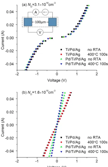
Figure 1. Comparison of I-V curves of Ti/Pd/Ag and Pd/Ti/Pd/Ag
with and without RTA on n-GaAs. The n-GaAs layer doping concentration is: (a) ND = 3.1 x 1018cm 3; (b)
AfD = 1.6 x 1019 cm 3. As sketched by the inset, I-V curves were
measured between pads separated 100 /¿m.
[31] and <j>B ~ 0.85-0.9 eV for Pd/n-GaAs [32]. After RTA no
big changes are observed in either contact since the I-V curves of all samples in figure 1(a) almost overlap. This result was surprising since it was expected that the widely reported reac-tions that occur between Pd and GaAs producing PdGaAs phases [29] would more significantly impact the barrier height. However, similar results have been reported in Pd/n-GaAs contacts made on lightly doped GaAs (AD = 3 X 1016cm 3)
where a reduction of only ^0.02 eV was observed on the barrier height after annealing under similar conditions [33]. So, in essence, our results indicate that the introduction of a Pd layer between n-GaAs and the Ti/Pd/Ag has little influence on the contact resistance when deposited on lightly doped n-GaAs.
On the contrary, the situation on the highly doped sam-ples changes notably as shown in figure 1(b). As illustrated in this figure, all the contacts made on n-GaAs with 7VD = 1.6 x 1019cm 3 have ohmic behavior and, as
com-pared to the I-V curves of Ti/Pd/Ag, the I-V curves of Pd/ Ti/Pd/Ag exhibit lower contact resistance. Hence, the
specific contact resistance and sheet metal resistivity were calculated and listed in table 1. As shown in this table, the specific contact resistance of Pd/Ti/Pd/Ag on highly doped n-GaAs (1.6 x 1019cm 3) is 5.8 x 10 4 O cm2 and, after
RTA, it decreases to 9.7 x 10 5 O cm2. This value is lower
than the Ti/Pd/Ag specific contact resistance after RTA by a factor of 15. In both cases, it seems likely that the high doping in the GaAs thins the barrier to a point where both contacts behave as ohmic. However, the notable difference between them suggests a more efficient tunneling—i.e. a thinner or lower barrier—in the case of Pd/Ti/Pd/Ag contacts. The physical processes behind this improvement could be the ability of Pd to dissolve surface native oxides of GaAs yielding to thinner barriers. Also the possibility of a lower barrier cannot be ruled out since the high doping in the GaAs could enhance somehow the formation of PdGaAs phases during RTA [19, 29].
In regard to the metal sheet resistivity, all the samples of Ti/Pd/Ag and Pd/Ti/Pd/Ag have similar performance. Before RTA, the metal resistivity is ^2.0 x 10 6 O cm, and
after RTA, it increases slightly to ~2.4 x 10 6 O cm. The
small difference may be due to deterioration of Ag con-ductivity caused by limited diffusion from the GaAs to the Ag layer during the RTA. Nevertheless, these values are still nearly one order of magnitude better than the classic metal-lization AuGe/Ni/Au, which shows a sheet resistivity of 1.1 x 10 5 O cm. These results confirm that introducing a Pd
interfacial layer has minimal influence on the performance of the Ti/Pd bilayer that works as an effective barrier to restrict the contamination of Ag by GaAs.
However, although the introduction of the Pd layer decreased considerably the metal-semiconductor specific contact resistance of the contact (by a factor of 15), the final value reached is still far from that of the classic metallization AuGe/Ni/Au with pc = 2.9 x 10 6 O cm2. Therefore, with
the target of obtaining lower specific contact resistances, an interfacial Pd/Ge bilayer was introduced between the n-GaAs layer and the Ti/Pd/Ag metal system. According to the lit-erature, in order to obtain the lowest contact resistance, Ge must be in excess in the Pd/Ge bilayer (i.e. the atomic ratio in the layers must be Pd/Ge < 1, which corresponds to a thickness ratio of Pd/Ge < 2/3) [21, 26, 34]. Accordingly, a Pd/Ge thickness ratio around 1/2 was widely used in these works (45/90, 50/100, 60/130, 75/135 nm) [21, 26, 34] and hence all the Pd/Ge layers in our samples were fabricated with such thickness ratio of 1/2. As shown in table 2, the standard thickness combination chosen in our experiments was 50/100 nm. However, for the samples doped 2.5 x 1018 cm 3 (namely, samples c, d and e in table 2), three
different thickness of Pd/Ge (50/100, 30/60, 15/30 nm) were fabricated to study the impact of total thickness for the bilayer, as will be discussed below.
0.04
0.02
-£ 0.00
CD
-0.02
-0.04
• * a
^ * a
« • a
4 »
a»
a 4»
a * M
a # M
a 4rw • M
# M
<r M
to M
' M
a) 1.3x1018 cm
b)1.3x101 8cm
c) 2.5x1018 cm
d)2.5x101 8cm
e)2.5x101 8cm
f)1.6x101 9cm
g)1.6x101 9cm
Pd/Ge 50/1 OOnm
Pd/Ge 50/1 OOnm
Pd/Ge 50/1 OOnm
Pd/Ge 30/60nm
Pd/Ge 15/30nm
Pd/Ge 50/1 OOnm
AuGe 200nm
-0.6 -0.4 -0.2 0.0 0.2
Voltage (V)
0.4 0.6
Figure 2.I-V curves of Pd/Ge/Ti/Pd/Ag contact resistance as a
function of doping level and Pd/Ge thickness. Pad separation is 100 ¡im in all cases. The details of doping concentration and Ge/Pd thickness from sample (a)-(f) are listed in the figure whilst other details are listed in table 2. The I-V curves of the classic AuGe/Ni/ Au metallization have also been included as (g).
table 2. As figure 2 shows, the I-V curves of all samples exhibit ohmic behavior with three slopes that correspond to the three different doping levels used in the n-GaAs contact layer. As shown in table 2, the specific contact resistances of all these samples are much lower than in the case of a single Pd interfacial layer (table 1). In fact, the best values reached for the specific contact resistance (1.5-1.7 x 10 7 O cm2) are
slightly higher than the best reported for Pd/Ge contacts
[21, 26, 34]. We interpret this fact as an indirect proof of the lack of influence of the upper layers in the contact region and in turn an indirect proof of the Ti/Pd bilayer working suc-cessfully as a diffusion barrier, effectively separating the contact interface region and the sheet conductivity region. This hypothesis has been verified by means of TEM and EDX (see figure 3), and will be discussed later.
As shown in table 2, when the doping level is low (1.3 x 1018cm 3), the specific contact resistance is
8.7 x 10 7 O cm2 after RTA at 300 °C, 20 s. Extending the
RTA time to 60 s does not improve the results, which are in fact a factor of 2 larger. For this reason, we decided to fix our alloying times to 20 s [26, 35]. When the doping level is 2.5 x 1018cm 3, the results are much better: sample d (30/
60 nm) has a specific contact resistance value as low as 1.5 x 10 7 O cm2, whilst sample c (50/100 nm) reaches
vir-tually the same value (1.7 x 10 7 Ocm2). These values are an
order of magnitude lower than those attained with the classic AuGe/Ni/Au (sample g with pc = 2.9 x 10 6 O cm2).
How-ever, for sample e with Pd/Ge thickness of 15/30 nm, the results deteriorate to 1.05 x 10 5 O cm2. This increase of two
orders of magnitude in the specific contact resistance seems to suggest that the Pd/Ge interfacial bilayer is not thick enough in this case (15/30 nm) for the solid phase regrowth process to proceed appropriately. Finally, for the highly doped sample (1.6 x 1019cm 3), the value of the specific contact resistance
obtained (2.5 x 10 6 O cm2) is an order of magnitude higher
than that of samples c or d, albeit still very low and good enough
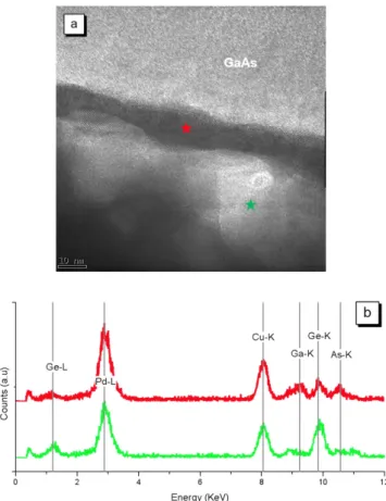
Energy (KeV)
Figure 3. (a) Cross-sectional TEM image of sample c in table 2; (b) EDX spectra taken from the different points marked with a colored star in figure 3(a). The star and the related EDX spectrum share the same color. The peaks corresponding to the main elements detected in EDX—from left to right Ge, S, Pd, Ag and Ti—are labeled in the plot as vertical lines. The leftmost unlabeled peak corresponds to adventitious C contamination.
can be given to this phenomenon. Further investigations are underway to clarify this issue.
Regarding to the contact sheet resistivity, as shown in table 2, all the Pd/Ge/Ti/Pd/Ag samples have a metal resistivity around 1.9 ~ 2.0 x 10 6 O cm, which is almost
the same as Ti/Pd/Ag without RTA and close to the tabu-lated value for pure bulk Ag (1.6 x 10 6 O cm). It should be
also noted that these resistivities are, on average, around 20% lower than those measured in the Ti/Pd/Ag and Pd/Ti/Pd/ Ag systems (see table 1). We link this result to the fact that the Pd/Ge contact demands lower RTA temperatures (300 °C versus 400 °C) and therefore contamination of the top metal layer is less likely to occur.
In order to further analyze the microstructure of Pd/Ge/ Ti/Pd/Ag contacts and understand the mechanism behind the low contact resistance and low metal resistivity obtained, TEM and EDX measurements were carried out. Figure 3(a) shows a cross section TEM image of sample c in table 2. The chemical composition along the metallization has been mea-sured by means of EDX in figure 3(b), where the spectra for the different layers identified in figure 3(a) are gathered. The main elements detected in EDX—from left to right in figure 3(b), Ge, S, Pd, Ag and Ti—are marked in the plot in order to compare the composition throughout the contact. As shown in figures 3(a) and (b), a uniform dark 50 nm layer (marked with a blue star) is clearly visible in the middle of the image. This band can be identified as a Pd layer, according to the corresponding EDX spectrum (blue line in figure 3(b)). The EDX analysis of the layer above (red line figure 3(b)) shows an Ag layer with no signal of Ga or As (Ga and As should appear at energies >9 keV, not shown in the figure to enlarge the relevant portion of the jc-axis). This proves that neither Ga nor As significantly diffuse into the top Ag layer, and thus indicates that the Ti/Pd barrier layer works fine with the moderate RTA process needed for this contact (300 °C and 20 s). The sulfur detected in the Ag layer is related to contamination from the laboratory ambient where the samples were stored (i.e. silver sulfuration). In the green star region of figure 3(a), below the Pd layer, the Ti layer is identified. Some amount of Ag is also detected in this layer illustrating that Ag diffuses into the Ti layer to a certain extent. However, in the next layer (orange star region), only Pd and Ge are measured by the EDX analysis (no significant Ag is detected), sug-gesting that a 50 nm Ti layer is thick enough to stop the Ag diffusion for our RTA conditions. Finally, in the contact region close to the interface (marked with an orange star) both Pd and Ge are detected evidencing a clear intermixing of the Pd and Ge layers.
The interface of Pd/Ge/Ti/Pd/Ag has been measured in more detail by high resolution TEM (HRTEM) and key results are summarized in figure 4(a). Additionally, chemical composition has been analyzed by taking punctual EDX spectra (figure 4(b)). The green spectrum in figure 4(b) (corresponding to the location marked with a green star in figure 4(a)) corroborates the existence of a Pd/Ge layer with a very low Ga and As detection. Between the GaAs and the Pd/ Ge, a 10 nm darker band is observed (marked with the red star in figure 4(a)). Jong-Lam Lee et al [26] reported that this band
Energy (KeV)
Figure 4. (a) Cross-sectional high resolution TEM image of the
contact interface region of sample c in table 2; (b) EDX spectrum taken from the points marked with a red and green star. The star and the related EDX spectrum share the same color. The peaks corresponding to the main elements detected in EDX-from left to right Ge, Pd, Cu, Ga, Ge and As—are labeled in the plot as vertical lines. The leftmost unlabeled peak corresponds to adventitious C contamination. The presence of Cu represents contamination from the sample holder.
was a Ge epitaxial layer resulting from the regrowth of excess amorphous Ge. However, our EDX results show that this layer contains Pd, Ga, Ge and As (red spectrum in figure 4(b)) that can be associated to a Pd4(GaAs, Ge2) intermediate
compound previously reported [36]. The detection of Cu in this spectrum should be neglected since it is attributed to contamination from the sample holder.
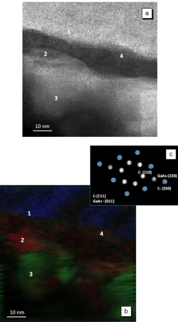
Figure 5(a) shows a higher magnification HRTEM image of the interface. This figure was analyzed with the inverse fast Fourier transform method (FFT) and the different crystal-lographic structures have been identified and isolated. Figure 5(b) represents a false color plot of figure 5(a) that synthesizes this crystallographic information by assigning a different color to a range of nearest-neighbor bond lengths. Different control points, labeled from 1 to 4, have been added in both figures 5(a) and (b) to identify different regions. The blue zone in figure 5(b) (i.e. point 1) corresponds to the zone axis [011] of the GaAs substrate. The green region (i.e. point 3) is formed by interplanar distances of 0.275 nm and 0.224nm that can be associated with the planes (111) and (110) of compound Ge0.4Pd36 whose lattice constant is
Figure 5. (a) Cross-sectional high resolution TEM image of the
contact interface region sample c of table 2; (b) false color plot of figure 5(a), where different lattice parameters are indicated with different colors; (c) diffraction pattern of points 1 and 4 (details in the text).
spectrum present in figure 4(b), where we observed GePd regions just above the dark band layer. Finally, the FFT associated with the red region (i.e. point 4) is included in figure 5(c) with white dots. In this figure, the prefix C- in the labels has been used to denote the planes related to this compound. Additionally, the resultant FFT for the GaAs substrate (blue region in figure 5(b)) has been overlapped in the same figure 5(c) using blue dots, and has been labeled as GaAs-[Oil] zone axis. The analysis of this diffraction pattern suggests that the interfacial layer is a cubic structure oriented in the [111] zone axis with a calculated lattice parameter of around 0.848 nm. As it has been mentioned, this layer is most likely Pd4(GaAs, Ge2) as previously reported, since the EDX
spectra measured at that position revealed the existence of Ge, Pd, As and Ga. It is important to note that the plane (330) of this layer has almost the same value as GaAs (220), i.e.:
d = 0.199 nm. This fact is an evidence of epitaxial growth, as can be observed in the HRTEM of figure 5(b).
In the literature several interpretations exist to explain the good performance of Pd/Ge contacts on GaAs. In short, after the initial formation of intermediate PdGaAs phases, Ge dif-fuses inwards and drives the decomposition of PdGaAs forming GePd [21, 24-26, 36]. At this point, some works claim that the excess Germanium creates an epitaxial layer on the GaAs (i.e. the low specific contact resistance is the result of surface bandgap lowering by Ge) [21, 25]; other works suggest that excess Ge and dissolution of the PdGaAs phases create a newly regrown epitaxial n++GaAs layer (i.e.
Ge + PdGaAs - • n++GaAs + GePd) [24, 36]; and finally
other works simply claim that excess Ge diffuses into the GaAs to form a n+ + superficial layer, which is responsible for
the low specific contact resistance by enhancing the tunneling probability [24, 26].
However, in our HRTEM analysis we did not detect any Ge epitaxial layer at the contact interface. The complete decomposition of the PdGaAs phase was not confirmed either. On the contrary, we found an epitaxial Pd4(GaAs, Ge2)
compound in contact to GaAs. Therefore, our vision of the process is that this intermediate compound changes the metal/semiconductor barrier height, and thus a very low specific contact resistance is obtained due to the enhanced tunneling. It is also likely that a very thin n++GaAs region
exists at the interface since out-diffusion of Ga and As into the Pd4(GaAs, Ge2) will favor the in-diffusion of Ge into the
semiconductor.
Summary and conclusion
Pd/Ti/Pd/Ag and Pd/Ge/Ti/Pd/Ag metallizations on n-GaAs have been studied in the quest for a metal system that can provide (1) low metal/semiconductor specific contact resistance; (2) high metal conductivity; (3) long term stability; (4) good bondability; and (5) low cost (as compared to other systems including Au or Pt). This study has been conducted analyzing the contact performance on n-GaAs of various doping concentrations and comparing the results to Ti/Pd/Ag and Au/Ge/Ni/Au metal systems.
The results show that Pd/Ti/Pd/Ag produced Schottky-like I-V curves when deposited on n-GaAs doped 3 x 1018cm 3, and became ohmic when deposited on
n-GaAs doped 1.6 x 1019 cm 3. In this latter case, the
metal-semiconductor specific contact resistance obtained was of pc ~ 10 4 O cm2, an order of magnitude lower than those
formed using Ti/Pd/Ag (pc ~ 10 3 O cm2). On the other
hand, Pd/Ge/Ti/Pd/Ag contacts achieved a very low pc =
1.5 x 10 7 O cm2 with NB = 2.5 x 10¹⁸Ocm2.
Micro-structure analysis on the contact interface carried out by HRTEM reveals that this low specific contact resistance can be attributed to the formation of a Pd4(GaAs, Ge2) compound
in contact to n++GaAs.
the metal resistivities of both layers (pw ~ 2 x 10~&ilcm) are similar to the values attained with T i / P d / A g and quite close that of pure bulk Ag. These results indicate that the presence of Pd or P d / G e as interfacial layers does not sig-nificantly interfere with the diffusion barrier effect of Ti/Pd, which prevents the contamination of Ag from GaAs diffusion. This was confirmed by the microstructure analysis by TEM and EDX, that measured negligible contamination of Ga and As into the Ag layer and vice versa.
Finally, as compared to the classic A u G e / N i / A u contact layer, P d / G e / T i / P d / A g shows a factor 20 lower specific contact resistance and one order of magnitude lower metal resistivity. As a result of such good electrical properties, plus its cost-effectiveness, it exhibits high potential for applica-tions on electronic devices that need to handle high current densities.
Acknowledgments
Mr Huo Pengyun acknowledges financial support of the China Scholarship Council for his PhD. This work was sup-ported by the Spanish Ministerio de Economía y Competiti-vidad through project with reference TEC2015-66722-R. We also acknowledge Fundación Iberdrola for their financial support within the program 'Ayudas a la Investigación en Energía y Medioambiente'. We also want to thank Mr Brian Li for his proofreading of the manuscript.
References
[1] Brillson L J 1993 Contacts to Semiconductors: Fundamentals
and Technology (Park Ridge, NJ: Noyes) p 1-2 ISBN
9780815513360
[2] Schroder D K and Meier D L 1984 Solar cell contact resistance —a review IEEE Trans. Electron Devices 31 637^-7 [3] Meier D L and Schroder D K 1984 Contact resistance: Its
measurement and relative importance to power loss in a solar cell IEEE Trans. Electron Devices 31 647-53 [4] Burgers A R 1999 How to design optimal metallization
patterns for solar cells Prog. Photovolt. Res. Appl. 7 457-61 [5] Shabana M M, Saleh M B and Solimán M M 1989
Optimization of grid design for solar cells at different illumination levels Sol. Cells 26 177-87
[6] Blank T V and Gol'dberg Y A 2007 Mechanisms of current flow in metal-semiconductor ohmic contacts
Semiconductors 41 1263-92
[7] Rideout V L 1975 A review of the theory and technology for ohmic contacts to group III-V compound semiconductors
Solid-State Electron. 18 541-50
[8] Piotrowska A, Guivarc'h A and Pelous G 1983 Ohmic contacts to III-V compound semiconductors: a review of fabrication techniques Solid-State Electron. 26 179-97
[9] Piotrowska A 1993 Ohmic contacts to GaAs: fundamentals and practice Acta Phys. Pol. A 84 491-504
[10] Baca A G, Ren F, Zolper J C, Briggs R D and Pearton S J 1997 A survey of ohmic contacts to III-V compound
semiconductors Thin Solid Films 308-309 599-606
[11] Braslau N, Gunn J B and Staples J L 1967
Metal-semiconductor contacts for GaAs bulk effect devices
Solid-State Electron. 10 381-3
[12] Kuan T S, Batson P E, Jackson T N, Rupprecht H and Wilkie E L 1983 Electron microscope studies of an alloyed Au/Ni/Au-Ge ohmic contact to GaAs J. Appl. Phys. 54 6952
[13] Shih Y-C, Murakami M, Wilkie E L and Callegari A C 1987 Effects of interfacial microstructure on uniformity and thermal stability of AuNiGe ohmic contact to n-type GaAs
J. Appl. Phys. 62 582
[14] Sai Saravanan G, Mahadeva Bhat K, Dhamodaran S, Pathak A P, Muralidharan R, Vyas H P, Sridhara Rao D V, Balamuralikrishnan R and Muraleedharan K 2015 Evolution of surface morphology of alloyed AuGe/Ni/Au ohmic contacts to GaAs microwave FETs Mater. Sci. Semicond.
Process. 30 62-74
[15] Wang Y, Liu D, Feng G, Ye Z, Gao Z and Wang X 2015 Effect of Pt diffusion barrier layer in Ni/AuGe/Pt/Au on ohmic contact to n-GaAs J. Semicond. 36 036002
[16] Baca A G and Ashby C I 2005 Fabrication of GaAs Devices (London: Institution of Electrical Engineers) p 194 ISBN: 0863413536
[17] Zhou J, Xia G, Li B and Liu W 2003 Structural and electrical properties of Au/Pt/Ti ohmic contacts to degenerated doped n-GaAs Appl. Phys. A 76 939^12
[18] Cotal H, Fetzer C, Boisvert J, Kinsey G, King R, Hebert P, Yoon H and Karam N 2009 III-V multijunction solar cells for concentrating photovoltaics Energy Environ. Sci. 2
174-92
[19] Chong W K, Chor E F, Heng C H and Chua S J 1997 (Pd, Ti, Au)—based ohmic contacts to p- and n-doped
Ino.53Gao.47As Proc. of the IEEE 24th Int. Symp. on Compound Semiconductors 1997. (San Diego, CA, 1998)
pp 1 7 1 ^
[20] Huo P and Rey-Stolle I 2016 Ti/Pd/Ag Contacts to n-Type GaAs for high current density devices J. Electron. Mater. 45 2769-75
[21] Ivey D G, Eicher S, Wingar S and Lester T 1997 Performance of Pd-Ge based ohmic contacts to n-type GaAs J. Mater.
Sci, Mater. Electron. 8 63-8
[22] Hsu C H, Chang H J, Yu H W, Nguyen H Q, Ma J S and Chang E Y 2014 Gold-free Cu-metallized III-V solar cell
IEEE Int. Conf. on Semiconductor Electronics (ICSE2014) (Kuala Lumpur, 2014) pp 336-8
[23] Gutsche C, Lysov A, Regolin I, Brodt A, Liborius L, Frohleiks J, Prost W and Tegude F J 2011 Ohmic contacts to n-GaAs nanowires J. Appl. Phys. 110 014305
[24] Lai J T and Lee J Y-M 1994 Redistribution of constituent elements in Pd/Ge contacts to n-type GaAs using rapid thermal annealing J. Appl. Phys. 76 1686
[25] Lim J-W, Mun J-K, An S-J, Nam S, Kwak M-H, Kim H and Lee J-J 2000 PdGe-based ohmic contact on n-GaAs with highly and poorly doped layers Japan. J. Appl. Phys. 39
2546-9
[26] Lee J-L, Kim Y-T, Oh J-W and Lee B-T 2001 AlGaAs/ InGaAs pseudomorphic high electron mobility transistor using Pd/Ge ohmic contact Japan. J. Appl. Phys. 40
1188-93
[27] Jones K A, Cole M W, Han W Y, Eckart D W, Hilton K P, Crouch M A and Hughes B H 1997 Comparison of PdGeTiPt and NiGeAu ohmic contacts to n-GaAs and PdGeTiPt and TiPd contacts to p[sup +]-GaAs J. Appl.
Phys. 82 1723
[28] Huang W C, Lei T F and Lee C L 1994 Pd-Ge contact to n-GaAs with the TiW diffusion barrier J. Electron. Mater. 23 397^101
[30] Van der Pauw L J 1958 A method of measuring specific resistivity and Hall effect of discs of arbitrary shape Philips
Res. Rep. 13 1-9
[31] Goksu T, Yildinm N, Korkut H, Ózdemir A F, Turut A and Kokce A 2010 Barrier height temperature coefficient in ideal Ti/n-GaAs Schottky contacts Microelectron. Eng. 87 1 7 8 1 ^ [32] Heng-Yong N and Yasuo N 1991 Pd-on-GaAs Schottky
contact: its barrier height and response to hydrogen Japan. J.
Appl. Phys. 30 906
[33] Eftekhari G 1995 Electrical studies of rapidly annealed Ni and Pd/n-GaAs Schottky diodes Japan. J. Appl. Phys. 34 2247-51
[34] Machác P and Penna V 2003 Role of reactive metals in Ge/ Pd/GaAs contact structures Microelectron. Eng. 65 335^43 [35] Kim I-H 2003 Comparison of Pd/Ge/Pd/Ti/Au and Pd/Ge/
Ti/Pt ohmic contacts to n-type InGaAs Mater. Jjett. 57 4033-9
[36] Brillson L J 1993 Contacts to Semiconductors: Fundamentals
and Technology (Park Ridge, NJ: Noyes) p 37 ISBN
9780815513360